SoC Encounter for Designers II - Integrated Systems Laboratory
SoC Encounter for Designers II - Integrated Systems Laboratory
SoC Encounter for Designers II - Integrated Systems Laboratory

You also want an ePaper? Increase the reach of your titles
YUMPU automatically turns print PDFs into web optimized ePapers that Google loves.
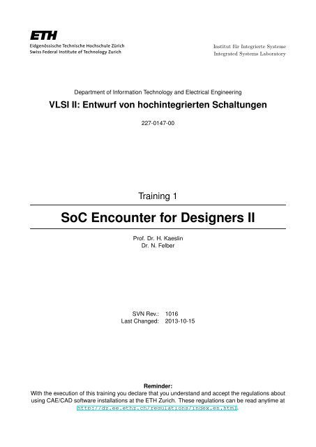
Institut für Integrierte Systeme<strong>Integrated</strong> <strong>Systems</strong> <strong>Laboratory</strong>Department of In<strong>for</strong>mation Technology and Electrical EngineeringVLSI <strong>II</strong>: Entwurf von hochintegrierten Schaltungen227-0147-00Training 1<strong>SoC</strong> <strong>Encounter</strong> <strong>for</strong> <strong>Designers</strong> <strong>II</strong>Prof. Dr. H. KaeslinDr. N. FelberSVN Rev.: 1016Last Changed: 2013-10-15Reminder:With the execution of this training you declare that you understand and accept the regulations aboutusing CAE/CAD software installations at the ETH Zurich. These regulations can be read anytime athttp://dz.ee.ethz.ch/regulations/index.en.html.
1 OverviewUnlike other exercises in the VLSI lectures, the back-end design flow requires you to learn how touse a commercial Electronic Design Automation (EDA) tool, in our case CADENCE SOC ENCOUNTERfrom Cadence Design <strong>Systems</strong>. These exercises are there<strong>for</strong>e called ’Trainings’ and will teach youthe basics of CADENCE SOC ENCOUNTER so that you can use it <strong>for</strong> your semester projects.There will be three trainings:• Training 1Floorplanning, placement, clock tree synthesis, optimization, routing and timing analysis withCADENCE SOC ENCOUNTER .• Training 2Determining power consumption, IR drop analysis.• Training 3Tape-out preparation, per<strong>for</strong>ming Design Rule Check (DRC) and Layout Versus Schematic(LVS) on your final database.Students who plan to work on an ASIC semester project should make sure to visit all three trainings.1.1 About the StyleWe will try to use a number of different styles to identify different types of actions. These are summarizedbelow:Student Task: Parts of the text that have a gray background, like the current paragraph, indicatesteps required to complete the exercise.Actions that require you to select a specific menu fill be shown like the following:menu→sub-menu→sub-sub-menuWhenever there is an option or a tab that can be found in the current view/menu we will use a BUTTONto indicate such an option.Throughout the exercise you will be asked to enter certain commands using the commandline 1 . Thefollowing is an example of the linux command line.sh >command to be entered on the linux command lineWhereas some of the commands will be entered on the command line of the CADENCE SOC EN-COUNTER tool such as:enc >this command is an encounter command1There are many reasons <strong>for</strong> using a commandline. Some functionality can not not be accessed through GUI commands,and in some cases, using the commandline will be much faster. Most importantly, things you enter on the commandlinecan be converted into a script and executed repeatedly2
2 IntroductionIn this training we will start with a structural Verilog design netlist (from synthesis) and create step bystep a physical layout that can be manufactured. To keep runtimes reasonably low, we will use anexample design with a (slightly) lower complexity than most student design projects.2.1 Example DesignThe example design is based on the FIR filter that we have been using in the past exercises. The filterhas been changed to include several pipelined filter stages as shown in the block diagram below 2 .ResetxRBIDataInxDIDataInReqxSIDataInAckxSORamWDxDRamAddrxDSY180_2048X16X1CM8 r256x72tb300xoRamRDxDRamTestxTILUT16LUT16LUT16LUT16LUT16ScanEnxTI16321632163216321632DataOutAckxSI48484848484848484848DataOutReqxSO’0’484848484848484848484848484848DataOutxDOClkxCIfilter_stage1filter_stage2filter_stage3filter_stage4filter_stage8filterfiter_topfilter_chipEach filter stage contains a large multiplier, a look-up table and an accumulator. Note that the input ofthe first stage is tied to constants and there<strong>for</strong>e greatly simplified. The following is a short descriptionof all pins of the circuit:2The filter is basically useless and has only been engineered as an example circuit suitable <strong>for</strong> the exercise.3
Pin DescriptionsName Bits Dir DescriptionClkxCI 1 In Clock inputResetxRBI 1 In Reset input, active low signal, 0: ResetScanEnxTI 1 In Scan Enable <strong>for</strong> testing, 1: ScanRamTestxTI 1 In Ram bypass control, 1: Test (RAM bypassed)DataInxDI 16 In 16-bit data inputDataInReqxSI 1 In Request signal <strong>for</strong> data inputDataInAckxSO 1 Out Acknowledge signal <strong>for</strong> data inputDataOutxDO 16 Out 16-bit data outputDataOutReqxSO 1 Out Request signal <strong>for</strong> data outputDataOutAckxSI 1 In Acknowledge signal <strong>for</strong> data output3 Getting StartedYou will need a terminal program to type in commands throughout this exercise. In the computersin the ETZ D61.2 you can get a terminal by accessing the menu on the top left corner and selectingApplications→Accessories→Terminal.Student Task 1:• Change to your home directory and install the training files with the script provided:sh >sh >cd ˜/home/vlsi2/t1/install_t1• Change to the design directorysh >cd training_1The copied files and folders are arranged in a certain structure which is described in the next section.3.1 Directory StructureThe following figure shows the directory structure <strong>for</strong> a design directory that was created by thecockpit tool developed by the Design Zentrum (DZ) of ETH Zurich.4
design.cockpitrccalibredocsConfiguration <strong>for</strong> the cockpitFinal layout, DRC and LVSLinks to documentsencounteroutsavescriptssrctechFinal output files: netlist, layout, timing (Verilog,GDS<strong>II</strong>, SDF)Save files <strong>for</strong> <strong>Encounter</strong> (<strong>Encounter</strong> native <strong>for</strong>mat)Example scripts, run scripts (TCL)Input source files: netlist, constraints, io placementsample Sample input filesLinks to technology files, etc.lef Links to absracts and technologylib Links to timing librariesmodelsimsimvectorssourcecodesynopsystetramaxSimulation toolStimuli and expected responsesVHDL sourcecodeSynthesis environmentTest vector generation, test coverageIn this structure, there are five subdirectories <strong>for</strong> CADENCE SOC ENCOUNTER . It is strongly recommendedto use them in the following way:out Place all final data to be exported from CADENCE SOC ENCOUNTER in this directory. Thisincludes the final netlist (the initial netlist gets modified by clock tree insertion, optimization etc.),layout and delay files that will be used <strong>for</strong> postlayout simulation and/or physical verification andchip finishing. A sample script that generates all these files is provided (scripts/exportall.tcl).save Put all CADENCE SOC ENCOUNTER<strong>for</strong>mat, in this directory.save files, i.e. files in native CADENCE SOC ENCOUNTERscripts Contains TCL scripts. By default several example scripts <strong>for</strong> common tasks are provided. Itis highly recommended to develop a run script that contains all the commands used <strong>for</strong> yourdesign.src All user input files should be placed here. These include the initial Verilog netlist, the I/O placementfile, timing constraints file and clock tree definition file (all will be explained later in section3.2).tech Holds links to technology specific files. Cockpit manages this directory automatically.3.2 Input FilesThe input files required <strong>for</strong> back-end design with CADENCE SOC ENCOUNTERtwo categories:can be divided into• Design files that describe (or are closely related with) the circuit, first of all the Verilog netlist ofour synthesized design.• Technology files that describe the technology itself as well as libraries of standard buildingblocks implemented in this technology.5
Let’s start with the first category.3.2.1 Verilog NetlistThe Verilog netlist we obtain from synthesis contains standard cells, functional I/O pads and theirinterconnection in<strong>for</strong>mation. While the functionality including scan circuitry is already complete, somespecial cells are still missing:• Supply pads to provide power and ground to the core (pads ’VCCKD’ and ’GNDKD’) and to thepadframe (pads ’VCC3IOD’ and ’GNDIOD’).• Corner pads that need to be placed in the corners of the padframe to complete the power linesrunning inside the padframe (pad CORNERD).Due to the arrangement we have with our ASIC manufacturer, student designs are strictly limited insize. As a consequence at most 56 pads (not including the 4 corner pads) can be placed in thepadframe. Furthermore, to ease chip testing on the ASIC tester two predefined power schemes havebeen established:1. 40 signal pads, 16 supply padsTake a look at the following web page <strong>for</strong> an illustration of the power schemes and to obtain furtherin<strong>for</strong>mation on constraints <strong>for</strong> the semester design projects.http://www.eda.ee.ethz.ch/index.php/UmcL180#Mini.40sicWith all this in<strong>for</strong>mation we are now ready to add the missing corner and supply pads to our Verilognetlist.A typical Verilog netlist that you will obtain from SYNOPSYS DESIGN COMPILER will contain manylevels of hierarchy. Each level of hierarchy is enclosed between themodule name ( pin names separated by comma )...endmodulestatements, where ’name’ refers to the name of the module (module is the Verilog equivalent of anentity in VHDL). In our case we need to add the pads to the top-level module which contains the restof the I/O pads. The top-level design is almost always the last module definition in a Verilog file 3 .Student Task 2:• Copy the Verilog netlist to encounter/src/ in order to have a clean copy of the initial netlisteven if synthesis is rerun.sh > cd encounter/src/sh > cp -p ../../synopsys/netlists/filter_chip.v \filter_chip.v.initialThe file specialpads.v contains four corner pads and 8 supply pads corresponding to thepower scheme 1. As our design uses power scheme 1, no changes are required to this3The content of the module needs to be defined be<strong>for</strong>e it can be instantiated by a different module. Consequently thetop-level module is the last to be defined, however not all Verilog files need to be hierarchical, a design can also bespread between multiple files6
file. For power scheme 2, we would have to comment out the eight additional supply pads(comments in Verilog start with //).What remains to do is to add the contents of specialpads.v at the right point, i.e. where theother pads are, to the initial netlist.• Using a text editor a , open filter chip.v.initial and find the definition of the top-level module’chip’ by searching <strong>for</strong>:module chipBelow this declaration you should see lines that instantiate the pads. Insert the contents ofspecialpads.v at this point. As long as you are in the module body, it does not matter whereexactly you insert them.• Save the file as filter chip.v and exit the text editor.aThere are many text editors you can use. There are terminal based editors (vi, vim, nvi, joe, jed, pico, nano etc.),editors that are mainly terminal based but have a simple GUI (emacs, xemacs, gvim etc), and GUI based editors(mousepad, gedit, nedit, kate etc). Out of these emacs, vi (and derivatives), and nedit are the most advancededitors.Remark: In the future you can use a small Perl script to add the specialpads to the initial netlist, i.e.sh > ./insert_specialpads ../../synopsys/netlists/filter_chip.v \./specialpads.v > filter_chip.vinserts the contents of specialpads.v into the last module defined in ../synopsys/netlists/filter chip.vand write the modified netlist to filter chip.v.3.2.2 I/O FileAfter the last step our Verilog netlist contains all pads. However there is no in<strong>for</strong>mation that actuallytells the tool where each pad should be placed. The pad placement is very important as it directlydetermines the PCB layout 4 . In our case, we want all designs to share a common power and groundpad locations so that a single test board can be used on our ASIC tester. For practical reasons wehave decided to use a 56-pin package <strong>for</strong> all designs. So even though the chip has only 48 physicalpins, it will be placed in a package that contains 56 pins 5 . Depending on the power configuration,a different bonding scheme will be used. These two configurations can be seen on the followingwebpage:http://www.eda.ee.ethz.ch/index.php/UmcL180#Mini.40sicThe cockpit will copy sample I/O files automatically to the src/sample directory 6 . All lines startingwith ‘#‘ are comments. The file consists of two main sections: globals and iopad.(globals[global definitions]456A good pinout could simplify the routing on the PCB, allow you to use fewer layers and result in less parasitics8 pins will be left unconnectedFor this technology there will be four files. There will be two template files chip.io−template and chip−ep.io−template<strong>for</strong> the normal and extended power configuration respectively. These files have all the required power connections inplace, and the data sections are commented out. There are also two example files that have fictional I/O placementwhere all pins are defined.7
)(iopad(topleft[pads that are on the top left])(left[pads that are on the left side]))[definitions <strong>for</strong> other sides]For us the relevant part is the iopad section. This part contains eight subsections that define thenames of the pad instances, and their locations in the four sides and four corners. We do not haveto touch the corner specifications 7 as they will be the same <strong>for</strong> all designs. We have to distribute thepads among the four sides of the chip top, right, bottom, left. If you look at the sample file youwill see that <strong>for</strong> each pad there is a single line entry in the following <strong>for</strong>m(inst name="NAME_OF_PAD"offset=OFFSET_VALUE ) # pin no: PIN_NUMBERThe last part following # is a comment, it is there just <strong>for</strong> your in<strong>for</strong>mation. Regardless of the powerscheme you are using, we will use the same 56 pin package as illustrated in the webpage above.The PIN_NUMBER is just a reminder to show which particular location is being defined. The locationis specified using the OFFSET_VALUE. CADENCE SOC ENCOUNTER uses a coordinate system thatbases the coordinate (0,0) on the bottomleft corner as shown in the figure below:toplefttoptopright123leftrightSideOffset0,0bottomleftbottombottomrightOn the left and right side the pads will be ordered from bottom-to-top, and on the top andbottom side the pads will be ordered from left-to-right. This ordering can be quite confusing, asit is neither clockwise, nor counterclockwise. There<strong>for</strong>e the a<strong>for</strong>ementioned comments showing theactual pin numbers will be very useful.7topleft, topright, bottomleft, bottomright8
The OFFSET_VALUEs given in the template represent fixed locations <strong>for</strong> the given pad. It is veryimportant that you do not change these values, as the chip-finishing part will rely on the pads beinglocated exactly at these locations.You can assign your pads by writing the name of each pad into the corresponding NAME_OF_PAD.The name of the pad will be the name of the instance in the Verilog file. For example assume that youare using standard power scheme and your clock signal is assigned to a pad named pad_clock. Inyour Verilog file you would have the following entry <strong>for</strong> this pad:XMD ClkxCI_PAD ( .I(ClkxCI) [other pin definitions] )If you now want to place this pad on pin number 54 of your package, you will find the subsection topin the I/O file and edit the line <strong>for</strong> pin 54:...(iopad...(top...(inst name="ClkxCI_PAD" offset= 864.28 ) # pin no: 48...)...)Be careful, do not modify the offset value while you are editing the I/O file. Since we use a fixedbonding scheme <strong>for</strong> the power and ground pins, all we need to do is extract the instance names <strong>for</strong>all our signal pads and place them by inserting within the appropriate inst name="" statement correspondingthe OFFSET_VALUE which corresponds to the desired location. It is also recommendedto put the clock pin (if possible) to pin number 48. All new test boards will make sure that the pin 48has the best signal quality.Preparing the I/O file from scratch can be a lengthy and tedious task. To avoid unnecessary workduring this exercise we will start with an almost complete I/O file, but be<strong>for</strong>e doing so we will describethe full procedure recommended when starting from scratch:1. Start CADENCE SOC ENCOUNTER and proceed to design import 8 by selecting Design→\Import Design. In this <strong>for</strong>m make sure that the IO ASSIGNMENT FILE is empty.2. If everything works well, the design will be loaded. Now we can write out a template file that willcontain all the names of the pads. Use Design→Save →I/O File ... to save an I/O filesrc/chip−sequence.io. You can select the SEQUENCE checkbox, however it is not imperative.What we need is only the names of the pads.3. Copy the template I/O file src/sample/chip.io−template to src/chip.io. As noted earlier, this fileincludes all offset= statements, and all statements <strong>for</strong> corner and supply pads.4. Using a text editor open the files src/chip.io and src/chip−sequence.io. You need to move thePAD_NAMEs from the file src/chip−sequence.io to the correct positions in the file src/chip.io.5. All entries <strong>for</strong> data pins in the template file are by default commented out using ‘#‘ character.Do not <strong>for</strong>get to remove the comment character <strong>for</strong> the pads you are using.8Importing the design will be covered in detail in Chapter 4.9
Student Task 3:• Now, <strong>for</strong> this exercise you can start with the almost complete I/O file src/chip.io−incomplete\instead of the template file. This file has all the pads placed properly with the exception ofthe 16 pads of the input bus DataInxDI which are still missing.Furthermore the file src/filter chip.sequence.io mentioned above has already been generated<strong>for</strong> you.The desired I/O assignment is depicted in the figure below and can also be found in the filesrc/filter chip.io.ps a .• Create the complete I/O file and save it as src/filter chip.io.aPostscript viewers were very common in the earlier days, you can use gv, kghostview, or evince to view this fileYou can use the utility src/io2ps.pl to generate a postscript file from your I/O file. This utility will alsoverify if you have used the correct offset locations in you I/O file, and will report errors. For bestresults, you should also provide the Verilog netlist file, which will enable the script to make even morechecks.sh >./io2ps.pl filter_chip.io > filter_chip.pin_diagram.psThe src/io2ps.pl utility uses a configuration file with the extension .pads. Per default the file src/io2ps\.pads will be used. If you are planning to use the extended power scheme, you will have to add theconfiguration file src/io2ps−ep.pads to the command as well.pad_vcc_p11565554535251504948474645444342pad_gnd_p3DataInxDI_PAD_9241DataOutxDO_PAD_11DataInxDI_PAD_8340DataOutxDO_PAD_10DataInxDI_PAD_7439DataOutxDO_PAD_9DataInxDI_PAD_6538DataOutxDO_PAD_8DataInxDI_PAD_5637DataOutxDO_PAD_7pad_gnd_c1736pad_vcc_c3pad_vcc_c1835pad_gnd_c3DataInxDI_PAD_4934DataOutxDO_PAD_6DataInxDI_PAD_31033DataOutxDO_PAD_5DataInxDI_PAD_21132DataOutxDO_PAD_4DataInxDI_PAD_11231DataOutxDO_PAD_3DataInxDI_PAD_01330DataOutxDO_PAD_2pad_gnd_p114151617181920212223242526272829pad_vcc_p3pad_vcc_p2DataInxDI_PAD_10DataInxDI_PAD_11DataInxDI_PAD_12DataInxDI_PAD_13DataInxDI_PAD_14pad_gnd_c2pad_vcc_c2DataInxDI_PAD_15DataOutAckxSI_PADDataOutReqxSO_PADDataOutxDO_PAD_0DataOutxDO_PAD_1pad_gnd_p2pad_gnd_p4DataOutxDO_PAD_12DataOutxDO_PAD_13DataOutxDO_PAD_14DataOutxDO_PAD_15ResetxRBI_PADpad_vcc_c4pad_gnd_c4ClkxCI_PADScanEnxTI_PADRamTestxTI_PADDataInAckxSO_PADDataInReqxSI_PADpad_vcc_p410
3.2.3 Timing ConstraintsJust as <strong>for</strong> synthesis, we need to specify timing constraints <strong>for</strong> the backend design with CADENCESOC ENCOUNTER .With decreasing process geometries the impact of placement and routing on timing, power, etc. issteadily increasing. There<strong>for</strong>e, timing analysis and optimization have become very important in orderto arrive at a layout that (still) satisfies all requirements.As CADENCE SOC ENCOUNTER supports most of the more common SYNOPSYS DESIGN COMPILERcommands/constraints it should be rather straight <strong>for</strong>ward to create an appropriate timing constraintsfile based on the constraints used <strong>for</strong> synthesis.Student Task 4:• There is an example constraint file src/sample/chip.sdc−sample that contains the mostcommonly used commands along with many useful and important comments.Copy this file to src/chip.sdc and modify it so that the following constraints get set (andnothing else!):– Define a 125 MHz clock– Specify 3.5 ns input delay <strong>for</strong> all inputs– Specify 5.0 ns output delay <strong>for</strong> all outputs– Specify an input transition time of 0.8 ns at all inputs– Specify a 15 pF output load <strong>for</strong> all outputs3.2.4 Technology FilesThe tech directory and the two subdirectories contain technology files that describe the technologyitself as well as libraries of standard building blocks implemented in this technology, i.e. standardcells, pads, RAM/ROM.• Technology files (UMCL180)lef/header6 V55.lef Base technology description, defines metal layers, vias, spacing rules,routingumcL180.capTbl Table used to extract parasitic capacitances and resistances <strong>for</strong> signal andpower wires.streamout.map Layer mapping table used when exporting the final layout in GDS<strong>II</strong> <strong>for</strong>mat.• Library files (standard cells, pads, macro-cells)lef/*.lef Physical description, shape and allowed orientation of cells, layer and shape of pins,blockages, antenna in<strong>for</strong>mation, ...lib/*.lib Functional description, timing and power in<strong>for</strong>mation, maximum load/fanout or transitiontimeallowed, ...11
3.2.5 Macro-cellsThe macro-cells <strong>for</strong> the umcL180 process are created using dedicated memory compilers. The specificmemory compiler we have access to is able to create five different types of macro-cells withvarious capacities:• SU180 : single-port static RAM• SJ180 : dual-port 9 static RAM• SY180 : single-port register-file 10• SZ180 : two-port 11 register-file• SP180 : via programmable ROMThe following parameters are used <strong>for</strong> the macro-cells:• wordsNumber of words in the memory• sub-word sizeNumber of bits within a sub-word of the memory. The sub-word is the smallest unit used <strong>for</strong>data access in the macro-cell 12 .• number of sub-words per data wordThis parameter allows creating multiple sub-words. Each sub-word can be written to separately.For example, A 32-bit RAM can be configured as having a single 32-bit sub-word, or two 16-bitsub-words, four 8-bit sub-words and so on.• column or block multiplexerThis parameter affects the geometry of the macro-block. This can have significant influenceon the per<strong>for</strong>mance of the macro-block. There is no general rule to determine this parameter.Once the memory requirements are known, all possible geometries will be considered and themost suitable one will be determined.There are several available macro cells, their datasheets can be found under:/usr/pack/designkits-1.0-ma/umc_L180/faraday/gen/memaker/200901.1.1/datasheet.dzIf none of the available macro-cells suit your needs more can be easily generated on demand. Pleasecontact the Microelectronics Design Center <strong>for</strong> this purpose.Our example design uses a single-port RAM named SY180_2048X16X1CM8. This RAM has 2048words of 16-bits each (single sub-word) and a block multiplexer of 8. All necessary preparations towork with this macro-cell have already been done, so you do not need to do anything additional <strong>for</strong>this exercise.9dual-port memories have two completely independent access ports. At the same time two separate memory addressescan be accessed <strong>for</strong> both read and write.10 Although the name suggests that the memory is made out of individual registers, it is very similar in design to SRAM.11 In two-port memories, the read and write ports are separate, so you can simultaneously read and write. There aretiming constraints <strong>for</strong> reads and writes to the same address, please refer to the memory compiler manual <strong>for</strong> details.12 In many places this sub-word is referred to as ’byte’. This might be slightly confusing, since a byte is commonlyaccepted to be an in<strong>for</strong>mation unit consisting of 8-bits.12
4 Importing the DesignStudent Task 5:• Start CADENCE SOC ENCOUNTER a either from your design directory by using cockpitsh >sh >sh >cd ˜/training_1icdesign umcL180 &• or from the encounter directory by issuing the commandcd ˜/training_1/encountercds_soc81 encounteraThis exercise uses version 8.1 of the Cadence <strong>SoC</strong> <strong>Encounter</strong> . There are newer versions of these software,however the main principles have not changed much so we will continue to use this version <strong>for</strong> this exercise,newer versions have slightly changed GUI elements, and improved capabilities <strong>for</strong> some functions.We will now import our design.CADENCE SOC ENCOUNTER uses a large configuration file that defines the design and technologyfiles to be loaded as well as some global settings to be applied.Cockpit does automatically generate an appropriate sample configuration file src/sample/chip.confthat should be used to start with.Student Task 6:• Copy the sample file into the src directory.sh >cp src/sample/chip.conf src/filter_chip.conf• Select Design→Import Design ... to open the design import <strong>for</strong>m. This <strong>for</strong>m containsfields <strong>for</strong> all configuration options. At the bottom of this window, there are buttonsto load and save the configuration from/to a file. Use the LOAD ... button to load theconfiguration file we have just copied to the src directory.• On the BASIC tab make sure that VERILOG NETLIST:, TIMING CONSTRAINT FILE: and IOASSIGNMENT FILE: match your design. COMMON TIMING LIBRARIES: and LEF FILES:should already be correct.• On the ADVANCED tab the only setting you might want to adapt <strong>for</strong> your design is theDEFAULT DELAY PIN LIMIT: in the category DELAY CALCULATION. We will explain this later.• Once you are happy with the configuration don’t <strong>for</strong>get to save your changes to the configurationfile.• Click OK to import your design. Monitor the messages on the console <strong>for</strong> errors a .Pay attention to the messages where the timing constraint files is loaded (“Reading timingconstraint file”) to see if everything was accepted! If there are errors, you need to fix them!aYou can ignore warnings (SOCLF-58), (SOCLF-200), (TECHLIB-436), (SOCSYC-2), (EMS-27)13
We are now in the floorplan view of CADENCE SOC ENCOUNTER which displays an empty floorplanwith only the pads placed. All top level module(s) of the netlist are shown as a pink/purple square tothe left and all macro-cells to the right. Note that all standard cells are inside the module(s).5 FloorplanningNow we will have to decide how cells and macro-cells will be placed on our chip. This process iscalled floorplanning. For a standard design, our main concern would be to find a floorplan that willresult in the smallest possible area, while fulfilling all per<strong>for</strong>mance and reliability requirements. Thisis purely driven by economical reasons, since chip costs are mainly determined by the area. In somecases there are additional geometrical constraints. The manufacturing company may impose certain14
limits to the aspect ratio of the final layout 13 , or even dictate the maximum height or width of thelayout.Back-end design is not only used <strong>for</strong> complete chips. Macro-cells that will be part of a larger systemon-chipdesign can also be designed in this way. In such cases there might be even more restrictions.For example, certain metal layers might be reserved <strong>for</strong> the system level.So the question is, “How small can my layout be so that I am still able to fulfill all specifications?”. Asa lower bound, you will need enough area to place all your I/O pads and standard cells. Ideally, interms of area (and assuming your design is not pad limited, see exercise 2), you will want to placestandard cells without leaving extra space in between, completely filling out the core area. This ishardly ever possible because:• The number of interconnections that can pass through a certain area is limited by the numberof metal layers available 14 , wire width and minimum spacing requirements. Depending on theinterconnection overhead, the area above the cells 15 may not be sufficient <strong>for</strong> routing.• Timing is greatly affected by the placement of your cells. Placing them next to each other withno space in between not leave the tool any flexibility in placing cells. This in turn reduces theoptimization options of the tool, like the ability to cluster cells that are closely interconnected.• All designs require power routing <strong>for</strong> operation. Some wires of the power connection limit wherethe cells can be placed, or restrict signal routing which in turn increases the area requirement.• The majority of designs require a clock tree to function. This clock tree is added during the backenddesign. This requires additional area <strong>for</strong> the buffers used in the clock tree. Furthermore,the clock tree synthesis algorithm can produce better results if it has more freedom to place itsbuffers.• Macro-cells, like the RAM in our example, usually require some extra space along the edges sothat they can properly be connected to power and signal lines.• Designs that have a high switching activity require a lot of current <strong>for</strong> a short time which iscalled a surge. The power distribution network may need additional decoupling capacitors tostore some charge that can provide some of the current of the standard cells during such asurge. Additional space <strong>for</strong> these decoupling cells may be required during placement.As a consequence, the standard cell rows (which <strong>for</strong>m the core area) can not be filled completelywith standard cells, in other words there needs to remain some free space in between cells.Utilization indicates to what amount the standard cell rows are filled. 100% utilization is the upperbound where all cells are abutted and there is no extra space, while a utilization of 50% means thathalf of the core area is empty.Usually, it is not possible to predict whether or not it is possible to fulfill all requirements with a certainutilization 16 . You will have to try and find out. This is the main reason why back-end design is aniterative process 17 .13 Especially in MPW runs, a lot of silicon area is wasted if all designs have wildly different dimensions.14 For our technology there are 6 metal layers.15 Cells in our technology use mostly the lowest metal layer Metal-1 and very rarely the Metal-2 <strong>for</strong> internal connections,all other layers are free <strong>for</strong> routing.16 Both placement and routing are separately NP complete problems, without completing the routing and placementyou will not know if it is possible to fulfill the requirements.17 Obviously, technology plays an important role, and it is possible to give certain guidelines <strong>for</strong> a technology. However,backend design is always highly dependent on the design itself. You will usually see in a few iterations what is possibleand what is not.15
5.1 Semester ProjectsThe MPW provider used <strong>for</strong> the semester projects offers modules caled Mini Asic (mini@sic) with asize of 1519.62 µm × 1519.62 µm. There<strong>for</strong>e, the chip size <strong>for</strong> the semester project ASICs is fixed.Please refer to the following web page to learn the details.http://www.eda.ee.ethz.ch/index.php/UmcL180#Mini.40sicAs a consequence, we only have to make sure that our design fits on this area, and there is no needto find the smallest possible layout. We may however need to constrain the core area to make itsmaller if the utilization is too low, since a spread out design has longer interconnections that mayadversely affect timing.5.2 Sketching a FloorplanBe<strong>for</strong>e we go on with CADENCE SOC ENCOUNTER we need to make some planning and understandsome key concepts. The figure on the following page is an example floorplan (not an ideal one) thatshows the important concepts.In CADENCE SOC ENCOUNTER die area corresponds to the total silicon area available to place pads(excluding bonding area <strong>for</strong> this technology) and core cells. For the semester projects this is strictlylimited to 1519.62 µm × 1519.62 µm. All pads (I/O, power and corner) are placed in what is knownas the padframe. The remaining area can be used <strong>for</strong> the core of the chip. For semester projectsthe theoretical maximum <strong>for</strong> core area is 1239.38 µm × 1239.38 µm = 1.54 mm 2 .As can be seen from the figure, the core area is surrounded by a core power ring. In its simplest<strong>for</strong>m this consists of two (one <strong>for</strong> VCC, one <strong>for</strong> GND) wide 18 metal lines that evenly distribute the powerall around the chip. In order to leave room <strong>for</strong> the power ring, we need to leave a certain I/O to corespacing.The standard cells are designed in such a way that, when placed next to each other their VCC andGND pins can be connected with a horizontal power line. These horizontal lines are then extendedto the core power ring. These power connections are relatively narrow (0.76 µm in the technologythat we use) and run over the entire width of the core area. This could be a problem <strong>for</strong> designs thatconsume much power, since the cells towards the middle would not have a good power connection 19 .To improve this, vertical power stripes that connect to the horizontal power lines can be added,thereby <strong>for</strong>ming sort of a mesh.The core area is filled with standard cell rows on which later all standard cells will be placed. In thesame area we will usually also need to make room <strong>for</strong> our macro-cells. Most macro-cells need somefree space around themselves. This free space is required to make signal connections, add a blockpower ring around the macro-cell or simply to prevent standard cells from being placed too close tothe macro-cell. We will define a block halo to specify this free space.18 The width of the metal line depends on the amount of current drawn from the line, you will be able to judge thisbetter after exercise 3 which is dedicated to estimating the power consumption. We will mostly use a width of 20 µm,since this is the widest metal that can be manufactured without slotting (wider metal lines require slots/holes whichbreak up the metal shape).19 The problem is that if much current is drawn, there will be a significant IR drop along the power lines. The cellsin the middle will be supplied with a lower VCC than the ones on the sides. This could dramatically effect theper<strong>for</strong>mance of the system.16
When placing a macro-cell, you should also take into account where the power and signal pins of theblock are located and what metal layer they are on. Often signal connections are only on two edgesand you want them to face the core and not the I/O pads.Now, when we consider all the above, the core area that remains free to place core cells on is muchsmaller than the 1.54 mm 2 that we started with. Our example design has a total cell area (includingRAM) of 0.82 mm 2 and should there<strong>for</strong>e com<strong>for</strong>tably fit into the designated area.1519.62 µmVDDGNDStandard Cell Power ConnectionsPower StripeStandard Cell RowBlock Power RingStandard CellsMacro Cell(RAM)1239.38 µmI/O and Corner PadsPlaced on the PadframeBlock HaloBlock Power ConnectionCore Power RingPower Pad ConnectionsI/O to CoreSpacing5.3 Initialize FloorplanWe are now ready to proceed with CADENCE SOC ENCOUNTER .Student Task 7:• From the menu select Floorplan→Specify Floorplan.... A large window will open.• Select the DIE SIZE BY: WIDTH AND HEIGHT option and make sure that both values are1519.62.• Now we need to specify the I/O to core spacing by filling in the four values under the COREMARGINS BY: entry. There must be sufficient room <strong>for</strong> the power ring around the core area.17
Larger values will reduce the area available to place the core cells thereby increasing coreutilization.As noted earlier, some iterations are usually required to find optimal values <strong>for</strong> a particulardesign.• In this exercise we will assume that we will use one VCC and one GND line of maximumwidth 20 µm. We need some extra space between the lines and, <strong>for</strong> the moment, we canstart with a distance of 50 µm <strong>for</strong> all sides and click on OK.The floorplan should now look like shown in the screen-shot below. Note that the pads are all placedat their proper locations as the I/O file used during design import specifies absolute locations and wemade sure that the die size stays fixed to the proper size during the initialize floorplan step.Student Task 8:• Next we need to place the RAM macro-cell. Change the cursor mode to MOVE/RESIZE/RE-SHAPE by selecting the appropriate icon (next to the ruler icon) or use the keyboard shortcut’SHIFT-R’. Now you can select the RAM macro-cell and drag it to any location you like. Theblue lines displayed are so called flightlines that show where the signal connections to theblock are.You can change the orientation of the RAM by either using Floorplan →Edit Floorplan→\Flip/Rotate Instances ... (or press ’r’), or with the attribute editor (press ’q’). Note that theRAM macro will completely block Metal-1, Metal-2, Metal-3 and Metal-4. Only Metal-5,Metal-6 will be available <strong>for</strong> routing over the RAM macro-cell 20 .20 By default, the internal structures within a cell or block are not displayed. You need to make “Cell Blkg” visible tosee the so called blockages within a cell.18
5.4 Power PlanningThe next step is to create the power distribution network.The Verilog netlist that we started with does not contain any power connections, there<strong>for</strong>e we needto create this connectivity now. We have to connect the power/ground pins of all instances to therespective global power/ground net that was specified on the DESIGN IMPORT <strong>for</strong>m (category POWERon the ADVANCEDtab) 21 .This can be done using the Floorplan →Connect Global Nets ... <strong>for</strong>m or you can use theglobalnet.tcl script provided.Student Task 9:• Execute the script provided by typing on the command line of CADENCE SOC ENCOUNTER(not GUI):enc >source scripts/globalnet.tcl21 There is also a special rule required if there are logic one/zero values 1’b1/1’b0 instead of TIE1/TIE0 cells in yournetlist. You should however not have such logic values in your netlist.19
Next we will add the core power rings that distribute power all around the core.Student Task 10:• Select the menu Power →Power Planning →Add Rings.... A large window will appear.The NET(S) field on the top defines <strong>for</strong> which nets rings will be created. The defaultis to create power VCC as well as ground GND rings.• In the RING CONFIGURATION section you can specify on what layers the ring segments willbe created. Select metal5 H <strong>for</strong> TOP and BOTTOM and metal6 V <strong>for</strong> LEFT and RIGHT.Specify WIDTH as 20 µm, SPACING as 1.5 µm and OFFSET as 4 µm and click OK.There are many alternative power distribution schemes that can be used. The one that we havechosen here is a very simple one. We have selected the upper metal layers Metal-5 and Metal-6<strong>for</strong> the ring, because in this technology Metal-6 is thicker and consequently has less parasiticresistance which is desirable <strong>for</strong> power distribution.For your own designs, you should per<strong>for</strong>m a power analysis (topic of Training 2) to find out the bestpower distribution approach that matches your design.The width has been chosen as 20 µm <strong>for</strong> convenience reasons. Basically the wider the power connection,the better. But as already mentioned earlier, in this technology, metal lines wider than 20 µmneed to be slotted (’stress relief slots’) which requires extra ef<strong>for</strong>t. As an alternative to slotting it isalso possible to create several smaller parallel rings, e.g. two VCC and two GND rings.20
SPACING determines the distance between the two nets and OFFSET determines the distance betweenthe core area and the innermost ring.We also need a (partial) ring around the macro-cell, you will see later why this is necessary.Student Task 11:• Select the menu Power→Power Planning →Add Rings... just like be<strong>for</strong>e. This timein the RING TYPE box, select BLOCK RING(S) AROUND. You can leave the selection atEACH BLOCK since we have only one block anyway.CADENCE SOC ENCOUNTER is usually smart enough to create wires only on the edgeswhere no power lines are yet, i.e. to not create new wires on top of the core ring.• If this fails you can specify the segments and connections you want on the ADVANCED tab.• Fill in the values/settings similar to that of the ADD RINGS and click on OK.At any point if you wish to delete part of the floorplan you can:• use the UNDO feature by simply pressing ’u’• select and remove objects of a specific class (press ’d’)• use the menu option Floorplan →Edit Floorplan →Clear Floorplan...• select an object and hit the ‘Del’ key on the keyboardStudent Task 12:• Also, you can save or load (restore) your floorplan at any time using the menu Design→Save →Floorplan ... and Design →Load →Floorplan ... respectively.• Save your floorplan to the save directory.At this point power is to the standard cells arrives from the sides. Especially <strong>for</strong> fast designs thestandard cells in the middle of the standard cell row will not receive sufficient power it is important toadd vertical stripes to improve the power distribution.Student Task 13:• Select Power →Power Planning →Add Stripes ....The SET CONFIGURATION part of the window defines the properties of one stripe set.The SET PATTERN part defines how many stripes will be added. We can either choose toinsert a fixed number of sets or only specify the distance between two sets SET-TO-SETDISTANCE:• In the FIRST/LAST STRIPE part, we select RELATIVE FROM CORE OR SELECTED AREA. Addto X FROM LEFT and X FROM RIGHT a value stripe sets in such a way that the standard cellrows get divided into three equally long pieces. See the screen shot <strong>for</strong> width, spacing andlayer. Note: You can fine tune this later by moving the stripe sets.• By default stripes will continue over macro cells. To prevent this, select the OMIT STRIPESINSIDE BLOCK RINGS option in the STRIPE BREAKING section of the ADVANCED tab.21
It is rather easy to move wires in CADENCE SOC ENCOUNTER . Click on the move wires button (orpress ’m’), select the wires you want to move, and drag them to their new location. CADENCE SOCENCOUNTER will make sure that electrical connections remain intact. If you want you can use this tofine tune the stripe placement.We still need to define a block halo <strong>for</strong> the RAM macro-cell. This is necessary to keep standard cellsfrom being placed to close to the RAM and also to avoid problems when routing the power lines ofthe standard cell rows.The figure below illustrates one common problem with the block halo.Terminated Power Line (good)Standard Cell RowDangling Power Line (bad)Macro-BlockStandard Cell RowPower RailsBlock Halo22
In this figure, only two standard cell rows are shown. The block halo around the first row extends farenough to cover the two power lines 22 . This is like it should be.For the second row, the block halo does not cover the power rails, and when making the powerconnections CADENCE SOC ENCOUNTER will try to extend the power connection past the powerrails as shown in the figure. This leaves a dangling power line 23 . While this will not render your chipuseless, it should be avoided.Student Task 14:• From the menu select Floorplan →Edit Floorplan →Edit Halo.... A window willappear, where you can specify a keep-out zone <strong>for</strong> routing and/or placement around themacro-cell.Usually we only need a Placement Halo. The size will depend on your power routing/floorplan.• Create an appropriate Placement Halo.Notice that the I/O pads are placed with some distance between them 24 . At some point in the designflow we need to close the gaps between the I/O pads in order to complete the supply rings that runaround the core (within the pad cells) and are required to supply the circuitry within of the pad cells.Student Task 15:• Instead of using wires, we will place so called filler cells that completely fill the gaps andestablish the required connectivity.There is a script that will automatically insert matching filler cells. Type the following in theCADENCE SOC ENCOUNTER console windowenc >source scripts/fillperi.tcl22 This is just <strong>for</strong> illustration. It is not possible to draw a block halo that has this (L) shape.23 This sort of dangling wires are known as geometry antenna in Cadence <strong>SoC</strong> <strong>Encounter</strong>24This is due to the contraints set by the company that bonds the chips. They specify that the minimum distancebetween two adjacent pads can be 90 µm. Since even a core-limited pad in this technology is roughly 60 µ wide, weneed to place them with gaps in between.23
Now we need to finalize the power connections of the chip. The following connections still need to bemade:• The core ring needs to be connected to the core supply pads (VCC3IOD and GNDIOD).• All standard cells need to be connected to VCC and GND lines.• All macro-cells need to be connected to VCC and GND lines.Student Task 16:• Select Route →Special Route ... from the menu. SRoute is the special net router,and is only used to make power connections.The ROUTE: part contains the different connection types we have listed above. BLOCKPINS are macro-cell power connections, PAD PINS are the connections from the core supplypads to the core ring. We will not need PAD RINGS since we have already used filler cells tocomplete these rings. STANDARD CELL PINS will add power lines to the standard cell rows.Finally, if you still have stripes that are not connected to power (not very likely) you can usethe STRIPES (UNCONNECTED) option.• While it is possible to route all connections at the same time, it is strongly recommended todo it one by one:1. Start with PAD PINS. If nothing happens you have most likely <strong>for</strong>gotten to source theglobalnet.tcl script.2. Route BLOCK PINS. Check the result, did the router connect the macro-cell the wayyou wanted? If not you may need to study the ADVANCED tab of the SRoute window.If all fails you can edit the connections manually.3. Route the STANDARD CELL PINS. This should create many horizontal Metal-1 linesthat connect to the rings and stripes. Look <strong>for</strong> dangling wires around the block halo(adjust the block halo if necessary).We are now finished with floorplanning. Your floorplan should look similar to the following screenshot.24
6 PlacementWe will now start with the placement of the standard cells in the core area. Placement is a verycomputation intensive problem, and mostly heuristic algorithms are used <strong>for</strong> this purpose.Student Task 17:• Select Place →Standard Cells.. ....We want run a full placement and not an incremental or just the quick prototyping one.INCLUDE PRE-PLACE OPTIMIZATION however is very useful as it removes all buffers/inverterstrees from the netlist which will help us <strong>for</strong> timing analysis as you will see later.• To set advanced options click MODE. Set CONGESTION EFFORT to LOW and deselect RUNTIMING DRIVEN PLACEMENT as timing driven takes much longer and might not help thatmuch to improve timing. There are several other options that you can set, but at this timewe will leave them as they are. Apply the changes by pressing OK• You will come back to the placement window seen below, click OK to start placement. Thismay take some time.We have to warn you about the various per<strong>for</strong>mance related options such as CONGESTION EFFORTand RUN TIMING DRIVEN PLACEMENT above. In the exercises sometimes we will advise you to usecertain settings <strong>for</strong> these options in order to reduce runtime, or because <strong>for</strong> this particular designwe have found out that a particular option gives better results. When you do your own designs, you25
should consider evaluating which options are better suited rather than copying all options from thisexercise.For each standard cell, the placement algorithm will try to find the optimum location so that there is afeasible routing solution and the total length of the connections is minimized.Examine the placement by using the design browser (switch to the physical view). You will notice thatstandard cells within the same entity are mostly placed next to each other.The available space and the placement of macro-cells and I/O pads can have a great influence onthe placement of standard cells. Even though more space seems to be a good idea, too muchspace sometimes results in placements where the average distance between standard cells andconsequently the delays caused by wire capacitance/resistance become larger. Only experience andseveral iterations will allow you to find a placement <strong>for</strong> your circuit that is close to optimal.Note: Visibility of SPECIAL NET is turned off in the next screen shot.26
The results <strong>for</strong> placement (and later routing) are strongly design dependent. For example, structureswith many interconnections such as look-up tables will usually need much more space than synthesispredicted as the cells need to be spread out in order to have enough space to route all the interconnections.This is why generalizations <strong>for</strong> back-end design, such as ”During back-end design, yourcircuit area will increase by 10%” don’t work very well.Student Task 18:• Let us save the entire design with Design →Save Design As →<strong>SoC</strong>E. This will save theconfiguration file, netlist, floorplan, special route, placement and routing files as well as thecurrent mode, options and preferences. A design saved in this way can be restores usingDesign →Restore Design ... →<strong>SoC</strong>E.The space required is surprisingly small as most files are compressed and the library filesdo not get saved along with the design.• Remember to save under the save directory.Alternatively you could also just save the placement. Select Design →Save →Place \....During synthesis, SYNOPSYS DESIGN COMPILER assigns constant logic values to two special standardcells named TIE0x and TIE1x, where x is a drive strength modifier. This creates a smallinconvenience, as often one of these cells is assigned to drive many outputs at the same time, creatingrelatively long interconnections.There is sufficient place on the chip to place several of these cells. We will use a script that firstremoves all these cells. Then we will set the rules <strong>for</strong> placing these cells. The example script scripts\/tiehilo.tcl sets the maximum number of connections driven by a single cell to 20, and the maximumdistance between the pin and the tie cell to 250 µm. And finally we insert the tie cells according tothe rules we have defined.Student Task 19:• At the command line type:enc >source scripts/tiehilo.tcl7 TimingThe synthesis tools we currently use <strong>for</strong> HDL synthesis (SYNOPSYS DESIGN COMPILER) are notaware of any instance placement in<strong>for</strong>mation. There<strong>for</strong>e the interconnects can only be estimatedbased on a statistical model, i.e. the fanout of a net determines its length, capacitance, resistance andarea. Now that the placement and even trial-routing is available the timing might differ considerablyfrom the numbers obtained from SYNOPSYS DESIGN COMPILER.7.1 AnalysisCADENCE SOC ENCOUNTER has a practical timing analysis function, where you only have to specifythe state of the design (see below) and the ANALYSIS TYPE (Setup or Hold) you want to run.27
Pre-Place design is not placedPre-CTS design is placed but clock tree is not yet insertedPost-CTS design is placed and the clock tree is insertedPost-Route design is placed and routedSign-Off will use extra tools <strong>for</strong> even more precise analysis. We will not use this as these tools arenot installed/setup.Depending on this state, trial route (a very simple, but fast routing) and/or parasitic extraction mightbe run automatically prior to the timing analysis. This will improve the accuracy and help to avoidunnecessary iterations.Student Task 20:• Open Timing →Analyze Timing and make sure PRE-CTS and SETUP is selected.• Start the timing analysis by clicking OK.Note: You could also do this from the command line withenc >timeDesign -preCTSAs the design is not routed, CADENCE SOC ENCOUNTER will per<strong>for</strong>m trial route and parasitic extractionbe<strong>for</strong>e doing the timing analysis. A short summary will be displayed on the console (the actualnumbers may differ slightly):+--------------------+---------+---------+---------+---------+---------+---------+| Setup mode | all | reg2reg | in2reg | reg2out | in2out | clkgate |+--------------------+---------+---------+---------+---------+---------+---------+| WNS (ns):| -9.069 | -6.554 | -9.069 | -0.686 | -7.328 | N/A || TNS (ns):| -2684.3 | -1776.9 | -2392.1 | -1.172 | -43.761 | N/A || Violating Paths:| 861 | 732 | 454 | 7 | 6 | N/A || All Paths:| 1807 | 1342 | 817 | 18 | 6 | N/A |+--------------------+---------+---------+---------+---------+---------+---------++----------------+-------------------------------+------------------+| | Real | Total || DRVs +------------------+------------+------------------|| | Nr nets(terms) | Worst Vio | Nr nets(terms) |+----------------+------------------+------------+------------------+| max_cap | 187 (187) | -3.774 | 188 (188) || max_tran | 368 (13826) | -8.333 | 387 (13867) || max_fanout | 0 (0) | 0 | 0 (0) |+----------------+------------------+------------+------------------+Density: 59.566%Routing Overflow: 0.00% H and 0.25% V------------------------------------------------------------The summary gives a very good overview of the current design timing. Some explanations:• The analysis was run in setup mode, i.e. setup time checks were per<strong>for</strong>med but no hold timechecks.28
• The columns contain numbers <strong>for</strong> all path in the design (ALL) or <strong>for</strong> specific path groups, e.g.reg2reg <strong>for</strong> all register to register paths.• Worst negative slack (WNS) reports the slack <strong>for</strong> the most critical path.mean that the constraints are violated by this value.Negative numbers• Total negative slack (TNS) is the sum of WNS <strong>for</strong> all violating paths. Together with the numberof violating paths this figure helps to see how severe the violations are.• Real/Total DRV show (electrical) design rule violations, some libraries have a maximum transitiontime <strong>for</strong> all nets. The report above shows that 370 nets have a transition violation (thesignal takes too long to change from logic-1 to logic-0 or vice versa). In addition 135 nets havea maximum capacitance violation (the total amount of capacitance driven by a net exceeds thelimit set by the design library). These violations are mostly related to excessive parasitic capacitancedue to interconnections, and generally cause timing violations as well. However, even ifa DRV does not cause a timing violation it needs to be fixed.• DENSITY and ROUTING OVERFLOW show the placement utilization and routing resources, i.e.are a measure <strong>for</strong> the feasibility of the current floorplan/placement.Remark: Refer to exercise 4 of VLSI I 25 if you have problems with timing concepts.The summary looks really terrible. Obviously we have many timing violations that we need to have acloser look at, be<strong>for</strong>e we try to optimize the timing with CADENCE SOC ENCOUNTER .Here are some important points to consider when doing so:• The timing depends entirely on the constraints you have specified in the file src/chip.sdc. Themost common mistake is to have errors in this file. Be<strong>for</strong>e you go any further make sure thatyour timing constraints are correct.• Make sure to not accidentally use constraints that were written <strong>for</strong> the core level (chip withoutpads) at the chip level (with pads) and vice versa. The pads affect the I/O timing quite a bit andthe drive capabilities of a standard cell and an output pad are entirely different, i.e. set_loadneeds to be very different.• Inputs and outputs used <strong>for</strong> test and debugging may cause timing violations. Most of thesesignals are not dynamic (they are not toggled during normal operation) and the timing pathsoriginating from these inputs or ending at these outputs should be ignored, i.e. left unconstrainedor explicitly disabled.• To speed up delay calculation CADENCE SOC ENCOUNTER does not compute the timing ofnets with a fanout above a certain limit but rather swaps in predefined values <strong>for</strong> delay, capacitanceand transition time. All these numbers are specified on the DESIGN IMPORT <strong>for</strong>m on theADVANCED tab in the ”Delay Calculation” category. As a result you will not see the real timing 26of these net in timing analysis and furthermore optimization will not see (and there<strong>for</strong>e not fix)violations 27 on these nets. However, this is usually the desired behavior as we give these netsa special treatment anyway (with CTS).25 You can access the exercise descriptions, files, and solutions under /home/vlsi1/u4.26 To see the real timing you can change the limit on-the-fly from 1000 to a very high value in the console withsetUseDefaultDelayLimit 100000. More on this topic later.27 DRV violations will be fixed but no setup/hold violations. Clock nets are even more special, also no DRV fixing willbe done there.29
Let’s now examine the detailed reports that were generated by timing analysis and can be found inthe timingReports folder. Each analysis produces multiple files. Among these there are three filesdedicated to design rule violations (max capacitance: * .cap , max fanout: * .fanout, max transitiontime: * .tran violations), and separate *.tarpt timing analysis report files <strong>for</strong> different path groups(in2out, in2reg, reg2reg, reg2out)Student Task 21:• Where do the violating paths in the in2out path category start?• Where do the violating paths in the in2reg path category start?• Do the paths in reg2out and reg2reg look like normal path that should be optimized tomeet timing or is there something wrong?• Why are the reg2reg paths too slow? Look <strong>for</strong> large numbers in the Delay column andcheck the drive strength of the corresponding cell.There are several different problems in the .sdc file that we have used. First of all, two of our inputsshould not be considered <strong>for</strong> timing analysis 28 . We also have several nets (clock, reset and scanenable) that we will take care of separately (using the clock tree synthesizer, which we will see later).These nets will show up in the DRV reports. We do not want to solve timing related problems <strong>for</strong>these nets (since they will anyway be solved later), the time and ef<strong>for</strong>t required to optimize these netscould prevent other parts of the design to be optimized.We can use the DEFAULT PIN LIMIT feature of CADENCE SOC ENCOUNTER to stop CADENCE SOCENCOUNTER from extracting timing in<strong>for</strong>mation (and reporting timing violations) <strong>for</strong> the nets that wewill be optimizing later on. By default the pin limit of CADENCE SOC ENCOUNTER is set to 1000. Inour case this number is too high (we have slightly more than 400 flip flops in our design).Student Task 22:• Let us see the nets which have a large fanout. Report all nets with e.g. more than 400 pins.Use the console command:enc > report_net -min_fanout 400• Now set a suitable limit with the commandenc >setUseDefaultDelayLimit so that the high fanout nets will not be considered <strong>for</strong> timing. Also make the necessarychanges to the timing constraints file src/chip.sdc to disable the offending inputports.Reload the timing constraints by selecting the menu Timing →Load Timing \Constraint ....• Then rerun timing analysis.If you have done everything correct, the only setup violations should be in the path group registerto-registerand register-to-out. There should no longer be pins that belong to scan enable or resetnetwork in the transition time violation report.28 Cadence <strong>SoC</strong> <strong>Encounter</strong> provides a special timing calculation mode that is called Multi-Mode Multi-CornerAnalysis (MMMC). In this mode it is possible to define several scenarios (i.e. separate test and functional modes).The setup <strong>for</strong> MMMC is slightly involved and will not be covered as part of this exercise.30
7.2 OptimizationIn order to (better) meet the constraints, CADENCE SOC ENCOUNTER can try to optimize the designat every stage of the design process. In our case, the worst setup time violation is about 5.8 ns (<strong>for</strong>a 8 ns period), although the netlist delivered by the synthesis tool had no timing violations. This isdue to differences in interconnect parasitics between the two tools. While the synthesis tool relies onan estimate (statistical model based) CADENCE SOC ENCOUNTER can use the real placement and(trial-)routing at hand. Consider the following line from a timing report (broken down over many lines<strong>for</strong> readability)Path 1: VIOLATED Setup Check with Pin i_filter_top/u_filter/u_filter_stage_5/RegxDP_reg_42_/CKEndpoint: i_filter_top/u_filter/u_filter_stage_5/RegxDP_reg_42_/D (ˆ) checkedwith leading edge of ’ClkxCI’Beginpoint: i_filter_top/u_ram_wrapper/i_ram/DO5(ˆ)triggered by leading edge of ’ClkxCI’Path Groups: {reg2reg}Other End Arrival Time 0.000- Setup 0.149+ Phase Shift 8.000= Required Time 7.851- Arrival Time 14.405= Slack Time -6.554Clock Rise Edge 0.000= Beginpoint Arrival Time 0.000Timing Path:+----------------------------------------------------------------------------------------------------------+| Instance | Arc | Cell | Slew | Load | Delay | Arrival || | | | | | | Time ||-----------------------------------+---------------+--------------------+-------+-------+-------+---------|| | ClkxCI ˆ | | 0.000 | 1.828 | | 0.000 || ClkxCI_PAD | I ˆ -> O ˆ | XMD | 0.000 | 0.000 | 0.000 | 0.000 || i_filter_top/u_ram_wrapper/i_ram | CK ˆ -> DO5 ˆ | SY180_2048X16X1CM8 | 0.130 | 0.033 | 1.750 | 1.750 || i_filter_top/u_ram_wrapper/i_test_| A ˆ -> O ˆ | MUX2 | 8.441 | 1.874 | 3.973 | 5.722 || bypass_mux5 | | | | | | |The last line reports an standard cell instance MUX2 with low driving capability (2) that has to drive abig load on its output (1.876 pF). The propagation delay is there<strong>for</strong>e huge (3.98 ns).The timing of the same cell as reported by synthesis are: Delay: 0.15 ns, Slew: 0.09, Load: 0.01.While this is an extreme case you see how synthesis can be wrong without knowing the actualplacement and wire loads.Student Task 23:• Open the optimization <strong>for</strong>m by selecting Timing →Optimize ....DESIGN STAGE needs to be set to the current design stage. Some options are only available<strong>for</strong> certain stages, e.g. hold time optimization can not be per<strong>for</strong>med during PRE-CTS as itdoesn’t make much sense.Timing is not the only thing that can optimized. Most technologies specify design ruleslike maximum transition time, maximum capacitance driven by a certain cell or maximumfanout.• After pressing the MODE button, within the THRESHOLDS section you can find options thatcan be used to tighten the constraints in order to get some margin a .31
a• Set the options as shown in the figure below and hit OK. Watch the progress of the optimizationin the console window. CADENCE SOC ENCOUNTER is very verbose with itsactions.Cadence <strong>SoC</strong> <strong>Encounter</strong> will already automatically add a small margin on its own (internally)During optimization CADENCE SOC ENCOUNTER can select different drive strengths <strong>for</strong> cells, add/removebuffers and inverters, move instances or even restructure part of the logic (just like synthesisdoes).Optimization is done using iterations of timing analysis, optimization, trial-route and parasitic extraction.As a last step CADENCE SOC ENCOUNTER per<strong>for</strong>ms a timing analysis on the optimized design,prints the summary to the console and writes the detailed reports to the timingReports directory.Student Task 24:• Take a look at the summary and the final reports generated. There should be no violationsleft.But what happens if we can not fix the violations with optimization? Again, first make sure to understandwhat your constraints are and why they are violated. Often there are errors in converting thedesign specifications to constraints (is the input delay really 3.5 ns? Also <strong>for</strong> this pin?) and describingthem properly with the commands available. If you still have problems, there are three levels whereyou can reach a solution:• Optimization during backend design (CADENCE SOC ENCOUNTER )CADENCE SOC ENCOUNTER can optimize the design at every stage of the design process. Ingeneral, the earlier the stage, the more changes can be done, e.g. PRE-CTS optimization hasmuch more flexibility than POST-ROUTE optimization. At the PRE-CTS stage registers can bemoved and resized, this will no longer be possible after clock tree insertion. On the other hand,the parasitic interconnect in<strong>for</strong>mation is much more accurate with later stages of design, so thetiming in<strong>for</strong>mation (and hence the optimization goals) will be more accurate.We can (re)run the optimization at various stages, try a new placement or even start with anew floorplan. It is impossible to give general guidelines, you will have to see what works best<strong>for</strong> your design. If you are far from meeting your target (e.g. <strong>for</strong> a 10 ns clock, if after alloptimizations you still have a timing violation of 2 ns), you may need to go back to synthesis.32
• Optimization during synthesisOnce you have tried to place and route a netlist you will get a better idea about the relationshipbetween synthesis results and back-end results (area and timing wise). You may use thisin<strong>for</strong>mation to adjust the timing constraints and re-synthesize the circuit.• Architectural optimizationsIf nothing else helps, you will have to modify your architecture. During this iteration you will havea much better idea about what is critical <strong>for</strong> your circuit.If all of the above fails, you will have to see if the specifications could be changed.Student Task 25:• Your design has changed considerably as the optimization algorithms have modified thenetlist and placement. Save it by using Design →Save Design As.8 Clock Tree InsertionThe fan-out of a net refers to the number of inputs driven by a particular output. High fan-out nets(that drive hundreds or even thousands of inputs) need to be handled differently from standard interconnections.Note: For timing analysis we did adjust the pin limit (setUseDefaultDelayLimit) inorder to treat them differently.Every synchronous circuit has at least one high fan-out net, namely the clock net. For most circuitsreset and scan-enable signals have to be distributed to each and every flip-flop as well.The main problem with high fan-out nets is the large load capacitance that needs to be driven. Eachdriven input adds its own input capacitance to the total load capacitance and in addition, the interconnectionrequired to distribute the signal to all these inputs increases the load capacitance further.There are three important parameters <strong>for</strong> such nets:Transition time This is the time it takes to change the logic level of a node (e.g. 0 → 1). Basically,the more load an output has to drive, the more time is required to charge this load. CMOSdrivers consume additional short circuit current during the transition, there<strong>for</strong>e long transitiontimes are not very welcome. Furthermore, noise on signals with long transition times can resultin glitching. Most libraries set an upper limit <strong>for</strong> the transition time (<strong>for</strong> the technology we areusing this is 1.79 ns <strong>for</strong> typical libraries). To lower the transition time, a tree of buffers can beinserted so that the total load is shared between the buffers. The lower the desired transitiontime, the more buffers are required.Insertion delay The time required <strong>for</strong> the signal to travel from the driver to the end-points. This delayis usually different <strong>for</strong> each end-point. Each level of buffers in the buffer tree will add a delay tothe signal.Skew The difference between insertion delays of different end-points. To minimize skew, a balancedbuffer tree has to be built. Generally, the lower the desired skew the more buffers are required.What parameters are most important depends on the type of net:33
Clock Our main concern is to reduce the skew, since it will effect our timing. The maximum skewdepends on the clock period. As an example, <strong>for</strong> a 20 MHz clock a clock skew of 0.5 ns isacceptable. But <strong>for</strong> a 200 MHz clock, the same skew equals to 10% of the clock period andwould be to high.If you over-constrain your skew, you will need a deep (and large) clock tree and your insertiontime will rise, which will affect your input and output timing. There<strong>for</strong>e you will want to balancethe skew against insertion delay and the number of buffers. Constraining maximum insertiondelay too low will usually degrade results.Usually, a tree that gives you an acceptable skew will also give you a decent transition time, soyou don’t have to worry about that.Reset We are interested in propagating the reset within one clock cycle to all flip-flops in our design.For designs with on-chip reset synchronization this is strictly required. The insertion delayshould there<strong>for</strong>e be less than the clock period, transition times within the bounds imposed bythe technology and skew doesn’t matter at all.Scan Enable Very similar to the reset signal. Usually a slower clock is used <strong>for</strong> scan testing, there<strong>for</strong>ewe can allow even a larger insertion delay. For transition time and skew the same holds true as<strong>for</strong> the reset.Buf TranSink TranSink TranAutoCTSRoot PinBuf TranSink TranBuf TranSink TranMin DelayMax DelayMax SkewIn CADENCE SOC ENCOUNTER , clock tree synthesis (CTS) is used to generate optimized buffertrees to drive high fan-out nets. It can be configured to satisfy a variety of constraints.Student Task 26:• A sample clock tree synthesis configuration file can be found under src/sample/chip.ctstch\−sample. The sample file contains three different configurations <strong>for</strong> a clock, a reset and ascan enable signal.• Copy this file to the src directory and adapt the ’AutoCTSRootPin’ statements to matchyour design.• For educational purposes, change the clock tree specifications as follows: max. skew0.2 ns, max. insertion delay 4 ns, max. transition time at buffers 0.6 ns and at clock pins0.4 ns a 34
aTake a closer look at the other two trees too.It is usually not a good idea to specify a small max. insertion time such that this becomes a limiting factor <strong>for</strong>CTS. Results may degrade significantly and <strong>for</strong> most designs the insertion delay is not very important anyway.If the design employs a reset synchronization register (the example design has one) the source ofthe reset tree must be the output of the synchronization register. Note that there is a special optionnamed SetASyncSRPinAsSync YES <strong>for</strong> the reset tree definition. This allows set and reset pins tobe considered as targets <strong>for</strong> the clock tree optimization.The scan-enable signal is also a special case. Normally the clock tree synthesis algorithm starts atthe AutoCTSRootPin and traces through the netlist in order to find valid endpoints. Per default,combinational gates will be traced through and clock and asynchronous input pins of sequentialelements (flip-flops) will be stopped at.By specifying the NoGating rising option, we can make the tracer stop at the first gate encountered.This is necessary since the scan enable signal is often connected to multiplexers and we wanttheir input pins to be endpoints. Once this option is underway you need to specify the internal pin ofthe pad driving the scan-enable signal, otherwise tracing will stop prematurely at the pad cell.Student Task 27:• Read in the clock tree specification by selecting Clock →Design Clock ... from themenu. Using the browser select the clock tree specification file you have just modified.Press LOAD SPEC. DON’T PRESS OK yet a . You should now see a summary <strong>for</strong> all threeclock specifications on the console, check it.• Our netlist may have some buffers on the high fan-out nets we want to build trees on. Weneed to remove them prior to CTS with the following command:enc >deleteClockTree -allaPressing OK will start the clock tree insertion. We need to make sure that the clock tree specification is correctbe<strong>for</strong>e we go ahead with this step. If you accidentally pressed OK here, it is advised to restart from the lastsaved point.A large number of errors can be discovered by analyzing the pins connected to these nets, evenbe<strong>for</strong>e building a clock tree.Student Task 28:• Select Clock →Trace Pre-CTS Clock Tree .... To start the trace, click on the iconon the top left and accept the default trace file name. A summary will be displayed on theconsole and the content of the trace file visualized in the GUI.35
We can see how the trees currently look like and what pins are connected to them. Look also at thetrace file directly. Things to look <strong>for</strong> include:• Clock, reset, or scan-enable connecting to unexpected input pins, e.g. the reset signal shouldnot connect to pins other than asynchronous set/reset pins of sequential elements.• Unexpected latches on the clock tree can be discovered this way (G or GB pin).• Discrepancy between the number of endpoints of clock, reset and scan trees. For our examplenumbers are as follows:– clock tree: 443 with 442 flip-flop CK pins + 1 RAM CK pin– reset tree: 441 flip-flop RB pins– scan tree: 447 with 441 flip-flop SEL pins + 6 mux S pins, to choose between the functionaland test (scan chain) output signal.As we see, 442 flip-flops are clocked but only 441 receive a reset signal, this is due to the resetsynchronization register being connected to the external reset signal rather than the internalreset tree. As the reset synchronization flip-flop is also not on the scan chain and we use fullscan otherwise the 441 flip-flops on the scan tree match perfectly. You get the idea...Student Task 29:• Open the file chip.cts trace and search <strong>for</strong> Clock Tree to examine the leaf pins.• If everything looks OK we can proceed with clock synthesis. In the SYNTHESIZE CLOCKTREE <strong>for</strong>m press OK.After a few minutes clock tree synthesis will be completed. Detailed reports will be generated underthe directory specified on the <strong>for</strong>m (most likely clock report). This directory includes a simple reportfile (clock.report).36
A summary report is also displayed on the CADENCE SOC ENCOUNTER console. The first columnshows the achieved per<strong>for</strong>mance while the second column reports the target specified in the configurationfile.Student Task 30:• Check your results (summary and detailed reports). How many buffers were added? Howmany levels created? What’s the insertion delay? Are all constraints met?Note 1: You will get a max transition time violation on ClkxCI_PAD/I which can safely beignored. As we have specified an input transition time of 800 ps on all primary inputs thereis no way CTS could fulfill the 600 ps requirement at this point.Note 2: Unless the ‘‘RouteClkNet YES’’ option was used (more on this later), thetiming figures reported are only estimates and might change quite a bit with detailed routing.9 Timing RevisitedAt this point we will have to go into some more detail about timing. During different stages of the designflow, we have slightly different timing constraints (Refer to the following figure <strong>for</strong> the differencesin the three stages).a) synthesis initially the design does not contain any pads. The input delay t idel and the output delayt odel should contain the contribution of the input t inpad and output t outpad pads.b) pre-CTS during placement and routing phase, all required I/O pads and drivers will be present.At this stage there is no clock tree present. The timing should be adjusted, as at this momentthe input delay t idel and output delay t odel no longer include the pad delays.c) post-CTS once the clock tree is inserted, the timing will change slightly again. Due to the clockinsertion delay t di the internal clock will be slightly offset when compared to the external clock.At the input, the data travelling towards the first flip-flop inside the chip, will have more time,since this flip-flop will be trigerred by a clock signal that has been delayed by t di . At the outputhowever, the data that is coming from the chip will be launched with the internal clock, but willhave to be sampled by the external clock. Consequently there will be less time <strong>for</strong> this signal.It should now be clear why it might be desirable to set constraints on the clock insertion delay propertyby specifying minimum and maximum values in the chip.ctstch file by MinDelay and MaxDelayparameters. The clock insertion delay can play an important part in the I/O delay. You may want tokeep the insertion delay within certain limits to ensure proper I/O timing.Design tools have different mechanisms to deal with these three different cases. The simple solutionis to use multiple constraint files <strong>for</strong> different stages. However, both SYNOPSYS DESIGN COMPILERand CADENCE SOC ENCOUNTER accept several parameters to deal with this problem automatically.In the following we will discuss on how CADENCE SOC ENCOUNTER calculates delays in thepresence and absence of clock tree. The following table summarizes the most important settings:37
timing analysis mode clock propagation mode clock latency(setAnalysisMode) (set propagated clock) (set clock latency)-noSkew <strong>for</strong>ced ideal no effect-skew -noClockTree <strong>for</strong>ced ideal SDCs in effect-skew -clockTree SDCs in effect a SDCs in effect babstill ideal mode unless set propagated clock is setset clock latency command is overridden by overlapping set propagated clock constraintsThe timing analysis mode is automatically updated by CADENCE SOC ENCOUNTER to match thedesign stage, i.e. be<strong>for</strong>e clock tree insertion it is set to ’-skew -noClockTree’ and afterwards to’-skew -ClockTree’. The analysis mode can also be changed manually with the setAnalysisModecommand.The two synopsys design constraints (SDC) set_propagated_clock and set_clock_latencyare usually specified by the designer in the chip.sdc file. Furthermore, CTS tries to add aset_propagated_clock constraint on-the-fly (in memory), which can cause a number of problems:• This constraint will only be added if the AutoCTSRootPin pin/port in chip.ctstch and the clockwave<strong>for</strong>m source pin/port (from the create_clock command in chip.sdc) are perfectly identical,i.e. not port vs. instance pin etc.• This constraint is never written to your chip.sdc file, so if you reload that file the constraint islost.• Be<strong>for</strong>e CTS, only a pointer to your constraints file is saved along with the database. Now, if aconstraint was added by CTS, all loaded constraints (including the new one) will be saved alongwith the database to a new file (*.pt). Restoring this database will then load this new constraintsfile instead of the one in encounter/src/ that you might have expected.Note: As soon as you manually (re-)load a constraints file, the behavior is reverted to the normalone.Now, as can be seen from the table above, to get the actual timing of the buffers/inverters on theclock tree instead of ideal mode, setting both ’-skew -ClockTree’ and set_propagated_clockis required. Also note that set_propagated_clock gets overridden <strong>for</strong> all pre-CTS design stagesand could there<strong>for</strong>e be set right from the start (as already mentioned earlier).In ideal mode, the clock tree insertion delay is zero unless the set_clock_latency commandis used to specify a different number, preferably close to the delay of the real tree (that is still tobe inserted). While this ”placeholder” delay has the advantage that the I/O timing doesn’t changebetween pre-CTS and post-CTS phases, it renders timing reports more intransparent and is nothandled exactly the same across different tools. There<strong>for</strong>e, do not use this command unless youknow what you are doing.In conclusion, it is recommended to include set_propagated_clock right from the start, not useset_clock_latency and load modified timing constraints after CTS only if required, i.e. when theI/O timing numbers (set_input_delay, set_output_delay) need to be adjusted to account <strong>for</strong>the actual clock tree 29 . For this training we will modify and reload the constraints 30 .29 For slower clock speeds and/or uncritical I/O timing this is often not required.30 It might be more convenient to keep a separate post-CTS constraint file rather than changing the numbers back andfourth when redoing the flow.38
T clkT clkt pd ffT clkt idel t in2reg t reg2reg t reg2outt odelt pd a t inpad t pd b t su ff t pd ff t pd c t su ff t pd ff t pd d t outpad t pd e t su ffa b c d ea)ClkTopT clkT clkt pd ffT clkt idel t in2reg t reg2reg t reg2outt odelt pd a t inpad t pd b t su ff t pd ff t pd c t su ff t pd ff t pd d t outpad t pd e t su ffa b c d eb)ClkChipc)External Clockt pd ffClkT clkt idel t in2reg t reg2reg t reg2outt pd a t inpad t pd b t su ff t pd ff t pd c t su ff t pd ff t pd d t outpad t pd e t su ffa b c d eChipClock insertion delayInternal ClockMore time <strong>for</strong> inputLess time <strong>for</strong> outputt idelt in2regt reg2outt odelThe previous figure illustrates all three stages in some detail. Whereever possible the same namingconventions as the textbook have been used 3131 Refer to page 235 “How to <strong>for</strong>mulate timing constraints”, and page 346 “How to achieve friendly input/output timing”<strong>for</strong> more on this topic39
Student Task 31:• Copy your timing constraints file to filter_chip_postCTS.sdc and then modify the I/Otiming constraints to account <strong>for</strong> the insertion delay of the actual clock tree, make surethat the clock is set to PROPAGATED MODE and load the constraints (Timing →Load \Timing Constraint ... a )• Run timing analysis (make sure to select POST-CTS as design stage).• Examine the reports timingReports/chip postCTS * . You should now see the real timing onthe clock network.• If you have violations, run a POST-CTS (!) optimization with default settings. This shouldfix all violations.• Save the entire design.aCurrently loaded constraints will be purged be<strong>for</strong>e the new ones get loaded.10 Signal RoutingWe will now route the signal nets. What you have seen so far are only trial-route nets that are notDRC clean and can there<strong>for</strong>e not be manufactured.Student Task 32:• There are two routing engines in CADENCE SOC ENCOUNTER . WRoute is the older oneand NanoRoute is supposed to be the latest and greatest. Start NanoRoute by selectingRoute →NanoRoute →Route.... A large window will open. Enable the INSERT DIODESoption (you can leave the DIODE CELL NAME field blank) and leave all other settings at theirdefaults a . Click OK to start routing. You can observe the progress in the console window.aOn multi-CPU or multi-core machines you can increase the number of CPUs used by selecting Set MultipleCPU. This gives almost a linear speedup.The FIX ANTENNA and INSERT DIODE will cause the router to change layers and/or insert specialprotection diodes in order to avoid damages that can happen during manufacturing due to chargesthat accumulate on the wires and stress the gate oxide of input pins. Note that this is usually referredto as PROCESS ANTENNAS which is entirely different from geometrical antennas (which is related todangling wires).40
Our example design should route without problems. This is not always the case and we might getgeometry violations. Geometry violations include shorts between nets and design rule violations (<strong>for</strong>example metal lines are drawn too close to be manufactured as separate wires). Needless to saythat we must solve all these violations.You should always closely examine the violations in order to find out what causes them. Sometimesthere is an un<strong>for</strong>tunate placement of macro-cells or power lines to blame and sometimes there is justnot enough space to route all connections. Solutions range from re-running routing to completelyreworking the floorplan.Student Task 33:• Now that we have the real signal wiring we need to per<strong>for</strong>m a postroute timing analysis tosee if we still meet all constraints. At this point not only a setup time analysis, but also ahold time analysis needs to be run. Usually it is not necessary to deal with hold time untilthis point.Note that you have to do two separate runs, one <strong>for</strong> setup and one <strong>for</strong> hold, as it is notpossible do this in one single step. Use the GUI (make sure to select POST-ROUTE) or typethe commands below to per<strong>for</strong>m the two analyses.enc >enc >timeDesign -postRoutetimeDesign -postRoute -hold• Inspect the two summaries and the report files written to the ’timingReports’ directory. Youwill most likely have setup violations.To fix violations or increase the hold margin we can now per<strong>for</strong>m a postroute optimization. Internalhold time violations need to be fixed in any case as, unlike internal setup violations, they can not be41
avoided later on (i.e. real chip) by lowering the clock speed 32 .Further possibilities to improve timing include over-constraining the POST-CTS optimization and enablingthe TIMING DRIVEN option of NanoRoute. Earlier in the flow, TIMING DRIVEN PLACEMENTmight be worth a try. Please note that the biggest improvements are possible with ’Pre-CTS’ optimizationas the registers can be moved and resized at that stage. Per default, clock tree insertion will”fix” the registers to preserve the clock tree, i.e. they no longer can be moved or resized.Student Task 34:• If you have large ”reg2reg” setup violations, this step may take a very long time. During theinitial iterations of the design, it might be a good idea to use a more conservative (using alonger clock period) timing constraint so that not much time is spent during the optimization.Once you are satisfied with all other aspects of the design, you could revert to the originaltime constraints and let the optimizer try to achieve the timing.• Per<strong>for</strong>m a postroute optimization Timing →Optimize ....• Optimization will delete and re-route all nets that are affected by the changes and run setupand hold mode timing analyses at the very end. Once again, inspect the reports.Student Task 35:• Now let us have a look at the postroute timing of our clock tree(s)enc > reportClockTree -postRouteThis will print a summary on the console and write a couple of report files chip.ctsrpt * tothe encounter directory. There should be no (or only minor) violations of our clock treeconstraints.Please note that the previous postCTS and postRoute setup (and hold) analyses alreadyconsider clock skew as they time every single path from the clock root to the leaf pinsseparately. There<strong>for</strong>e, even a rather big skew reported here doesn’t really matter as longas the <strong>for</strong>mer analyses passed.So far, the clock tree has been routed as any other signal net. This is usually good enough, but if youwant, <strong>for</strong> whatever reason, to further improve clock net timings, you can do the following (in CTS):32 This does not necessarily hold true <strong>for</strong> multi-clock designs.42
• In the clock tree constraint file, set RouteClkNet YES. This is a per-tree setting that instructsCTS to call NanoRoute in order to route this clock net during clock tree insertion. The wiresget a status of FIXED and will there<strong>for</strong>e not be changed later during signal routing. While thisimproves timing on the clock tree, overall routability gets worse.• To further improve timing, you can tell NanoRoute to route this net not like an ordinary signalnet, but to create a balanced routing (by following the so called RouteGuide computed byCTS). To do so, set UseCTSRouteGuide YES in the clock constraint file 33 .11 Timing DebugTo analyze timing violations, CADENCE SOC ENCOUNTER also offers a graphical interface (Timing→Debug Timing) that visualizes paths and allows cross-probing with the layout. We will not explainthe tool in detail here, but rather make some important notes:• This functionality is sort of standalone, it does not use results from the timeDesign commandbut runs a new analysis that generates the file top.mtarpt. Then these paths are visualized.• If the above file already exists, it will usually simply be loaded. This means that whenever yourdesign has changed you have to regenerate this file in order to get up to date data. This can bedone with the GENERATE switch on the <strong>for</strong>m that opens when you click the folder icon.• When generating the top.mtarpt, the current timing mode is relevant, i.e. to analyze hold pathstiming mode has to be set to hold mode.33 This will persistently(!) alter the global CTS Mode to ‘‘setCTSMode -useCTSRouteGuide’’43
12 FinishingWe are almost done with backend design, there are only a few steps required to finish the layout andverify that everything is correct.12.1 Insert Filler CellsStudent Task 36:• Now that we don’t need the additional space within the standard cell rows anymore, wehave to fill these gaps with filler cells. This is required <strong>for</strong> fabrication. In addition, some ofthem contain capacitors between VCC and GND that filter spikes on the power lines.enc >source scripts/fillcore.tclNote that your row utilization will be 100% after this step. This means that you will have no room<strong>for</strong> further optimizations. Make sure to insert filler cells after all optimizations have been completed.44
Note: It is also possible to remove the filler cells with Place →Filler →Delete... or by usingthe script removefillcore.tcl.12.2 Checking Connectivity and Geometry ViolationsNow that we are completely finished with the layout, we should make sure that we have no connectionerrors, i.e. all logic connections from the netlist are also present in the physical layout.Student Task 37:• Select Verify →Verify Connectivity ... from the menu. A window will appear.Run the analysis and check the console <strong>for</strong> the report summary. There should be noviolations.• In a similar way let us verify all geometrical shapes. Select Verify →Verify Geometry \... from the menu. Run the analysis and check the report on the console. You should getno violations.There is a script that will per<strong>for</strong>m the last verification steps <strong>for</strong> you automatically. You can set avariable DESIGNNAME to assign the base name <strong>for</strong> all the files generated by this script.enc > set DESIGNNAME MyBeautifulChipenc > source scripts/checkdesign.tcl45
12.3 Evaluate the Physical DesignTake the time to examine the routing. This is the main feedback you need <strong>for</strong> a second back-enditeration. Try to view all metal lines separately to see how congested your routing is. If you see a lotof Metal-6 (orange) you are probably close to the density limit. In our design you should not noticeany congestion and Metal-6 will barely be used. If your design routed without problems and therouting was rather sparse then the next time you could assign a smaller core area and increase therow utilization. On the other hand if the design barely routed you have found the limits, in a seconditeration you might consider assigning a little more core area timing degrades with congestion.Check the connections of your macro-cells and pads, this may give you an idea how to place themacro-cells the next time around. You need to get used to evaluating the result of different back-enddesign runs.12.4 Generate Output FilesCongratulations, you have completed the back-end design. That was not so hard now, was it?Student Task 38:• Save your design using Design →Save Design As ... →<strong>SoC</strong>E to the save directoryand make sure that you use a name that shows this is a finished design (i.e. chip final.enc).• Finally we need to export all data needed <strong>for</strong> post layout simulation and physical verification(DRC/LVS). There is a script that will write out all relevant files to the out/ directory a .enc >source scripts/exportall.tclaTo get complete supply net connectivity in the Verilog netlist <strong>for</strong> LVS, the missing connections <strong>for</strong> the powerand ground pins (GNDIO/VCC3IO) of the pads are added and removed on-the-fly. We could also define andhandle these two nets in the same way as VCC/GND, but there are more drawbacks than benefits.Similar to the checkdesign.tcl file, the variable DESIGNNAME will be used to assign the base name ofthe files. If you do not specify a name, final will be used. After you complete this step you will havethe following files:*.v This is the final netlist. Make sure to use this netlist <strong>for</strong> post layout simulations.*.gds.gz The layout in GDS<strong>II</strong> (Graphic Design System <strong>II</strong>) <strong>for</strong>mat. This is the standard <strong>for</strong>mat <strong>for</strong>exchanging layout data.*.sdf.gz The SDF (Standard Delay Format) file to be used <strong>for</strong> post layout simulation.46