

Beyond Bits VII - Freescale Semiconductor
Beyond Bits VII - Freescale Semiconductor
Beyond Bits VII - Freescale Semiconductor

You also want an ePaper? Increase the reach of your titles
YUMPU automatically turns print PDFs into web optimized ePapers that Google loves.
Back to Table of Contents<br />
Power Management<br />
Programmable power options for performance<br />
and long battery life<br />
The Vybrid platform was designed with<br />
power efficiency as one of its main<br />
goals. To reduce current consumption,<br />
the design has:<br />
• Dynamic power management of<br />
core and peripherals<br />
• Software-controlled clock gating of<br />
peripherals<br />
• Multiple power domains and voltage<br />
scaling to minimize leakage in lowpower<br />
modes<br />
Vybrid devices have a power<br />
management unit supporting a variety<br />
of operating modes to optimize SoC/<br />
application power consumption.<br />
There are nine modes of operation<br />
to allow the user to optimize<br />
power consumption for the level of<br />
functionality needed as well as several<br />
wakeup sources for the power modes.<br />
A low-leakage wakeup unit has up<br />
to eight internal peripheral wake-up<br />
sources, as well as up to sixteen<br />
external pins for wakeups. Several<br />
wakeup sources are available in the<br />
lowest power mode: low-power timer,<br />
real-time clock, ADC, DAC and several<br />
pin interrupts. Depending on the<br />
requirements of the user application, a<br />
variety of stop modes are available that<br />
provide state retention, partial power<br />
down and/or full power down of certain<br />
logic and/or memory. I/O states are<br />
held in all modes of operation except<br />
power gated modes (LPSTOP1,<br />
LPSTOP2, LPSTOP3). I/O state for<br />
16 wakeup pads is still retained in<br />
power gated modes.<br />
freescale.com/Vybrid<br />
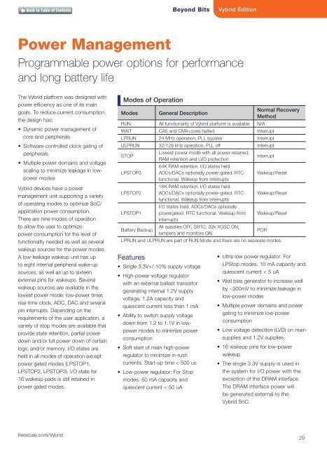
Modes of Operation<br />
Modes General Description<br />
General Description Normal Normal Recovery Recovery Method<br />
Method<br />
RUN<br />
RUN<br />
All functionality of Faraday is available<br />
All functionality of Vybrid platform is available N/A<br />
N/A<br />
WAIT CA5 and CA5 CM4 and cores CM4 Halted cores halted Interrupt Interrupt<br />
LPRUN 24MHz 24 operation, MHz operation, PLL Bypass PLL bypass Interrupt Interrupt<br />
ULPRUN<br />
ULPRUN<br />
STOP<br />
STOP<br />
LPSTOP3<br />
32/128 kHz operation, PLL off Interrupt<br />
32kHz /128kHz operation, PLL Off Interrupt<br />
Lowest power mode with all power retained,<br />
Lowest power mode with all power retained, RAM<br />
Interrupt<br />
RAM retention and LVD protection<br />
Interrupt<br />
retention and LVD protection<br />
64K RAM retention. I/O states held.<br />
64K (tbd)<br />
ADCs/DACs<br />
RAM retention.<br />
optionally<br />
I/O states held. ADCs/DACs<br />
Wake-up/Reset<br />
FPO power-gated. RTC Wakeup/Reset<br />
optionally power-gated. RTC functional. Wakeup from<br />
interrupts functional. Wakeup from interrupts<br />
LPSTOP2<br />
LPSTOP2<br />
16K RAM retention. I/O states held.<br />
16K (tbd) RAM retention. I/O states held. ADCs/DACs<br />
optionally ADCs/DACs power-gated. optionally RTC functional. power-gated. Wakeup from RTC<br />
interrupts functional. Wakeup from interrupts<br />
Wake-up/Reset<br />
Wakeup/Reset<br />
LPSTOP1 I/O states I/O states held. ADCs/DACs held. ADCs/DACs optionally powergated. optionally RTC<br />
Wake-up/Reset<br />
LPSTOP1 functional. powergated. Wakeup from RTC interrupts functional. Wakeup from Wakeup/Reset<br />
Battery All supplies interrupts OFF, SRTC, 32kXOSC ON, tampers and monitors<br />
POR<br />
Backup ON. All supplies OFF, SRTC, 32k XOSC ON,<br />
Battery Backup<br />
tampers and monitors ON.<br />
POR<br />
LPRUN and ULPRUN are part of RUN Mode and there are no separate modes.<br />
Features<br />
• Single 3.3V+/-10% supply voltage<br />
• High-power voltage regulator<br />
with an external ballast transistor<br />
generating internal 1.2V supply<br />
voltage, 1.2A capacity and<br />
quiescent current less than 1 mA<br />
• Ability to switch supply voltage<br />
down from 1.2 to 1.1V in lowpower<br />
modes to minimize power<br />
consumption<br />
• Soft start of main high-power<br />
regulator to minimize in-rush<br />
currents. Start-up time < 500 us<br />
• Low-power regulator: For Stop<br />
modes. 50 mA capacity and<br />
quiescent current < 50 uA<br />
<strong>Beyond</strong> <strong>Bits</strong> Vybrid Edition<br />
• Ultra-low power regulator: For<br />
LPStop modes. 10 mA capacity and<br />
quiescent current < 5 uA<br />
• Well bias generator to increase well<br />
by ~300mV to minimize leakage in<br />
low-power modes<br />
• Multiple power domains and power<br />
gating to minimize low-power<br />
consumption<br />
• Low voltage detection (LVD) on main<br />
supplies and 1.2V supplies<br />
• 16 wakeup pins for low-power<br />
wakeup<br />
• The single 3.3V supply is used in<br />
the system for I/O power with the<br />
exception of the DRAM interface.<br />
The DRAM interface power will<br />
be generated external to the<br />
Vybrid SoC<br />
29


