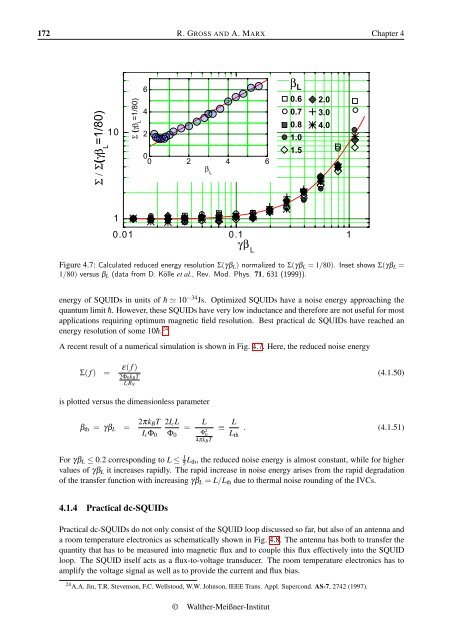
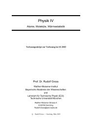
172 R. GROSS AND A. MARX Chapter 4Σ / Σ(γβ L=1/80)10Σ (γβ L=1/80)64200 2 4 6β Lβ L0.60.70.81.01.52.03.04.010.01 0.1 1Figure 4.7: Calculated reduced energy resolution Σ(γβ L ) normalized to Σ(γβ L = 1/80). Inset shows Σ(γβ L =1/80) versus β L (data from D. Kölle et al., Rev. Mod. Phys. 71, 631 (1999)).γβ Lenergy of SQUIDs in units of ¯h ≃ 10 −34 Js. Optimized SQUIDs have a noise energy approaching thequantum limit ¯h. However, these SQUIDs have very low inductance and therefore are not useful for mostapplications requiring optimum magnetic field resolution. Best practical dc SQUIDs have reached anenergy resolution of some 10¯h. 24A recent result of a numerical simulation is shown in Fig. 4.7. Here, the reduced noise energyΣ( f ) = ε( f )2Φ 0 k B TI c R N(4.1.50)is plotted versus the dimensionless parameterβ th = γβ L = 2πk BTI c Φ 02I c LΦ 0= L Φ 2 04πk B T≡LL th. (4.1.51)For γβ L ≤ 0.2 corresponding to L ≤ 1 5 L th, the reduced noise energy is almost constant, while for highervalues of γβ L it increases rapidly. The rapid increase in noise energy arises from the rapid degradationof the transfer function with increasing γβ L = L/L th due to thermal noise rounding of the IVCs.4.1.4 Practical dc-SQUIDsPractical dc-SQUIDs do not only consist of the SQUID loop discussed so far, but also of an antenna anda room temperature electronics as schematically shown in Fig. 4.8. The antenna has both to transfer thequantity that has to be measured into magnetic flux and to couple this flux effectively into the SQUIDloop. The SQUID itself acts as a flux-to-voltage transducer. The room temperature electronics has toamplify the voltage signal as well as to provide the current and flux bias.24 A.A. Jin, T.R. Stevenson, F.C. Wellstood, W.W. Johnson, IEEE Trans. Appl. Supercond. AS-7, 2742 (1997).© <strong>Walther</strong>-Meißner-<strong>Institut</strong>
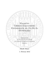
Section 4.1 APPLIED SUPERCONDUCTIVITY 173I cΦI cVantenna:signal-to-fluxconverterSQUID:flux-to-voltagetransducerelectronics:voltage amplification,bias signalsFigure 4.8: The practical dc-SQUID consisting of an antenna acting as a signal-to-flux converter, the SQUIDloop acting as the flux-to-voltage transducer, and the room temperature electronics.The Washer Type dc-SQUIDObviously, a large area A of the SQUID loop is advantageous to increase the sensitivity of a SQUID,since small field changes ∆B then result in large flux changes ∆Φ ext = A · ∆B. However, a large A alsoresults in a large loop inductance L, which may deteriorate the SQUID performance as discussed above.Based on this conflicting requirements various SQUID designs have been developed. In the 1970ies and1980ies, often three-dimensional loop geometries have been used for the realization of SQUIDs (e.g. byevaporation of a cylinder containing the Josephson junctions on a thin quartz thread).Today dc-SQUIDs are based on thin film structures, which are patterned using optical and electron beamlithography. Here, a large effective loop area at small loop inductance can be achieved by making use ofthe perfect diamagnetism of superconductors. As shown in Fig. 4.9, instead of a narrow superconductingloop structure a broad “washer-type” structure can be used. Such geometries have been successfullyused for high T c dc-SQUIDs using grain boundary Josephson junctions. 25,26,27 The washer design wasfirst proposed by M.B. Ketchen and therefore these SQUID structures today are denoted as KetchentypeSQUIDs. 28 This geometry also helps to overcome the problem of coupling the magnetic flux of theantenna system effectively to the SQUID loop of a thin film SQUID. In 1981 M.B. Ketchen and J.M.Jaycox introduced the idea of depositing a planar spiral input coil on a dc-SQUID in a square washergeometry. 29,30 The thin film planar coil is separated from the SQUID washer only by a thin insulatinglayer. A typical washer type dc-SQUID is shown schematically in Fig. 4.11. The square washer formsthe SQUID loop. It contains a narrow slit, which is closed by a superconducting line containing the twojunctions, which are located at the outer rim of the washer.For the washer geometry shown in in Figs. 4.9 and 4.11, the loop currents circulate around the inneropening (hole or slit) of the washer, which then determines the inductance of the SQUID loop. Jaycoxand Ketchen showed that a square washer with a hole of diameter D (without slit) and an outer edge W25 R. Gross et al., Appl. Phys. Lett. 57, 727 (1990).26 R. Gross et al., Physica C 170, 315 (1990).27 D. Kölle et al., Rev. Mod. Phys. 71, 631 (1999).28 M.B. Ketchen, IEEE Trans. Magn. MAG-17, 387 (1980).29 M.B. Ketchen, J.M. Jaycox, Ultra-low Noise Tunnel Junction dc-SQUID with a Tightly Coupled Planar Input Coil, Appl.Phys. Lett. 40, 736 (1982).30 J.M. Jaycox, M.B. Ketchen, Planar Coupling Scheme for Ultra-low Noise dc-SQUIDs, IEEE Trans. Magn. 17, 400 (1981).2005