

Prospects of Colloidal Nanocrystals for Electronic - Computer Science
Prospects of Colloidal Nanocrystals for Electronic - Computer Science
Prospects of Colloidal Nanocrystals for Electronic - Computer Science

Create successful ePaper yourself
Turn your PDF publications into a flip-book with our unique Google optimized e-Paper software.
<strong>Prospects</strong> <strong>of</strong> <strong>Colloidal</strong> <strong>Nanocrystals</strong> <strong>for</strong> <strong>Electronic</strong> and Optoelectronic<br />
Applications<br />
Dmitri V. Talapin,* ,†,‡ Jong-Soo Lee, † Maksym V. Kovalenko, † and Elena V. Shevchenko ‡<br />
Department <strong>of</strong> Chemistry, The University <strong>of</strong> Chicago, Chicago, Illinois 60637, and Center <strong>for</strong> Nanoscale Materials, Argonne National Lab,<br />
Argonne, Illinois 60439<br />
Contents<br />
1. Introduction 389<br />
2. Solution-Phase Synthesis <strong>of</strong> Metallic,<br />
Semiconducting, Magnetic, and Multicomponent<br />
Nanoparticles<br />
391<br />
2.1. Basics <strong>of</strong> <strong>Colloidal</strong> Synthesis: Nucleation and<br />
Growth<br />
391<br />
2.2. Nanoparticle Shape and Morphology<br />
Engineering<br />
394<br />
2.3. Multicomponent <strong>Colloidal</strong> Nanostructures 395<br />
3. Nanocrystal Solids 396<br />
3.1. Short-Range Ordered Nanoparticle Assemblies 397<br />
3.2. Nanoparticle Superlattices 397<br />
3.3. Multicomponent Nanoparticle Superstructures 398<br />
3.4. Theoretical Insight into the <strong>Electronic</strong> Structure<br />
<strong>of</strong> Nanocrystal Solids: From Insulated Dots to<br />
Three-Dimensional Minibands<br />
399<br />
4. Design <strong>of</strong> Surface Ligands 401<br />
4.1. Organic Ligands with Long Hydrocarbon<br />
Chains, Their Removal, and Exchange <strong>for</strong><br />
Smaller Molecules<br />
403<br />
4.2. Cross-Linking Surface Ligands 404<br />
4.3. Metal Chalcogenide Complexes as Surface<br />
Ligands<br />
404<br />
5. Transport in Nanocrystal Solids 405<br />
5.1. Exchange Coupling Energy 405<br />
5.2. Charging Energy 406<br />
5.3. Effects <strong>of</strong> <strong>Electronic</strong> and Structural Disorder 407<br />
5.4. Conduction Mechanisms: Hopping, VRH,<br />
ES-VRH, Cotunneling, Bloch Transport<br />
407<br />
5.5. Magnetic <strong>Nanocrystals</strong>: Spin-Dependent<br />
Transport, Magnetoresistance<br />
409<br />
5.6. Semiconductor <strong>Nanocrystals</strong>: <strong>Electronic</strong><br />
Structure and Shell Filling<br />
410<br />
5.7. Doping <strong>of</strong> Semiconductor Nanoparticles and<br />
Nanoparticle Assemblies<br />
410<br />
5.8. Multicomponent Assemblies 412<br />
6. Nanocrystal Solids <strong>for</strong> Device Applications:<br />
General Aspects<br />
412<br />
6.1. Contacts to Nanocrystal Solids 412<br />
6.2. Schottky Barriers to Nanocrystal Solids 414<br />
6.3. Effective Carrier Mobility, Lifetime, Diffusion<br />
Length, and Doping in Nanocrystal Solids:<br />
Measurement Techniques and Reported Values<br />
414<br />
* To whom correspondence should be addressed. E-mail:<br />
dvtalapin@uchicago.edu.<br />
† The University <strong>of</strong> Chicago.<br />
‡ Argonne National Lab.<br />
Chem. Rev. 2010, 110, 389–458 389<br />
Received April 5, 2009<br />
6.4. Sintering Metal and Semiconductor<br />
Nanoparticles into Continuous Films<br />
416<br />
7. Nanocrystal Devices 417<br />
7.1. Light-Emitting Devices (LEDs) 418<br />
7.1.1. LED Per<strong>for</strong>mance Characteristics 418<br />
7.1.2. Nanocrystal-Based QD-LEDs 419<br />
7.2. Photodetectors 422<br />
7.2.1. Figures <strong>of</strong> Merit <strong>for</strong> Photoconductive<br />
Detectors<br />
422<br />
7.2.2. Photoconductivity in Nanocrystal Solids 423<br />
7.2.3. Photoconductivity Measurements 424<br />
7.2.4. Photodetectors Based on Treated<br />
Nanocrystal Solids<br />
425<br />
7.2.5. Hybrid Photodetectors Using <strong>Nanocrystals</strong><br />
and Semiconducting Organic Materials<br />
426<br />
7.3. <strong>Nanocrystals</strong> in Solar Cells 426<br />
7.3.1. Per<strong>for</strong>mance Metrics and Basic Operation<br />
Principles <strong>of</strong> Solar Cells<br />
426<br />
7.3.2. <strong>Nanocrystals</strong> in Hybrid Bulk Heterojunction<br />
Solar Cells<br />
428<br />
7.3.3. <strong>Colloidal</strong> <strong>Nanocrystals</strong> <strong>for</strong> All-Inorganic<br />
Solar Cells<br />
430<br />
7.3.4. <strong>Nanocrystals</strong> in Dye-Sensitized Solar Cells 431<br />
7.3.5. Can Nanocrystal Solar Cell Beat the<br />
Shockley-Queisser Limit?<br />
432<br />
7.4. Field-Effect Transistors (FETs) 434<br />
7.4.1. Structure, Operation, and Per<strong>for</strong>mance<br />
Metrics <strong>of</strong> FETs<br />
434<br />
7.4.2. State-<strong>of</strong>-the-Art <strong>for</strong> Nanocrystal Transistors 436<br />
7.5. Memory Elements 439<br />
7.5.1. Flash Memory Devices 440<br />
7.5.2. Resistance-Change Memory Devices 443<br />
7.5.3. <strong>Nanocrystals</strong> <strong>for</strong> Magnetic Data Storage<br />
(HDDs) Applications<br />
444<br />
7.6. Nanocrystal Solids <strong>for</strong> Thermoelectric<br />
Applications: Expectations and Challenges<br />
445<br />
8. Outlook and Future Directions 448<br />
9. Acknowledgments 450<br />
10. References 450<br />
1. Introduction<br />
10.1021/cr900137k © 2010 American Chemical Society<br />
Published on Web 12/03/2009<br />
<strong>Nanocrystals</strong> (NCs) discussed in this Review are tiny<br />
crystals <strong>of</strong> metals, semiconductors, and magnetic material<br />
consisting <strong>of</strong> hundreds to a few thousand atoms each. Their<br />
size ranges from 2-3 to about 20 nm. What is special about<br />
this size regime that placed NCs among the hottest research<br />
topics <strong>of</strong> the last decades? The quantum mechanical coupling
390 Chemical Reviews, 2010, Vol. 110, No. 1 Talapin et al.<br />
Dmitri V. Talapin is an Assistant Pr<strong>of</strong>essor in the Department <strong>of</strong> Chemistry<br />
at the University <strong>of</strong> Chicago. He received his doctorate degree from the<br />
University <strong>of</strong> Hamburg, Germany, in 2002 under the supervision <strong>of</strong> Horst<br />
Weller. In 2003, he joined the IBM Research Division at the T. J. Watson<br />
Research Center as a postdoctoral fellow to work with Chris Murray on<br />
the synthesis and electronic properties <strong>of</strong> semiconductor nanostructures.<br />
In 2005, he moved to the Lawrence Berkeley National Laboratory as a<br />
staff scientist at the Molecular Foundry, newly founded DOE Center <strong>for</strong><br />
Nanoscience and Nanotechnology. In 2007, he accepted a faculty position<br />
at the University <strong>of</strong> Chicago. His research interests revolve around colloidal<br />
inorganic nanomaterials, spanning from synthetic methodology to device<br />
fabrication, with the desire <strong>of</strong> turning colloidal nanostructures into useful<br />
electronic materials.<br />
Jong-Soo Lee received a Ph.D. in the Department <strong>of</strong> Metallurgical<br />
Engineering from Chonbuk National University in South Korea in 1999.<br />
From 2001 to 2004, he worked in the Department <strong>of</strong> Electrical Engineering<br />
at Korea University in South Korea as a research assistant pr<strong>of</strong>essor. In<br />
2006-2007, he worked as a postdoctoral researcher at the Molecular<br />
Foundry in the Lawrence Berkeley National Laboratory with Dmitri V.<br />
Talapin and A. Paul Alivisatos. In 2007, he joined the Talapin group as<br />
a senior research technologist. His research interests include synthesis<br />
and charge transport studies in colloidal inorganic NCs and multifunctional<br />
nanostructures <strong>for</strong> electronic, photovoltaic, and thermoelectronic applications.<br />
<strong>of</strong> over hundreds to thousands atoms is necessary to develop<br />
the band structure <strong>of</strong> metals, semiconductors, and magnetic<br />
materials. 1-4 In this regime, the electronic structure, optical,<br />
and magnetic properties <strong>of</strong> materials can be tuned by varying<br />
the physical size <strong>of</strong> the crystal, leading to new phenomena,<br />
such as superparamagnetism <strong>of</strong> magnetic NCs, surface<br />
plasmon resonance in Au and Ag nanoparticles, 1 and the sizedependent<br />
band gap <strong>of</strong> semiconductor NCs. 2,3 These open<br />
interesting opportunities <strong>for</strong> device applications, <strong>for</strong> example,<br />
tailoring the electronic structure without introducing any<br />
changes in the chemical composition. Formerly, lithographic<br />
techniques aggressively invaded the nanoworld; nowadays,<br />
electronic circuits with features as small as 45 nm are used<br />
<strong>for</strong> commercial applications, with good prospects <strong>for</strong> 32 and<br />
Maksym V. Kovalenko received his doctorate degree from the University<br />
<strong>of</strong> Linz (Austria) in 2007 under the supervision <strong>of</strong> Pr<strong>of</strong>. Wolfgang Heiss.<br />
His doctoral thesis was focused on the synthesis and device applications<br />
<strong>of</strong> infrared-active colloidal semiconductor nanocrystals. In 2008, he joined<br />
the group <strong>of</strong> Pr<strong>of</strong>. Dmitri Talapin at the University <strong>of</strong> Chicago as a<br />
postdoctoral scholar. He is currently working on the functionalization <strong>of</strong><br />
inorganic nanocrystals with inorganic ligands and integration <strong>of</strong> these novel<br />
materials into electronic, optoelectronic, and thermoelectric devices. His<br />
other scientific interests include magnetism and self-assembly <strong>of</strong> nanocrystals.<br />
Elena V. Shevchenko received her first degree in chemistry at the<br />
Belorussian State University and her Ph.D. from the University <strong>of</strong> Hamburg<br />
in 2003 with Horst Weller. From 2003 to 2005, she was a joint postdoctoral<br />
fellow between Columbia University (with Stephen O’Brien) and the T. J.<br />
Watson Research Center IBM (with Christopher Murray). In 2005, she<br />
moved to the Molecular Foundry, Lawrence Berkeley National Laboratory,<br />
as a staff scientist. Since 2007, she is a scientist at the Center <strong>for</strong><br />
Nanoscale Materials at Argonne National Laboratory. Her primary research<br />
interests are in the design <strong>of</strong> nanoscale functional materials and<br />
understanding their fundamental properties.<br />
22 nm technologies that are on the way from laboratories to<br />
fabrication facilities. 5 Because <strong>of</strong> similarities in feature size,<br />
the knowledge obtained from electronic studies <strong>of</strong> nanoscale<br />
materials should help in understanding the design rules <strong>for</strong><br />
next generations <strong>of</strong> electronic circuits.<br />
Inorganic semiconductors have a proven track record in<br />
electronics and optoelectronics; they <strong>of</strong>fer superior carrier<br />
mobilities, light absorption, photo, and thermal stability. 5<br />
However, they are difficult to <strong>for</strong>m by low cost processes.<br />
Crystallization <strong>of</strong> inorganic semiconductors requires high<br />
temperature treatments, which <strong>for</strong>ce trade-<strong>of</strong>fs between<br />
device per<strong>for</strong>mance, fabrication costs, and compatibility with<br />
flexible plastic substrates. The development <strong>of</strong> applications<br />
ranging from photovoltaics and light-emitting devices to<br />
“smart cards”, radio frequency tags, and sensors could be<br />
accelerated by introducing lower cost alternatives to conventional<br />
technologies that rely on single crystals. 5,6 Here,
<strong>Colloidal</strong> <strong>Nanocrystals</strong> in <strong>Electronic</strong> Applications Chemical Reviews, 2010, Vol. 110, No. 1 391<br />
the nanometer size crystals can find commercial use as the<br />
building blocks <strong>for</strong> inexpensive manufacturing <strong>of</strong> low cost<br />
and large area devices. Solution-based processes such as spin<br />
coating, dip coating, or inkjet printing <strong>of</strong>fer substantial cost<br />
reductions <strong>for</strong> the fabrication <strong>of</strong> electronic and optoelectronic<br />
devices when combined with novel materials like organic<br />
semiconductors, 6,7 carbon nanotubes, 8 nanowires, 9 or hybrid<br />
organic-inorganic films. 10 Properly designed NCs can ideally<br />
fit the requirements <strong>for</strong> solution-processed electronic and<br />
optoelectronic devices because they <strong>for</strong>m thermodynamically<br />
stable and easy-to-handle colloidal solutions. Moreover, NCs<br />
can self-assemble from colloidal solutions into ordered<br />
structures called “superlattices” or “NC solids”, which will<br />
be an important subject <strong>of</strong> this review. Tunable electronic<br />
structure combined with small exciton binding energy, high<br />
luminescence efficiency, 11 and very low thermal conductivity<br />
12 make NC solids especially attractive <strong>for</strong> photovoltaic,<br />
lighting, and thermoelectric applications. Ef<strong>for</strong>ts to harness<br />
the quantum tunability <strong>of</strong> semiconductor NCs have led to<br />
many successes in optical and optoelectronic applications,<br />
such as light emitting devices, 13-16 luminescent tags, 13 and<br />
lasers. 14-16 NCs have a variety <strong>of</strong> biological and biomedical<br />
applications. 17-21 Semiconductor NCs can serve as stable<br />
fluorescence probes. 18 Magnetic NCs can be used as efficient<br />
diagnostic tools in magnetic resonance imaging and magnetic<br />
separation <strong>of</strong> biological targets 20 and therapeutic agents <strong>for</strong><br />
hyperthermic tumor treatments, 19 drug, and gene delivery. 21<br />
Plasmonic properties <strong>of</strong> noble metal NCs are utilized in<br />
molecular-specific imaging and sensing, as well as in<br />
photodiagnostic and photothermal therapy. 17<br />
At the same time, realizing solid-state electronic applications<br />
(e.g., field-effect devices) <strong>of</strong> these nanoscale building<br />
blocks has been more challenging. The confinement <strong>of</strong><br />
carriers inside the NCs imparts their fascinating size tunable<br />
properties, but, until recently, frustrated the ef<strong>for</strong>ts to<br />
efficiently contact and integrate them into devices that switch<br />
with useful speeds. 22-25 Charge transport in NCs relies on<br />
the electrons traveling between individual particles and is,<br />
there<strong>for</strong>e, dependent on the electronic communication and<br />
collective phenomena in NC arrays. In this respect, NCs are<br />
different from their cousins, nanowires and nanotubes, which<br />
can be directly connected to the electrodes.<br />
2. Solution-Phase Synthesis <strong>of</strong> Metallic,<br />
Semiconducting, Magnetic, and Multicomponent<br />
Nanoparticles<br />
<strong>Colloidal</strong> synthesis <strong>of</strong> inorganic nanostructures is developing<br />
into a new branch <strong>of</strong> synthetic chemistry. Starting with<br />
preparations <strong>of</strong> simple objects like monodisperse spherical<br />
nanoparticles, 26-29 the field is now moving toward more and<br />
more sophisticated structures where size, shape, and connectivity<br />
<strong>of</strong> multiple parts <strong>of</strong> a multicomponent structure can<br />
be tailored in an independent and predictable manner. 30-36<br />
Many technologically important metals, semiconductors, and<br />
magnetic materials can be synthesized as uni<strong>for</strong>m sub-20<br />
nm crystals; multiple materials can be combined in the <strong>for</strong>m<br />
<strong>of</strong> the core-shell, dumbbell, or more complex morphologies.<br />
37 Although the general methodology <strong>of</strong> colloidal<br />
synthesis <strong>of</strong> multicomponent structures is much less developed<br />
as compared to the conventional synthesis <strong>of</strong> molecular<br />
compounds, impressive progress has been achieved in the<br />
past years, which introduced totally novel approaches to<br />
materials design. For example, the band gap <strong>of</strong> semiconduc-<br />
tor nanostructures can be precisely tuned by size and shape<br />
control, electron and hole can be spatially separated within<br />
the NC by introducing heterostructures with staggered band<br />
<strong>of</strong>fsets, 35 different confined regimes can be achieved <strong>for</strong><br />
electrons and holes, 33 etc. Growing heterostructures built <strong>of</strong><br />
semiconductor and plasmonic materials allow coupling<br />
excitons and surface plasmon resonance generated by<br />
semiconductor and metal components, respectively. 24,38 Below,<br />
we briefly describe the methodology <strong>of</strong> colloidal<br />
synthesis. For more detailed in<strong>for</strong>mation, we should address<br />
the readers to numerous comprehensive reviews on the<br />
synthesis <strong>of</strong> inorganic nanomaterials. 28,37,39-45<br />
2.1. Basics <strong>of</strong> <strong>Colloidal</strong> Synthesis: Nucleation<br />
and Growth<br />
Among the appeals <strong>of</strong> solution-based colloidal synthesis,<br />
we should mention the excellent control over size and shape<br />
<strong>of</strong> prepared nanostructures and applicability to a broad range<br />
<strong>of</strong> materials. Moreover, the use <strong>of</strong> relatively simple experimental<br />
equipment and chemicals allows one to obtain highquality<br />
materials and tailor their properties at surprisingly<br />
low cost. 46 Typically, colloidal nanomaterials are synthesized<br />
by reacting appropriate molecular precursors, that is, inorganic<br />
salts or organometallic compounds. The colloidal<br />
synthesis generally involves several consecutive stages:<br />
nucleation from initially homogeneous solution, growth <strong>of</strong><br />
the pre<strong>for</strong>med nuclei, isolation <strong>of</strong> particles reaching the<br />
desired size from the reaction mixture, postpreparative<br />
treatments, etc. As a rule, temporal separation <strong>of</strong> the<br />
nucleation event from the growth <strong>of</strong> the nuclei is required<br />
<strong>for</strong> narrow size distribution. 26,47,48 The so-called hot-injection<br />
technique, when the precursors are rapidly injected into a<br />
hot solvent with subsequent temperature drop, satisfies this<br />
requirement. 26,48,49 The separation <strong>of</strong> nucleation and growth<br />
stages can also be achieved upon steady heating <strong>of</strong> the<br />
reaction mixture. 46<br />
Nucleation and growth <strong>of</strong> NCs occurs in the solution phase<br />
in the presence <strong>of</strong> organic surfactant molecules, which<br />
dynamically adhere to the surface <strong>of</strong> growing crystals. 30,46<br />
Typical surfactants include long-chain carboxylic and phosphonic<br />
acids (e.g., oleic acid and n-octadecylphosphonic<br />
acid), alkanethiols (e.g., dodecanethiol), alkyl phosphines,<br />
alkylphosphine oxides (classical examples are trioctylphosphine,<br />
TOP, and trioctylphosphine oxide, TOPO), and<br />
alkylamines such as hexadecylmine. The surfactant molecules<br />
play the key role in tuning the kinetics <strong>of</strong> nucleation and<br />
growth, 39,47 which should be kinetically balanced because if<br />
the nanoparticle nucleation rate is either too slow or too fast<br />
with respect to the growth rate, the reaction will generate<br />
either bulk crystals or molecular clusters. Achieving proper<br />
balance <strong>of</strong> these intrinsically different processes is an<br />
important and sometimes challenging problem, which is<br />
usually addressed empirically by searching <strong>for</strong> a good<br />
combination <strong>of</strong> molecular precursors, surfactants, solvent,<br />
and the reaction conditions (temperature regime, etc.).<br />
Development <strong>of</strong> reproducible synthetic approaches leading<br />
to nanoparticles with uni<strong>for</strong>m size, shape, composition, and<br />
surface morphology is extremely important <strong>for</strong> further<br />
progress in fundamental studies and practical applications.<br />
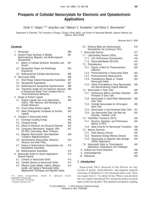
Figure 1 shows several examples <strong>of</strong> metal nanocrystals<br />
synthesized by colloidal chemistry. Metal nanoparticles can<br />
be synthesized by reducing the metal ions using reductant<br />
such as borohydride, amines, or 1,2-diols in the presence <strong>of</strong><br />
stabilizing agents, typically long-chain alkanethiols (e.g.,
392 Chemical Reviews, 2010, Vol. 110, No. 1 Talapin et al.<br />
Figure 1. Examples <strong>of</strong> colloidally synthesized metal and metal<br />
alloy nanoparticles.<br />
dodecanethiol), amines, or fatty acids. This approach works<br />
quite well <strong>for</strong> noble metals (Au, 50-53 Ag, 54-56 Pt, 57-59 Pd 60 )<br />
and their alloys (e.g., Au-Ag 61 ). Current developments in<br />
the synthesis <strong>of</strong> these materials have been extensively<br />
reviewed by Xia et al., 44 Yang et al., 62 and Liz-Marzan. 63<br />
More reactive transition and main group metals (Co, 4,64<br />
Fe, 4,65-67 Cr, 68 Bi, 69 Pb 70 ) require rigorous control <strong>of</strong> the<br />
reaction conditions and are synthesized under inert atmosphere.<br />
High temperatures, up to 300 °C, are <strong>of</strong>ten necessary<br />
to anneal out the defects in crystalline lattice and <strong>for</strong>m highly<br />
crystalline particles. 47 High boiling solvents are used to<br />
provide a wide window <strong>of</strong> reaction temperatures. The choice<br />
<strong>of</strong> solvent limits the range <strong>of</strong> possible molecular precursors.<br />
For example, solvents with low polarity such as dioctyl ether<br />
or 1-octadecene require precursors soluble in this medium.<br />
Among metal salts, acetylacetonates or carboxylates are<br />
frequently used 27,29,47 in the synthesis <strong>of</strong> metal nanoparticles.<br />
Alternatively, metal NCs can be generated by thermal<br />
decomposition <strong>of</strong> molecules containing zerovalent metal,<br />
such as metal carbonyls. 4,27,47 For example, cobalt nanoparticles<br />
can be synthesized either by reduction <strong>of</strong> Co(II) ions<br />
in solution or by thermal decomposition <strong>of</strong> Co2(CO)8. 4 Longchain<br />
carboxylic acids or alkylamines are the typical surfactants<br />
<strong>for</strong> metal NCs. In addition to size and shape,<br />
precursors and surfactants can control the crystalline phase<br />
<strong>of</strong> the nanoparticle. Thus, three different polymorphs <strong>of</strong><br />
cobalt NCs (hexagonal close-packed, face-centered cubic,<br />
and epsilon phase) were selectively synthesized by adjusting<br />
reaction parameters. 47 Combining two or more metal precursors,<br />
<strong>for</strong> example, Pt(acac)2 and Fe(CO)5, in a one-pot<br />
reaction allows one to obtain nanoparticles <strong>of</strong> metal alloys. 27,71<br />
Among a variety <strong>of</strong> possible metal combinations, the alloys<br />
<strong>of</strong> magnetic metals (Fe, Co, and Ni) with Pt and Pd have<br />
been studied most extensively because in these systems<br />
alloying helped to overcome a serious drawback <strong>of</strong> elemental<br />
magnetic nanoparticles, their low stability against oxidation.<br />
Several methods can be used to tune the size <strong>of</strong> metal<br />
nanoparticles during synthesis. Usually, the metal nanoparticles<br />
nucleate and grow very quickly, and it is difficult to<br />
terminate the reaction at the desired stage <strong>of</strong> particle growth.<br />
Instead, the particle size can be adjusted by first making small<br />
nanoparticles, which are then used as seeds <strong>for</strong> further growth<br />
by adding controllable amounts <strong>of</strong> molecular precursors. For<br />
example, this method was applied to vary the size <strong>of</strong> FePt27 NCs. Another approach is based on tuning the relative rates<br />
<strong>of</strong> nanoparticle nucleation and growth. If the total amount<br />
<strong>of</strong> molecular precursors used in the reaction is constant, the<br />
fast nucleation provides high concentration <strong>of</strong> nuclei and<br />
yields smaller NCs. Instead, slow nucleation provides low<br />
concentration <strong>of</strong> seeds consuming the same amount <strong>of</strong><br />
precursors, thus resulting in larger particles. 47 The balance<br />
between nucleation and growth rates can be tuned via<br />
changing <strong>of</strong> the reaction temperature because the activation<br />
energy <strong>for</strong> the homogeneous nucleation is usually much<br />
higher than that <strong>for</strong> particle growth. 72 Typically, the increase<br />
<strong>of</strong> reaction temperature allowed one to obtain smaller NCs<br />
<strong>for</strong> different materials. 47 Besides the reaction temperature,<br />
there are a number <strong>of</strong> other methods to control particle size,<br />
such as nature and concentration <strong>of</strong> capping molecules, molar<br />
ratios <strong>of</strong> precursors, etc. For example, lowering the concentration<br />
<strong>of</strong> surfactants in reaction mixture can also lead to<br />
smaller nanoparticles. 47<br />
Significant success was achieved in the synthesis <strong>of</strong> NCs<br />
<strong>of</strong> different technologically important semiconductors. Some<br />
examples <strong>of</strong> colloidal semiconductor NCs are shown in<br />
Figure 2. Typical reactions used <strong>for</strong> the synthesis <strong>of</strong> II-VI<br />
(CdSe, CdTe, CdS), 26,49,73-77 III-V (InP, InAs), 78-81 and<br />
IV-VI (PbS, 82-86 PbSe, 23 PbTe87 ) semiconductor NCs are<br />
outlined by reactions 1-3. The syntheses are carried out at<br />
high temperatures, and in the presence <strong>of</strong> long-chain alkylphosphines<br />
(e.g., trioctylphosphine, TOP), alkylphosphine<br />
oxides (e.g., trioctylphosphine oxide, TOPO), alkylamines<br />
(e.g., hexadecylamine, HDA), and alkylphosphonic acids as<br />
the stabilizing agents.<br />
300°C, HDA-TOPO-TOP<br />
Cd(CH3 ) 2 + (C8H17 ) 3PSe98 CdSe nanocrystals (1)<br />
260°C, TOP<br />
InCl3 + [(CH3 ) 3Si] 3P98 InP nanocrystals (2)<br />
180°C, oleic acid<br />
Pb(CH3COO) 2 + (C8H17 ) 3PSe98 PbSe nanocrystals (3)<br />
In many cases, the size <strong>of</strong> semiconductor NCs can be tuned<br />
by adjusting the concentrations <strong>of</strong> surfactants, reaction<br />
temperature, and duration <strong>of</strong> the particle growth. In a
<strong>Colloidal</strong> <strong>Nanocrystals</strong> in <strong>Electronic</strong> Applications Chemical Reviews, 2010, Vol. 110, No. 1 393<br />
Figure 2. Examples <strong>of</strong> colloidal semiconductor nanocrystals <strong>of</strong><br />
different materials.<br />
colloidal solution, semiconductor NCs <strong>of</strong>ten grow through<br />
the Ostwald ripening mechanism, where the largest particles<br />
in solution grow at the expense <strong>of</strong> dissolving smaller ones.<br />
As a result, average particle size increases with time, 72 and<br />
the particle concentration decreases. A number <strong>of</strong> studies<br />
investigated the kinetics <strong>of</strong> nanoparticle growth and dissolution<br />
to model this self-consistent growth process and<br />
understand the parameters that control particle size distribution<br />
during the synthesis <strong>of</strong> semiconductor NCs. 80 Two<br />
regimes, so-called “focusing” and “defocusing” <strong>of</strong> size<br />
distribution during nanoparticle growth, were described by<br />
Peng et al. 88,89 “Nano-Ostwald ripening” model was proposed<br />
to describe the evolution <strong>of</strong> an ensemble <strong>of</strong> nanoscale<br />
particles. 90<br />
One <strong>of</strong> the most important manifestations <strong>of</strong> quantum<br />
confinement in semiconductors is the relationship between<br />
the electronic structure and particle size. 2,3 In semiconductor<br />
NCs, it gives rise to discrete electron and hole states that<br />
can be precisely tuned by varying particle size (Figure 3). 2,3<br />
The proper control <strong>of</strong> surface chemistry can eliminate the<br />
midgap states associated with surface dangling bonds. As a<br />
result <strong>of</strong> reduced probability <strong>of</strong> carrier trapping and nonradiative<br />
recombination, high (>80%) luminescence quantum<br />
efficiencies were achieved <strong>for</strong> semiconductor NCs. 11,91-94<br />
Discussion <strong>of</strong> solution-phase synthesis <strong>of</strong> inorganic nanomaterials<br />
would be incomplete without mentioning other<br />
methodologies, complementary to above-described hightemperature<br />
synthesis in nonpolar organic solvents. Thus,<br />
there are several examples <strong>of</strong> high-quality semiconductor<br />
nanoparticles synthesized in aqueous medium. 96-98 For<br />
example, quite monodisperse samples <strong>of</strong> highly luminescent<br />
CdTe NCs can be prepared by reacting a cadmium salt (e.g.,<br />
cadmium perchlorate) with H2Te gas in aqueous solution<br />
containing thiol molecules with polar groups (e.g., thiogly-<br />
Figure 3. Size-dependent change <strong>of</strong> the emission color <strong>for</strong> colloidal<br />
solutions <strong>of</strong> CdSe/ZnS core-shell nanocrystals. The particles with<br />
the smallest (∼1.7 nm) CdSe core emit blue; the particles with the<br />
largest (∼5 nm) core emit red. Reprinted with permission from<br />
reference 95. Copyright 2002 Wiley.<br />
colic acid, cysteamine). It is commonly accepted that the<br />
thiol group binds to the NC surface, whereas the deprotonated<br />
carboxylic group (or protonated amino group) provides<br />
colloidal stability due to electrostatic repulsion <strong>of</strong> charged<br />
NCs. 96,99 This approach has been successfully applied to<br />
different II-VI semiconductors: CdS, 100 CdSe, 101 CdTe, 102<br />
HgTe, 103 etc. Generally, the NCs made in aqueous medium<br />
are not as monodisperse as those prepared in organic<br />
solvents, but in other aspects, such as luminescence efficiency,<br />
colloidal stability, and, especially, cost per gram,<br />
they can be very competitive. We may expect a revival <strong>of</strong><br />
interest in the aqueous synthesis <strong>of</strong> colloidal NCs <strong>for</strong> largescale<br />
manufacturing purposes.<br />
The other prominent methodology is the so-called sol-gel<br />
technique that has been widely studied as one <strong>of</strong> the most<br />
popular routes <strong>for</strong> synthesis <strong>of</strong> oxide materials. 104,105 Typical<br />
precursors <strong>for</strong> sol-gel process are metal alkoxides and metal<br />
chlorides, which undergo hydrolysis and polycondensation<br />
reactions to <strong>for</strong>m a colloid. Traditional sol-gel processes<br />
include a series <strong>of</strong> hydrolysis and condensation reactions <strong>of</strong><br />
the precursors in acidic or basic aqueous or alcohol media,<br />
<strong>for</strong>ming first nanoparticles (colloidal sols) controllably aggregating<br />
into a wet network (gel). The sol-gel process can<br />
be divided into several stages: (i) <strong>for</strong>mation <strong>of</strong> stable<br />
solutions <strong>of</strong> the metal alkoxide (the sol); (ii) gelation resulting<br />
from the <strong>for</strong>mation <strong>of</strong> an oxide- or alcohol-bridged network<br />
by a polycondensation reaction (the gel); (iii) aging <strong>of</strong> the<br />
gel (syneresis) accompanied by contraction <strong>of</strong> the gel<br />
network and expulsion <strong>of</strong> solvent from the gel pores; (iv)<br />
drying to remove water and other volatile liquids from the<br />
gel network; (v) dehydration <strong>for</strong> removing surface-bound<br />
M-OH groups; and (vi) thermal decomposition <strong>of</strong> the gels<br />
at high temperatures. From this process, the pores <strong>of</strong> the gel<br />
network are collapsed, and the remaining organic precursors<br />
are decomposed.<br />
Depending upon how the wet gel is dried, the density and<br />
extent <strong>of</strong> porosity <strong>of</strong> the network can be effectively tuned,<br />
consequently impacting the bulk physical properties. Solvent<br />
removal can have a huge effect on the gel structure and is a<br />
critical step <strong>for</strong> creating nanostructures with desired functionality.<br />
106 During thermal drying or room-temperature<br />
solvent evaporation, capillary <strong>for</strong>ces induce stresses on the<br />
gel that induce collapse <strong>of</strong> the network, eventually leading<br />
to so-called xerogels with a collapsed but still porous <strong>for</strong>m<br />
<strong>of</strong> the original gel network. On the other hand, the supercritical<br />
extraction <strong>of</strong> solvent from a gel does not induce<br />
capillary stresses due to the lack <strong>of</strong> solvent-vapor inter-
394 Chemical Reviews, 2010, Vol. 110, No. 1 Talapin et al.<br />
faces. 106 Obtained aerogels retain a much stronger resemblance<br />
to their original gel network structure than do<br />
xerogels. For more details on sol-gel synthesis, we address<br />
the reader to several recent review articles. 105,107-111<br />
Brock et al. reported the synthesis <strong>of</strong> xerogels and aerogels<br />
assembled from CdS, ZnS, PbS, CdSe, and CdSe/ZnS core/<br />
shell nanoparticles. 112,113 Primary nanoparticles were aggregated<br />
to the wet gels and then dried under ambient<br />
conditions or in supercritical CO2 to produce nanoparticle<br />
xerogels and aerogels, respectively.<br />
2.2. Nanoparticle Shape and Morphology<br />
Engineering<br />
In analogy with bulk crystals, the nanoparticles are<br />
terminated by facets that expose different crystallographic<br />
planes. Selective adhesion <strong>of</strong> surfactant molecules allows <strong>for</strong><br />
tuning the growth kinetics <strong>of</strong> different crystal facets and<br />
tailoring the NC shape from nearly spherical to highly<br />
anisotropic 30 (Figure 4). Strong binding <strong>of</strong> capping molecules<br />
suppresses the growth <strong>of</strong> certain facets, leading to a variety<br />
<strong>of</strong> NC shapes. The multicomponent mixtures <strong>of</strong> stabilizing<br />
agents are <strong>of</strong>ten employed to provide the difference in growth<br />
rate in different crystallographic directions. For example,<br />
depending on the length <strong>of</strong> alkyl chain and concentration <strong>of</strong><br />
alkylphosphonic acid and the heating regime, the rod-,<br />
arrow-, rise-, teardrop-, and tetrapod-shaped CdSe NCs can<br />
be synthesized. 4,32 Possible nanoparticle shapes are determined<br />
by symmetry <strong>of</strong> underlying crystal lattice; <strong>for</strong> example,<br />
PbSe NCs with rocksalt atomic lattice can be synthesized in<br />
the <strong>for</strong>m <strong>of</strong> spheres, cubes (Figure 4a), octahedrons, or starshaped<br />
NCs. 31<br />
Tetrapods <strong>of</strong> ZnO, 114 iron oxide, 115 Pt, 116 CdSe, 35,117,118<br />
CdTe (Figure 4b), 119 ZnSe, 120,121 and ZnS 121 are the examples<br />
<strong>of</strong> nanomaterials with higher level <strong>of</strong> morphological complexity.<br />
Two models were adopted to explain the <strong>for</strong>mation<br />
Figure 4. Examples <strong>of</strong> inorganic nanomaterials with different<br />
shapes and morphologies synthesized by colloidal chemistry:<br />
(a) PbSe cubes; 31 (b) CdTe tetrapods; 119 (c) PbSe nanowires; 31 and<br />
(d) hollow iron oxide nanoparticles. Reprinted with permission<br />
from ref 31. Copyright 2005 American Chemical Society. Reprinted<br />
with permission from ref 119. Copyright 2003 Nature Publishing<br />
Group.<br />
<strong>of</strong> the tetrapods. The nucleation <strong>of</strong> seeds with zinc-blende<br />
crystal structure followed by the growth <strong>of</strong> four wurtzitephase<br />
arms was originally proposed to explain the morphology<br />
<strong>of</strong> CdTe nanotetrapods. 117,119,122 The alternative octahedral<br />
multiple twin model is based on the assumption that<br />
the center <strong>of</strong> tetrapod consists <strong>of</strong> eight tetrahedral domains<br />
enclosed by low-index, high-atomic-density planes and three<br />
twin planes at the common edges. 114,121,123-125 The further<br />
growth <strong>of</strong> octa-twin core results in decohesion <strong>of</strong> the twin<br />
boundaries to relieve the strain energy accumulated at the<br />
common edges <strong>of</strong> the twins. Preferential growth along the<br />
c-axis <strong>for</strong> wurzite domains leads to the <strong>for</strong>mation <strong>of</strong> a<br />
tetrapod. Formation <strong>of</strong> the twin planes is also known to be<br />
a reason <strong>of</strong> complex faceting and unusual anisotropic<br />
structures <strong>for</strong> noble metal nanostructures, <strong>for</strong> example, Au<br />
and Ag nanowires with 5-fold cross sections. 126<br />
There are a number <strong>of</strong> other techniques that can be applied<br />
to engineer the shape <strong>of</strong> colloidal NCs. Thus, long uni<strong>for</strong>m<br />
colloidal nanowires (Figure 4c) can be synthesized by the<br />
oriented attachment 127-130 or solution-liquid-solid 131 growth<br />
mechanisms. In oriented attachment, individual nanoparticles<br />
attach and fuse along identical crystal faces <strong>for</strong>ming oriented<br />
chains. 128 Such anisotropic assembly along one direction<br />
followed by subsequent fusion and annealing <strong>of</strong> surface<br />
defects has been reported <strong>for</strong> a number <strong>of</strong> systems including<br />
Ag, 132 CdTe, 133 CdSe, 134 PbSe, 31 ZnO, 135 ZnS, 136 ZnTe, 137<br />
and In2O3. 138 To explain anisotropic growth, the concept <strong>of</strong><br />
dipole-dipole interparticle interactions as a driving <strong>for</strong>ce <strong>of</strong><br />
chain <strong>for</strong>mation was proposed. 31,127,133 Synthesis through the<br />
oriented attachment allows one to control the nanowire<br />
morphology. In addition to straight wires, zigzag, helical,<br />
branched, and tapered nanowires could all be prepared by<br />
adjustment <strong>of</strong> the reaction conditions. 31 Solution liquid solid<br />
growth (SLS) <strong>of</strong> nanowires 131,139 involves the stages analogous<br />
to vapor-liquid-solid growth, 140-142 but nanowires<br />
grow in a colloidal solution in the presence <strong>of</strong> surfactant<br />
molecules, which prevent aggregation and precipitation <strong>of</strong><br />
nanowires. In this approach, metal nanoparticles are used as<br />
catalysts to initiate and direct the nanowire growth; the droplets<br />
<strong>of</strong> melted metal function as a liquid phase catalyst <strong>for</strong> the growth<br />
<strong>of</strong> solid phase through intermediate <strong>for</strong>mation <strong>of</strong> supersaturated<br />
eutectic solution <strong>of</strong> semiconductor in metal. 131 Nanoparticles<br />
<strong>of</strong> low-melting point metals such as Bi or In were used as<br />
the catalysts <strong>for</strong> solution-phase synthesis <strong>of</strong> different group<br />
IV, II-VI, III-V, and IV-VI semiconductor nanowires,<br />
freely suspended in solution. 139,143-146<br />
Hollow nanomaterials (Figure 4d) were synthesized through<br />
the nanoscale Kirkendall effect based on the difference in<br />
diffusion rates <strong>of</strong> two species resulting in accumulation and<br />
condensation <strong>of</strong> vacancies. 147 During gentle oxidation <strong>of</strong><br />
metal nanoparticles, the outward diffusion <strong>of</strong> metal is much<br />
faster in <strong>for</strong>med oxide layer than the inward diffusion <strong>of</strong><br />
oxygen, leading to the <strong>for</strong>mation <strong>of</strong> a nanoscale void in the<br />
center <strong>of</strong> a nanoparticle. 148 This phenomenon was originally<br />
discovered by Yin et al. 148 and was observed <strong>for</strong> a variety<br />
<strong>of</strong> materials including hollow magnetic iron oxide (Figure<br />
4d) 149 and cobalt sulfide 148 nanoparticles. Galvanic displacement<br />
reactions have been also employed <strong>for</strong> the synthesis<br />
<strong>of</strong> hollow nanostructures. 150 Thus, Xia et al. reported the<br />
<strong>for</strong>mation <strong>of</strong> hollow Au nanoboxes by reacting ∼100 nm<br />
Ag cubes with Au 3+ ions. 151,152 The hollow Au structure<br />
<strong>for</strong>med because in the course <strong>of</strong> galvanic displacement<br />
reduction <strong>of</strong> each Au 3+ ion required the oxidation and<br />
dissolution <strong>of</strong> three silver atoms in the nanoparticle core.
<strong>Colloidal</strong> <strong>Nanocrystals</strong> in <strong>Electronic</strong> Applications Chemical Reviews, 2010, Vol. 110, No. 1 395<br />
Formation <strong>of</strong> hollow Au NCs allowed one to engineer their<br />
optical properties because the frequency <strong>of</strong> surface plasmon<br />
resonance in a hollow NC was strongly dependent on the<br />
shell thickness and shape. 153<br />
2.3. Multicomponent <strong>Colloidal</strong> Nanostructures<br />
One <strong>of</strong> the most exciting aspects <strong>of</strong> colloidally synthesized<br />
nanomaterials is the possibility to prepare various multicomponent<br />
nanostructures. Combining materials at the nanoscale<br />
opens up additional opportunities <strong>for</strong> manipulating<br />
wave functions, Plasmon resonances, spins, and other materials<br />
properties. 36,37,154 Thus, bringing together components <strong>of</strong><br />
intrinsically different functionality constitutes a particularly<br />
powerful route to creating novel functional materials with<br />
synergetic properties found in neither <strong>of</strong> the constituents.<br />
Multicomponent nanostructures can be prepared via multistep<br />
syntheses where presynthesized NCs are used as seeds <strong>for</strong><br />
nucleation and growth <strong>of</strong> other inorganic phase. Significant<br />
progress has been achieved in the synthesis <strong>of</strong> core-shell<br />
NCs combining two different semiconductors, 49,94,155-157<br />
metals, 158,159 or a metal and a semiconductor160 in the <strong>for</strong>m<br />
<strong>of</strong> a concentric core and shell (Figure 5a). Such morphology<br />
can be obtained by growing a uni<strong>for</strong>m layer <strong>of</strong> a shell<br />
material around colloidal particles. In the case <strong>of</strong> epitaxial<br />
semiconductor-semiconductor core-shell NCs, the choice<br />
<strong>of</strong> materials <strong>for</strong> the core and the shell allows <strong>for</strong> controlling<br />
the confinement <strong>of</strong> electron and hole wave functions, which,<br />
in turn, determines their optical and electronic properties. If<br />
a narrow gap semiconductor is covered by a shell <strong>of</strong> semiconductor<br />
with wide band gap, both electron and hole wave<br />
functions will be strongly confined to the core (Figure 5b,<br />
left). This confinement regime called type-I heterostructure<br />
is observed, <strong>for</strong> example, in CdSe/ZnS, 49,155 InAs/ZnSe, 161,162<br />
InP/ZnS, 163 and other systems. It is favorable <strong>for</strong> achieving<br />
high quantum efficiency and stability <strong>of</strong> photo- and elec-<br />
Figure 5. (a) Structure <strong>of</strong> a core-shell nanocrystal optimized <strong>for</strong><br />
high luminescence efficiency and stability. Reproduced with<br />
permission from ref 171. (b) Schematic representation <strong>of</strong> the band<br />
structure <strong>of</strong> (left) CdSe/ZnS, (middle) CdSe/CdS, and (right) CdTe/<br />
CdSe core shell nanocrystals. The radial probability functions <strong>for</strong><br />
the lowest energy electron and hole wave functions are schematically<br />
shown as red and blue curves, respectively. (c) An example<br />
<strong>of</strong> a nanostructure where electron and hole have different confinement<br />
regimes: the electron and hole are confined in two and three<br />
dimensions, respectively.<br />
Figure 6. TEM images showing different examples <strong>of</strong> multicomponent<br />
nanostructures: (a) CdSe/CdS nanorods; 33,34 (b) CdSe/CdS<br />
tetrapods; 33 (c) Au/PbS core-shells; 24 (d) CoPt3-Au dumbbells; 174<br />
(e) Au-CdSe-Au rods; 38 (f) CdS-Au2S segmented nanoheterostructures.<br />
175 (a,b) Reprinted with permission from ref 33. Copyright<br />
2007 American Chemical Society. (c) Reprinted with permission<br />
from ref 24. Copyright 2008 American Chemical Society. (e)<br />
Reprinted with permission from ref 38. Copyright 2004 American<br />
Association <strong>for</strong> Advancement <strong>of</strong> <strong>Science</strong>. (f) Reprinted with<br />
permission from ref 175. Copyright 2007 American Association<br />
<strong>for</strong> Advancement <strong>of</strong> <strong>Science</strong>.<br />
troluminescence, protecting emitting core from oxidation. In<br />
some cases, the band gap <strong>of</strong> the shell material is not wide<br />
enough to confine both electron and hole wave functions.<br />
For example, in CdSe/CdS core-shell NCs, electron can<br />
freely move between CdSe and CdS phases, whereas the hole<br />
is confined to the CdSe core because <strong>of</strong> its large effective<br />
mass and substantial <strong>of</strong>fset <strong>of</strong> the valence band energies<br />
(Figure 5b, middle). It is possible to independently engineer<br />
symmetry <strong>of</strong> electron and hole wave functions by varying<br />
shapes <strong>of</strong> CdSe and CdS parts <strong>of</strong> the nanostructure. For<br />
example, one can prepare nanomaterials <strong>of</strong> “mixed dimensionality”<br />
with three-dimensionally confined holes and twodimensionally<br />
confined electrons (Figures 5c and 6a). 33,34,164<br />
Different behavior is observed when core and shell <strong>for</strong>m<br />
heterostructure with staggered band <strong>of</strong>fset (Figure 5b, right),<br />
the so-called type-II heterostructure. 165-167 In the lowest<br />
excited state, the electron and hole wave functions are<br />
spatially separated, slowing the radiative recombination rate<br />
and facilitating separation <strong>of</strong> photogenerated carriers. 167<br />
Chemically synthesized type-II nanoheterostructures are<br />
considered promising candidates <strong>for</strong> photovoltaic 168 and
396 Chemical Reviews, 2010, Vol. 110, No. 1 Talapin et al.<br />
lasing 16 applications. The confinement regime can depend<br />
on the diameter <strong>of</strong> the core and thickness <strong>of</strong> the shell. For<br />
example, ZnSe/CdSe core-shell nanoparticles can exhibit<br />
either type-I or type-II behavior, depending on CdSe shell<br />
thickness. 165,169 If core and shell materials have a difference<br />
in lattice parameters (i.e., lattice mismatch) larger than a few<br />
percent, the addition <strong>of</strong> an intermediate “wetting” layer helps<br />
to relax the interfacial strain and prevent accumulation <strong>of</strong><br />
structural defects at the interface. 11,170<br />
The seeded growth can be used to fabricate a large variety<br />
<strong>of</strong> core-shell structures, including some very unusual<br />
material combinations such as Co/CdSe, 160 FePt/CdSe, 172<br />
PtFe/CdS 172 magnetic core-semiconductor shell, or Au/PbS<br />
plasmonic core-semiconductor shell 24 (Figure 6c). Depending<br />
on the interfacial energy, lattice matching, and the<br />
reaction conditions, multicomponent nanostructures can range<br />
from uni<strong>for</strong>mly covered core-shells to dumbbells (Figure<br />
6d) and even highly anisotropic heterostructures like tetrapods<br />
shown in Figure 6b.<br />
The use <strong>of</strong> seeds other than spherical nanoparticle, such<br />
as nanorods and tetrapods, may result in highly anisotropic<br />
structures where the new phase is selectively deposited on<br />
the tips <strong>of</strong> nanorods or tetrapod arms. Thus, PbSe/CdSe/<br />
PbSe, 173 CdTe/CdSe/CdTe, 35 and metal-semiconductor-metal<br />
Au/CdSe/Au heterostructures 38 (Figure 6e) were synthesized<br />
from CdSe nanorods.<br />
Robinson et al. used partial exchange <strong>of</strong> Cd 2+ ions in CdS<br />
nanorods with Ag + via cation exchange reaction 175 to prepare<br />
beautiful periodic CdS/Ag2S nanoheterostructures (Figure 6f).<br />
This approach is considered as a promising route to create<br />
modulated structures, interesting <strong>for</strong> thermoelectronic applications.<br />
Among other examples <strong>of</strong> multicomponent nanostructures,<br />
Au/PbS, 24 CoPt3/Au dumbbells, 174 PbSe/Aux, 176<br />
gold/iron oxide dumbbells, 177 solid core-shell 178 and<br />
core-hollow shell structures, 32 TiO2/Fe2O3, 179 PtFe/iron<br />
oxide, 180 and ZnO/Ag, 181 and many others have been reported<br />
during the last several years. The recent advances in the<br />
synthesis <strong>of</strong> hybrid structures were reviewed by Cozzoli et<br />
al. 37 and Zeng et al. 36<br />
The toolbox <strong>of</strong> synthetic techniques is quickly expanding,<br />
and many novel structures are reported every year. No doubt,<br />
this progress will further continue, providing scientists and<br />
engineers with novel potential functional building blocks <strong>for</strong><br />
electronics and optoelectronics.<br />
3. Nanocrystal Solids<br />
When considering chemically synthesized nanoparticles<br />
<strong>for</strong> electronic and optoelectronic applications, we should keep<br />
in mind that the actual active element <strong>of</strong> most devices will<br />
be not individual nanoparticles but their macroscopic arrays.<br />
In analogy with conventional solids, the assemblies <strong>of</strong><br />
nanoparticles should conduct charge carriers and per<strong>for</strong>m<br />
other useful actions such as light absorption and carrier<br />
separation in solar cells, light emission in LEDs, etc. The<br />
ability to tailor size, shape, and compositions <strong>of</strong> individual<br />
nanoparticles provides means <strong>for</strong> fine-tuning material properties.<br />
At the same time, the behavior <strong>of</strong> nanoparticle ensembles<br />
depends not only on the properties <strong>of</strong> individual elements,<br />
but on the electronic and optical communication between<br />
the nanoparticles, on the interparticle medium, packing<br />
density, and mutual orientations <strong>of</strong> NCs, etc. All <strong>of</strong> these<br />
issues add new levels <strong>of</strong> complexity to the problem <strong>of</strong><br />
designing electronic materials from nanoparticle building<br />
blocks. At the same time, understanding and utilizing self-<br />
Figure 7. (a) High-resolution cross-section SEM image <strong>of</strong> a dropcast<br />
film assembled from PbSe nanocrystals. Thickness <strong>of</strong> SiO2<br />
layer is 100 nm. Reprinted with permission from ref 23. Copyright<br />
2005 American Association <strong>for</strong> Advancement <strong>of</strong> <strong>Science</strong>. (b) SEM<br />
micrographs <strong>of</strong> a glassy solid prepared from 5.6 nm CdSe<br />
nanoparticles. Reprinted with permission from ref 39. Copyright<br />
2000 Annual Reviews.<br />
assembly <strong>of</strong> nanoparticles can provide routes to multifunctional<br />
materials <strong>of</strong> unprecedented precision, complexity, and<br />
aesthetic beauty. 182<br />
NCs can be brought together in a <strong>for</strong>m <strong>of</strong> an amorphous<br />
(glassy) or ordered periodic structures. Glassy NC solids can<br />
be defined as isotropic materials with only short-range order<br />
among the NCs (Figure 7). Several factors, such as polydispersity<br />
<strong>of</strong> NCs, their poor solubility in a given solvent,<br />
and fast solvent evaporation, favor the <strong>for</strong>mation <strong>of</strong> disordered<br />
structures or assemblies with short-range order (Figure<br />
7). Also, if repulsive <strong>for</strong>ces dominate the particle-particle<br />
interactions and other interactions are weak, there is no<br />
significant energy driving the <strong>for</strong>mation <strong>of</strong> an ordered<br />
lattice. 39<br />
Ordered NC solids (also referred to as “superlattices”) are<br />
anisotropic materials that are characterized by threedimensional<br />
periodicity with or without preferential orientation<br />
<strong>of</strong> individual nanoparticles. 39,183 In the case <strong>of</strong> periodic<br />
assemblies, the positions <strong>of</strong> particles and, as a result, packing<br />
density and chemical composition are uni<strong>for</strong>m throughout<br />
the entire structure. This uni<strong>for</strong>mity makes periodic nanoparticle<br />
arrays (films, 3D crystals) especially attractive <strong>for</strong><br />
practical applications and <strong>for</strong> fundamental studies. However,<br />
there are a number <strong>of</strong> technical challenges in reproducible<br />
preparation <strong>of</strong> large nanoparticle superlattices, such as lack<br />
<strong>of</strong> control over their dimensions and structural defects.
<strong>Colloidal</strong> <strong>Nanocrystals</strong> in <strong>Electronic</strong> Applications Chemical Reviews, 2010, Vol. 110, No. 1 397<br />
3.1. Short-Range Ordered Nanoparticle<br />
Assemblies<br />
As-synthesized nanoparticles <strong>for</strong>m stable colloidal solutions<br />
convenient <strong>for</strong> processing and deposition (Figure 3).<br />
Close-packed NC films can be easily obtained by spincoating<br />
or drop-casting <strong>of</strong> the colloidal solution. Typically,<br />
the films obtained this way show short-range ordering (i.e.,<br />
each NC is surrounded by the same number <strong>of</strong> the nearest<br />
neighbors), 1 as can be seen in Figure 7. As with any kind <strong>of</strong><br />
solution deposition, the proper choice <strong>of</strong> solvents and<br />
preparation <strong>of</strong> substrate surface are important <strong>for</strong> obtaining<br />
uni<strong>for</strong>m continuous films. For example, a hexane:octane (9:1<br />
by volume) solvent mixture can provide very uni<strong>for</strong>m dropcast<br />
films <strong>of</strong> NC with hydrophobic surface ligands, such as<br />
TOPO-TOP capped CdSe and InP 39 or oleic acid capped<br />
PbSe NCs. 23 Hydrophobization <strong>of</strong> substrate surface with<br />
hexamethyldisilazane (HMDS) treatment also helps obtaining<br />
good uni<strong>for</strong>mity <strong>of</strong> nanoparticle films. 23 Solvents such as<br />
chlor<strong>of</strong>orm 184 and chlorobenzene were used <strong>for</strong> making closepacked<br />
films <strong>of</strong> CdSe and PbS NCs by spin-coating. Different<br />
solvents should be used <strong>for</strong> deposition <strong>of</strong> nanoparticles with<br />
polar surface groups. Thus, Yu et al. used a mixture <strong>of</strong><br />
pyridine and ethanol (1:3 by volume) to prepare films <strong>of</strong><br />
pyridine capped CdSe NCs. 185 Besides spin-coating and dropcasting,<br />
other approaches such as Langmuir-Blodgett, 186-189<br />
layer-by-layer deposition, 190-194 doctor blading, and inkjet<br />
printing 195 have been employed to prepare close-packed films<br />
<strong>of</strong> nanoparticles. Combining solution deposition with photoor<br />
e-beam lithography allows patterning <strong>of</strong> NC films with<br />
different levels <strong>of</strong> precision. 196,197 Thick nanoparticle films<br />
sometimes tend to crack upon drying, which negatively<br />
affects the per<strong>for</strong>mance <strong>of</strong> the nanoparticle-based devices.<br />
It can be hard to avoid the cracking <strong>of</strong> the drying films;<br />
however, the cracks can be filled by infiltration or other<br />
techniques. 23 More detailed in<strong>for</strong>mation on the preparation<br />
<strong>of</strong> nanoparticle films can be found in several review<br />
articles. 39,198-200<br />
3.2. Nanoparticle Superlattices<br />
NCs with narrow size distribution (
398 Chemical Reviews, 2010, Vol. 110, No. 1 Talapin et al.<br />
3.3. Multicomponent Nanoparticle<br />
Superstructures<br />
Mixing two colloidal solutions <strong>of</strong> NCs with different size<br />
and functionality (e.g., transition metals, semiconductors,<br />
oxides, etc.) can lead to the <strong>for</strong>mation <strong>of</strong> ordered binary<br />
nanoparticle superlattices (BNSLs) (Figures 9-11). 215,220-224<br />
Multicomponent nanoparticle superlattices naturally provide<br />
a much broader range <strong>of</strong> compositions and structures as<br />
compared to the assemblies <strong>of</strong> one type <strong>of</strong> NCs. When<br />
particles <strong>of</strong> different sizes and types are brought together,<br />
they must adjust themselves to space constrains in a certain<br />
way. Many ef<strong>for</strong>ts were made to predict the <strong>for</strong>mation <strong>of</strong> various<br />
ordered binary structures and evaluate their stability. 225-231<br />
In the simplest mechanistic approach based on space filling,<br />
the <strong>for</strong>mation <strong>of</strong> a binary assembly <strong>of</strong> hard (noninteracting)<br />
spheres is expected only if its packing density exceeds the<br />
packing density <strong>of</strong> single-component crystals in fcc or in<br />
hcp structure (∼0.7405). 232 According to this principle, the<br />
key factors determining the structure <strong>of</strong> superlattices are<br />
particle size ratio (γ ) Rsmall/Rlarge) and relative concentrations.<br />
Each structure has its own γ range <strong>of</strong> stability. 232<br />
Taking into account geometrical considerations only, we can<br />
expect the <strong>for</strong>mation <strong>of</strong> superlattices isostructural with NaCl,<br />
NaZn13, and AlB2. Indeed, NaZn13- and AlB2-type assemblies<br />
<strong>of</strong> silica particles were first found in natural Brazilian opals 233<br />
and later grown from latex spheres. 234,235 Packing density in<br />
the stable γ range usually exceeds 0.7405, the packing<br />
density <strong>for</strong> fcc single component lattices. In other words,<br />
the higher is the packing density, the larger is the entropy<br />
gain achieved during crystallization <strong>of</strong> the NC superlattice. 233<br />
Detailed computer simulations showed that the <strong>for</strong>mation <strong>of</strong><br />
NaCl-, AlB2-, and NaZn13-type structures <strong>of</strong> hard spheres<br />
can be driven by entropy alone without any specific energetic<br />
interactions between the particles. 228-230 However, the intrinsic<br />
entropy <strong>of</strong> binary superlattice also affects its stability.<br />
For example, the maximum packing density <strong>of</strong> NaZn13-type<br />
superlattice is slightly below 0.74, whereas the detailed<br />
entropy calculations predict the stability <strong>of</strong> this structure in<br />
a rather broad range <strong>of</strong> γ. 230<br />
Self-assembly <strong>of</strong> two types <strong>of</strong> nanoparticles gives rise to<br />
amazing diversity <strong>of</strong> binary superlattices (Figure 10). Superlattices<br />
with AB, AB2, AB3, AB4, AB5, AB6, and AB13<br />
particle stoichiometry with cubic, hexagonal, tetragonal, and<br />
Figure 9. TEM image <strong>of</strong> (100) projection <strong>of</strong> a binary superlattice<br />
isostructural with AuCu intermetallic compound, self-assembled<br />
from 5.8 nm PbSe and 3.4 nm Ag nanoparticles; inset shows the<br />
same structure under higher magnification.<br />
Figure 10. TEM images <strong>of</strong> binary nanoparticle superlattices<br />
(BNSLs) self-assembled from various semiconductor, metallic, and<br />
magnetic nanocrystals. The bottom-left corner insets show the unit<br />
cells <strong>of</strong> corresponding structures. (a) (001) projection <strong>of</strong> AuCutype<br />
BNSL <strong>for</strong>med by 7.6 nm PbSe and 5.0 nm Au NCs. (b) (001)<br />
projection <strong>of</strong> AlB2-type BNSL assembled from 13.4 nm Fe2O3 and<br />
5.8 nm PbSe NCs. The top-left corner inset shows small-angle<br />
electron diffraction pattern. (c) (001) projection <strong>of</strong> Laves phase<br />
MgZn2-type BNSL <strong>for</strong>med by 6.2 nm PbSe and 3.0 nm Pd<br />
nanocrystals. (d) (001) projection <strong>of</strong> CaCu5 type BNSL <strong>for</strong>med by<br />
3.4 nm CdSe and 7.3 nm PbSe nm NCs. (e) (100) plane <strong>of</strong> cub-<br />
AB13 type BNSL <strong>for</strong>med by 8.1 nm CdTe and 4.4 nm CdSe<br />
nanocrystals. (f) BNSL self-assembled from LaF3 triangular nanoplates<br />
(9.0 nm side) and 5.0 nm spherical Au NCs. (a,b,c,f)<br />
Reprinted with permission from ref 182. Copyright 2006 Nature<br />
Publishing Group. (d) Reprinted with permission from ref 215.<br />
Copyright 2007 American Chemical Society. (e) Reprinted with<br />
permission from ref 224. Copyright 2008 American Chemical<br />
Society.<br />
orthorhombic symmetries have been identified. 182,215,220-224<br />
Assemblies with the same stoichiometry can be produced in<br />
several polymorphous <strong>for</strong>ms by tailoring the particle size<br />
and deposition conditions. Thus, BNSLs isostructural with<br />
NaCl, NiAs, CuAu, AlB2, MgZn2, MgNi2, Cu3Au, Fe4C,<br />
CaCu5, CaB6, NaZn13, and cub-AB13 compounds were made<br />
using various nanoparticle combinations. 182,220 The observed<br />
structural diversity is rather challenging to understand.<br />
Currently, the structural diversity <strong>of</strong> BNSLs is explained by<br />
the interplay <strong>of</strong> multiple factors such as entropy, Coulombic,<br />
van der Waals, charge-dipole, dipole-dipole, and other<br />
interactions, which all contribute to stabilization <strong>of</strong> BNSL’s<br />
in a rather complex way, allowing the superlattice <strong>for</strong>mation<br />
to be dependent on a number <strong>of</strong> tunable parameters. Even
<strong>Colloidal</strong> <strong>Nanocrystals</strong> in <strong>Electronic</strong> Applications Chemical Reviews, 2010, Vol. 110, No. 1 399<br />
Figure 11. Binary superlattices combining different functional building blocks (magnetic, semiconducting, metallic). (a-e) TEM micrographs<br />
<strong>of</strong> (001) planes <strong>of</strong> binary superlattices isostructural with AlB2 compound. (f) Sketch <strong>of</strong> AlB2 unit cell. (g,h) Depictions <strong>of</strong> the front and side<br />
views <strong>of</strong> the superlattice (001) plane, correspondingly. Reprinted with permission from ref 220. Copyright 2006 American Chemical Society.<br />
though the complex nature <strong>of</strong> particle-particle and particlesubstrate<br />
interactions slows the progress in control <strong>of</strong><br />
nanoparticle self-assembly, it also provides an amazing<br />
plat<strong>for</strong>m to synthesize structures fascinating our imagination.<br />
It should probably be possible to coassemble more than two<br />
nanoparticle components, <strong>for</strong>ming ternary and quaternary<br />
superlattices. However, even preliminary studies show that<br />
the phase analysis <strong>of</strong> such structures will be very challenging.<br />
Using multicomponent (e.g., core-shell or dumbbell) NCs<br />
as BNSL building blocks is an alternative way to combine<br />
more than two inorganic components in a long-range ordered<br />
superlattice. 236 Different types <strong>of</strong> BNSLs can <strong>for</strong>m simultaneously<br />
on the same substrate, 220 and, as a result, a smooth<br />
“epitaxial” transition between two BNSL phases can <strong>for</strong>m a<br />
“super-heterostructure”. 220<br />
As compared to atomic solids, the nanoparticle superlattices<br />
can possess extra degrees <strong>of</strong> freedom such as adjustable<br />
particle size and shape. The ability to mix and match different<br />
nanoparticles and assemble them systematically into ordered<br />
binary superlattices, with precisely controlled stoichiometry<br />
and symmetry, can provide a general and inexpensive path<br />
to a large variety <strong>of</strong> novel materials with precisely controlled<br />
chemical composition and tight placement <strong>of</strong> the components.<br />
In perspective, BNSLs could make possible a modular<br />
approach to create multifunctional materials by combining<br />
independently tailored functional components.<br />
3.4. Theoretical Insight into the <strong>Electronic</strong><br />
Structure <strong>of</strong> Nanocrystal Solids: From Insulated<br />
Dots to Three-Dimensional Minibands<br />
Unlike atomic and molecular crystals where atoms, lattice<br />
geometry, and interatomic distances are fixed entities, the<br />
NC solids represent ensembles <strong>of</strong> designer atoms with<br />
potential <strong>for</strong> tuning their transport and optical properties.<br />
Generally speaking, NC assemblies can be considered as a<br />
novel type <strong>of</strong> condensed matter, whose behavior depend both<br />
on the properties <strong>of</strong> the individual building blocks and on<br />
the many-body exchange interactions. The presence <strong>of</strong> long-<br />
range translational order in nanoparticle superlattices can<br />
make them fundamentally different from amorphous and<br />
polycrystalline solids. The coupling among ordered quantum<br />
dots can lead to a splitting <strong>of</strong> the quantized carrier energy<br />
levels <strong>of</strong> single particles and result in the <strong>for</strong>mation <strong>of</strong> threedimensional<br />
collective states, minibands. 237,238 Although<br />
different types <strong>of</strong> long-range ordered single- and multicomponent<br />
NC superlattices had already been self-assembled<br />
from colloidal NCs, very little attention has been paid to<br />
the theoretical description <strong>of</strong> electronic structure, carrier, and<br />
phonon transport in such structures. To the best <strong>of</strong> our<br />
knowledge, no electronic structure calculations <strong>for</strong> fcc or<br />
BNSL structures have been reported. At the same time, a<br />
reasonably good description <strong>of</strong> the extended states has been<br />
developed <strong>for</strong> one-dimensional quantum well superlattices239-243<br />
and quantum dot crystals grown by molecular<br />
beam epitaxy. 237,244-246 In the latter case, the analysis was<br />
based on the effective mass or envelope function approach. 247<br />
The one-electron Schrödinger equation was used in the <strong>for</strong>m<br />
<strong>of</strong> an effective mass equation involving the envelope <strong>of</strong> the<br />
electron wave functions. The effect <strong>of</strong> the background atomic<br />
potential was accommodated as an effective mass <strong>for</strong> the<br />
electron moving under the influence <strong>of</strong> macroscopic potential<br />
perturbations. For simplicity, the theory was developed <strong>for</strong><br />
simple cubic and tetragonal lattices (Figure 12). The motion<br />
<strong>of</strong> a single carrier in such a system can be described by the<br />
Schrödinger equation:<br />
[ -p2<br />
2 ∇ 1<br />
rm*(r)<br />
∇r + V(r)] �(r) ) E�(r) (4)<br />
The atomic structure <strong>of</strong> the quantum dot crystal enters the<br />
analysis as an effective mass m*. This parameter assumes<br />
different values in the quantum dot and the barriers. The<br />
potential V(r) corresponds to an infinite sequence <strong>of</strong> quantum<br />
dots <strong>of</strong> size Lx, Ly, and Lz separated by the barriers <strong>of</strong><br />
thickness Hx, Hy, and Hz (Figure 12). For simplicity, it was<br />
assumed that V(r) can be written as a sum <strong>of</strong> three
400 Chemical Reviews, 2010, Vol. 110, No. 1 Talapin et al.<br />
Figure 12. Schematic structure <strong>of</strong> a modeled quantum dot crystal.<br />
Reprinted with permission from ref 248. Copyright 2001 American<br />
Institute <strong>of</strong> Physics.<br />
independent periodic functions <strong>of</strong> coordinates x, y, and z with<br />
periods <strong>of</strong> dx, dy, and dz (d� ) L� + H�):<br />
where<br />
V(r) ) V x (x) + V y (y) + V z (z) (5)<br />
0 in the quantum dots<br />
V� (�) ) { V0 in the barrier<br />
(6)<br />
Here, index � denotes a particular coordinate axis. This<br />
choice <strong>of</strong> potential allowed one to separate the carrier motion<br />
along three coordinate axes and decouple the threedimensional<br />
(3D) Schrödinger equation into three identical<br />
one-dimensional (1D) quantum-well superlattice equations.<br />
The 3D envelope wave function �(r) was presented as a<br />
product <strong>of</strong> three 1D eigenfunctions �(�) in the following way:<br />
�(r) ≡ � nx ,n y ,n z (x, y, z) ) � nx (x)� ny (y)� nz (z) (7)<br />
where n� denoted the quantum number. The total energy<br />
spectrum <strong>for</strong> this wave function was given by<br />
E nx n y n z ) E nx + E ny + E nz<br />
(8)<br />
where En are the eigenvalues <strong>of</strong> the one-dimensional Schrödinger’s<br />
equations.<br />
Equation 4 with the potentials from eqs 5 and 6 was solved<br />
analytically. 248 Despite its simplicity, this approach captured<br />
the key features <strong>of</strong> quantum dot superlattices, at least <strong>for</strong><br />
“type I” superlattices where the envelope function varied<br />
slowly on the scale <strong>of</strong> the atomic lattice period. 238,249,250 The<br />
validity <strong>of</strong> this model has been also confirmed by numerical<br />
solutions <strong>of</strong> the Schrödinger equation with more realistic<br />
<strong>for</strong>ms <strong>of</strong> the potential barrier. 245<br />
The above <strong>for</strong>malism has been applied by Lazarenkova<br />
and Balandin 237,251 and by Jiang and Green 238 to Si quantum<br />
dots embedded in Ge, SiO2, Si3N4, and SiC matrices and to<br />
various III-V quantum dot superlattics. 246,252 Figure 13<br />
shows the calculated conduction band dispersion relation <strong>of</strong><br />
a cubic silicon quantum dot superlattice in a dielectric matrix<br />
<strong>of</strong> silicon nitride (∼1.9 eV barrier height <strong>for</strong> the condction<br />
band). The dot size was 2 × 2 × 2nm 3 , and the interdot<br />
distance was 1 nm in all three coordinate directions, that is,<br />
Figure 13. Conduction band dispersion relation <strong>for</strong> a cubic silicon<br />
quantum dot superlattice in a silicon nitride matrix. The dot size is<br />
2 × 2 × 2nm 3 , and the interdot distance is 1 nm in all three<br />
coordinate directions. The dielectric effective mass is 0.4mo, and<br />
the barrier height is 1.9 eV relative to the conduction band edge <strong>of</strong><br />
silicon. The energy bands are denoted by three quantum numbers<br />
nxnynz with the superscript indicating the fundamental degeneracy<br />
<strong>of</strong> the band. Reprinted with permission from ref 238. Copyright<br />
2006 American Institute <strong>of</strong> Physics.<br />
quite similar to the parameters observed <strong>for</strong> nanoparticle<br />
superlattices. To describe the energy bands, Lazarenkova and<br />
Balandin 237 introduced three quantum numbers nxnynz, which<br />
corresponds to the numbering <strong>of</strong> the allowed solutions in<br />
each direction. The superscripts in Figure 13 indicate the<br />
fundamental degeneracy <strong>of</strong> the band neglecting the electron<br />
spin degeneracy. Jiang and Green showed that a matrix with<br />
lower barrier height yielded higher density <strong>of</strong> bands and<br />
higher dispersion. 238 They also demonstrated a dramatic<br />
effect <strong>of</strong> the barrier height and width on the miniband energy<br />
and the bandwidth (Figure 14). The lower height and<br />
narrower width <strong>of</strong> the dielectric barrier produce broader<br />
bands. The dot size had a greater influence on the band<br />
energy level rather than the bandwidth. At the same time,<br />
the calculated energy and width <strong>of</strong> the minibands was<br />
relatively insensitive to electron effective mass in the<br />
dielectric barrier. 238<br />
It is well-known that a single quantum dot has a discrete<br />
spectrum. When quantum dots are separated by a finite<br />
barrier and positioned very close to each other so that there<br />
is a significant wave function overlap, the discrete energy<br />
levels split into minibands. This can be seen in Figure 14b<br />
<strong>for</strong> the interdot distance H below 2 nm. For other material<br />
systems, such as InAs/GaAs, the splitting may occur at much<br />
larger distances. 246 As the interdot distance or barrier height<br />
increases, the wave function overlap decreases, and the<br />
minibands reduce to discrete levels.<br />
A carrier density <strong>of</strong> states (DOS), which is a number <strong>of</strong><br />
carrier states in an interval <strong>of</strong> energy per unit volume, and<br />
the effective mass tensor are important <strong>for</strong> virtually all<br />
electronic and optical applications <strong>of</strong> semiconductor struc-
<strong>Colloidal</strong> <strong>Nanocrystals</strong> in <strong>Electronic</strong> Applications Chemical Reviews, 2010, Vol. 110, No. 1 401<br />
Figure 14. Minibands in a silicon quantum dot crystal. (a) The<br />
effect <strong>of</strong> dielectric barrier height on bandwidth and energy levels<br />
in modeled quantum dot crystal. The dielectric effective mass is<br />
0.4mo. The reference energy is taken from the conduction band edge<br />
<strong>of</strong> silicon. The dot size, interdot distance, and anisotropic silicon<br />
effective mass are the same as in Figure 13. (b) The effect <strong>of</strong><br />
interdot distance on bandwidth and energy levels. The calculation<br />
parameters are the same as in Figure 13 except <strong>for</strong> the barrier height,<br />
which was 0.5 eV (typical <strong>for</strong> SiC matrix). Reprinted with<br />
permission from ref 238. Copyright 2006 American Institute <strong>of</strong><br />
Physics.<br />
tures. Lazarenkova and Balandin calculated these parameters<br />
<strong>for</strong> heavy hole minibands in a simple cubic array <strong>of</strong> Si<br />
quantum dots in Ge matrix. 237,245 They observed that DOS<br />
and the effective mass tensor in quantum dot crystals are<br />
fundamentally different from those in bulk semiconductors<br />
and in quantum well superlattices. The calculations showed<br />
that the effective mass in quantum dot crystal is highly<br />
anisotropic and strongly dependent on the miniband index.<br />
The same authors solved elasticity equations and calculated<br />
the phonon spectrum in Si/Ge quantum dot crystals. 245 Apart<br />
from the fundamental scientific importance <strong>of</strong> the electron<br />
and phonon spectra in ordered quantum dot arrays, there is<br />
a practical interest in addressing this problem because these<br />
parameters are very important <strong>for</strong> operation <strong>of</strong> photovoltaic 253<br />
and thermoelectric 254,255 devices.<br />
By changing the size <strong>of</strong> quantum dots, interdot distances,<br />
barrier height, and regimentation, one can engineer<br />
the 3D minibands in quantum dot crystals and fine-tune<br />
electronic and optical properties <strong>of</strong> such nanostructures,<br />
providing exciting possibilities <strong>for</strong> optimization <strong>of</strong> electronic,<br />
photovoltaic, and thermoelectric devices. At the<br />
same time, <strong>for</strong>mation <strong>of</strong> the extended states requires high<br />
materials quality in terms <strong>of</strong> (i) periodicity <strong>of</strong> the quantum<br />
dots in an array; (ii) homogeneity <strong>of</strong> the dot size and<br />
shape; (iii) strong interdot coupling; (iv) low concentrations<br />
<strong>of</strong> surface defects, etc. 238,245 In real quantum dot<br />
crystals, there is always some distribution <strong>of</strong> dot size and<br />
fluctuations in the dot position. Extended states and<br />
minibands can still be <strong>for</strong>med as long as the bandwidth<br />
due to wave function overlap exceeds the total broadening,<br />
which is mostly determined by the inhomogeneous broadening.<br />
256 An important source <strong>of</strong> disorder, which is <strong>of</strong>ten<br />
overlooked, originates from the fluctuations <strong>of</strong> local interdot<br />
coupling strengths. This type <strong>of</strong> disorder should be very<br />
common <strong>for</strong> arrays <strong>of</strong> colloidally synthesized NCs separated<br />
by amorphous disordered layers <strong>of</strong> insulating organic ligands.<br />
The interplay <strong>of</strong> the interparticle coupling and disorder will<br />
be discussed in detail in section 5.<br />
There is only limited in<strong>for</strong>mation available on the<br />
<strong>for</strong>mation <strong>of</strong> extended states in superlattices <strong>of</strong> chemically<br />
synthesized NCs. Formation <strong>of</strong> extended electron states<br />
and minibands has been reported by Artemyev et al. 257-259<br />
<strong>for</strong> a dense quantum dot ensemble consisting <strong>of</strong> monodisperse<br />
small CdSe dots <strong>of</strong> average radius R ) 1.6-1.8<br />
nm; extended electronic states have been observed in<br />
arrays <strong>of</strong> metallic (Au and Ag) NCs. 260,261 On the basis <strong>of</strong><br />
the existing theoretical framework, these are all possible<br />
reasons to expect miniband <strong>for</strong>mation in NC solids and<br />
BNSLs with properly designed interparticle communications.<br />
In chemically synthesized NC solids, surface ligands <strong>for</strong>m<br />
dielectric interparticle barriers. The barrier height and width<br />
play the key roles in the evolution <strong>of</strong> the band structure and<br />
transport phenomena. Different approaches to the ligand<br />
design are discussed in the next section.<br />
4. Design <strong>of</strong> Surface Ligands<br />
In section 2, we discussed the important role that surface<br />
ligands play in the synthesis <strong>of</strong> colloidal nanomaterials;<br />
they control nucleation, growth, chemical, and colloidal<br />
stability. The surface ligands are also extremely important<br />
<strong>for</strong> assembling individual particles into a NC solid. They<br />
contribute to the interparticle interactions and determine<br />
the spacing between neighboring NCs in short- and longrange<br />
ordered NC assemblies. It was shown in section<br />
3.4 that the inteparticle spacings have an extremely strong<br />
impact on the electronic structure <strong>of</strong> NC solids. The<br />
importance <strong>of</strong> surface ligands can hardly be overemphasized.<br />
Because <strong>of</strong> high surface-to-volume ratio inherent<br />
to the nanoscale objects, the surface has a strong influence<br />
on physical properties <strong>of</strong> NCs including photophysics, 156,262<br />
charge transport, 185,263 catalysis, 264 and magnetism. 4 Proper<br />
surface chemistry is considered a key to make a good NCbased<br />
photodetector, 265 solar cell, 168 transistor, 23 or lightemitting<br />
device. 266 Table 1 summarizes the structural elements<br />
<strong>of</strong> the ligand molecules considered and employed <strong>for</strong><br />
electronic applications <strong>of</strong> NC solids.<br />
The most common ligand coatings described in the<br />
literature are based on organic hydrocarbon molecules with<br />
anchoring end groups. Such molecular structure <strong>of</strong>fers the<br />
highest chemical flexibility; however, it has a number <strong>of</strong><br />
serious drawbacks. Most organic ligands act as bulky<br />
insulating barriers between NCs, hindering charge transport.<br />
Numerous literature reports studied the effect <strong>of</strong><br />
length <strong>of</strong> ligand molecules on charge transport in arrays<br />
<strong>of</strong> metallic NCs. Most common examples include Au and
402 Chemical Reviews, 2010, Vol. 110, No. 1 Talapin et al.<br />
Table 1. Different Types <strong>of</strong> Surface Ligands Used in <strong>Nanocrystals</strong> and Nanocrystal Solids<br />
Ag NCs capped with alkylthiol molecules. For a detailed<br />
discussion <strong>of</strong> ligand effects on transport in metallic<br />
systems, we refer the reader to a recent review article by<br />
Zabet-Khosouri and Dhirani. 267<br />
The complete removal <strong>of</strong> organic surface ligands has<br />
proven to be very difficult; it <strong>of</strong>ten generates multiple surface<br />
dangling bonds and midgap charge-trapping states. 156 Annealing<br />
<strong>of</strong> NC samples can partially remove the organic<br />
ligands, but it <strong>of</strong>ten leads to sintering <strong>of</strong> NCs. 268 Moreover,<br />
high temperature annealing typically leaves behind undesir-<br />
able carbonaceous species due to partial ligand pyrolysis. 269<br />
Simple exchange <strong>of</strong> original bulky ligands by smaller<br />
molecules is a widely used approach <strong>for</strong> improving charge<br />
transport (section 4.1). Mild chemical treatments with dilute<br />
hydrazine solutions, 23 phenylenediamine, 185 and other crosslinking<br />
molecules (section 4.2) enabled considerable progress<br />
in the preparation <strong>of</strong> conductive NC solids. However, these<br />
small molecules are not stable against oxidation and volatility,<br />
leading to instabilities <strong>of</strong> the electronic properties.<br />
Furthermore, conventional semiconductor technology always
<strong>Colloidal</strong> <strong>Nanocrystals</strong> in <strong>Electronic</strong> Applications Chemical Reviews, 2010, Vol. 110, No. 1 403<br />
preferred pure, all-inorganic, and highly crystalline materials,<br />
which stimulated the development <strong>of</strong> functional all-inorganic<br />
ligand coatings (section 4.3).<br />
4.1. Organic Ligands with Long Hydrocarbon<br />
Chains, Their Removal, and Exchange <strong>for</strong> Smaller<br />
Molecules<br />
The most common class <strong>of</strong> surface ligands used <strong>for</strong><br />
synthesis and processing <strong>of</strong> NCs is represented by molecules<br />
having a head group (thio-, amino-, carboxylic, etc.) with<br />
high affinity to the NC surface and the aliphatic tail that<br />
provides sterical stabilization <strong>of</strong> a colloidal solution in<br />
nonpolar solvents. There are an extensive number <strong>of</strong> studies<br />
dedicated to NCs capped with such surface ligands, and we<br />
refer the reader to several review articles that explicitly cover<br />
the topic. 108,109,274 Oleic acid, trioctylphosphine oxide (TOPO),<br />
dodecanethiol, oleylamine, hexadecylamine, and phosphonic<br />
acids are examples <strong>of</strong> the most frequently used surfactants.<br />
We have to admit that our current understanding <strong>of</strong> the<br />
binding modes at the NC-ligand interface is rather incomplete.<br />
As an example, recent X-ray diffraction studies by<br />
Jadzinsky and co-workers revealed that “simple” binding <strong>of</strong><br />
thiol molecules to the surface <strong>of</strong> Au NCs can indeed be very<br />
nontrivial. 275 It is usually believed that surface ligands <strong>for</strong>m<br />
uni<strong>for</strong>m shells around the NC core. It was recently reported<br />
that two kinds <strong>of</strong> ligand molecules can self-assemble into<br />
complex patterns driven by segregation <strong>of</strong> different tail<br />
groups at the NC surface. 276<br />
Bulky ligands, convenient <strong>for</strong> colloidal synthesis, create<br />
thick insulating barriers around each nanoparticle, blocking<br />
the charge transport in NC solids. In addition, simple<br />
mon<strong>of</strong>unctional ligands do not have any functional end<br />
groups, which could be used <strong>for</strong> carrier transport, conjugation<br />
with other molecules and surfaces, etc. To overcome these<br />
limitations, the original surface ligands can be replaced with<br />
new ones.<br />
The ligand exchange procedure typically involves an<br />
exposure <strong>of</strong> colloidal NCs to the large excess <strong>of</strong> competitive<br />
ligand, resulting in partial or complete exchange <strong>of</strong> surface<br />
molecules. 26,39,156 This procedure can be prolonged up to a<br />
few days or repeated multiple times to maximize the removal<br />
<strong>of</strong> original ligands, <strong>of</strong>ten accelerated by gentle heating. The<br />
ligand exchange is typically carried out without high temperature<br />
treatments, allowing one to introduce low boiling<br />
ligands such as pyridine26 or 1-butylamine265 and others<br />
incompatible with high-temperature conditions. Because <strong>of</strong><br />
the effect <strong>of</strong> mass action, the incoming ligand may have<br />
lower affinity to NC surface than the leaving molecule. The<br />
exchange process is <strong>of</strong>ten facilitated by the phase-separation<br />
<strong>of</strong> the products by using, <strong>for</strong> example, two-phase mixtures<br />
<strong>of</strong> polar and nonpolar solvents. 277 The degree <strong>of</strong> ligand<br />
exchange is usually probed by NMR156,278 and Fouriertrans<strong>for</strong>m<br />
infrared spectroscopy (FTIR), 279 and X-ray photoelectron<br />
spectroscopy (XPS). 278,280,281 In many cases, such<br />
studies are supplemented by elemental analysis, dynamic<br />
light scattering, and mass spectrometry. Ligand-exchange<br />
reactions can be classified into two kinds: (i) reaction<br />
involving the same functional group and different tails and<br />
(ii) competition <strong>of</strong> molecules with different anchoring<br />
functional groups.<br />
Ligand Exchange <strong>for</strong> Molecules with the Same Head Group<br />
Thiol-<strong>for</strong>-thiol exchange serves as a classical example.<br />
Using NMR and FTIR techniques, Hostetler and co-workers<br />
studied the mechanism and dynamics <strong>of</strong> ligand-exchange<br />
reactions using Au NCs and alkanethiols. 282 They found that,<br />
in addition to the expected concentration dependence, there<br />
is also strong impact from the size <strong>of</strong> the alkyl tail because<br />
the molecules have to penetrate through the existing ligand<br />
shell. The smaller was the tail group <strong>of</strong> the leaving molecule,<br />
the higher was the exchange rate observed. In so-called<br />
phase-transfer reactions, hydrophilic thiols can be easily<br />
replaced by alkylthiols 277 and vice versa, 283 allowing an easy<br />
switch between hydrophilic and hydrophobic NC surface.<br />
Ligand Exchange <strong>for</strong> Molecules with Different Head Groups<br />
Many ligand manipulations involve the use <strong>of</strong> pyridine as<br />
weakly coordinating ligand, which was first demonstrated<br />
<strong>for</strong> CdSe NCs in a seminal paper by Murray, Norris, and<br />
Bawendi. 26 Typically, NCs are refluxed in pyridine, which<br />
makes the product insoluble in nonpolar aliphatic solvents<br />
but readily dispersible in more polar solvents, aromatics,<br />
small-molecule chlorinated solvents, and mixtures there<strong>of</strong>.<br />
Pyridine is <strong>of</strong>ten used as a ligand that can be replaced by<br />
other molecules or removed by vacuum and/or heat treatments.<br />
The pyridine exchange was utilized in the synthesis<br />
<strong>of</strong> core-shell NCs like CdSe/CdS 94 or to integrate CdSe NCs<br />
into hybrid structures <strong>of</strong> colloidal NC and bulk semiconductors.<br />
284 In the latter case, easy removal <strong>of</strong> pyridine molecules<br />
allows uni<strong>for</strong>m growth <strong>of</strong> ZnSe capping layer by molecular<br />
beam epitaxy (MBE). Pyridine was also used as an efficient<br />
intermediate ligand when the direct exchange between<br />
desired and original surface ligands was impossible. 285 In<br />
addition to II-VI nanomaterials, III-V (InP) 286,287 and<br />
IV-VI (PbSe) 288 semiconductor NCs can be functionalized<br />
with pyridine molecules. In case <strong>of</strong> PbSe NCs, pyridine<br />
treatment was found to significantly improve the charge<br />
transport and photoconductivity. 288<br />
In some cases, postpreparative surface modification is<br />
required to improve chemical and colloidal stability <strong>of</strong> NCs.<br />
Thus, Hutchison et al. demonstrated the facile phosphineto-thiol<br />
exchange using 1.4 nm Au NCs. 289-291 Triphenylphosphine<br />
was originally used <strong>for</strong> the synthesis <strong>of</strong> very<br />
small Au NCs, which, however, were not stable in the long<br />
term. Simple addition <strong>of</strong> hydrophobic or hydrophilic thiols<br />
considerably improved stability without damaging the NC<br />
core. Using ω-functionalized thiol, 289 Hutchison and coworkers<br />
demonstrated that ligand exchange can tolerate a<br />
very broad range <strong>of</strong> functional groups. At the same time,<br />
phosphine-to-amine exchange using 1.4 nm Au clusters<br />
occurred with lower substitution rate and was accompanied<br />
by a slow increase <strong>of</strong> the NCs size. 290,292<br />
A typical limitation <strong>of</strong> the solution-phase exchange <strong>of</strong><br />
larger ligands by smaller ones is the decrease <strong>of</strong> colloidal<br />
stability <strong>of</strong>ten leading to nanoparticle aggregation. To address<br />
this issue, the ligands exchange can be applied not to solution<br />
<strong>of</strong> NCs, but to a film or a superlattice. This approach benefits<br />
from convenient fabrication <strong>of</strong> high-quality NC films using<br />
colloidal solutions stabilized by original ligands followed by<br />
soaking the NC film in a solution containing new capping<br />
ligands. Typical examples include treatment <strong>of</strong> CdSe or PbSe<br />
NCs with various short-chain molecules such as methylamine,<br />
ethylamine, butylamine, ethanethiol, sodium hydroxide,<br />
pyridine, or hydrazine. 23,25,293-296 This approach is also<br />
very useful <strong>for</strong> NC cross-linking using molecules with two<br />
functional end groups such as diamines or dithiols (see<br />
section 4.2). Such treatments significantly decrease the<br />
interparticle spacings and improve electronic transport in NC
404 Chemical Reviews, 2010, Vol. 110, No. 1 Talapin et al.<br />
solids crucial <strong>for</strong> applications in electronic, photoconductive,<br />
and photovoltaic devices.<br />
The problem <strong>of</strong> poor colloidal stability with smallmolecule<br />
ligands can be also addressed by using electrostatically<br />
stabilized nanoparticle colloids in polar solvents. For<br />
example, the surface <strong>of</strong> II-VI semiconductor NCs can be<br />
capped with small molecules containing both thiol group<br />
(attached to NC surface) and a charged group (e.g., R-COO -<br />
or R-NH3 + ). 96 These charges create repulsive <strong>for</strong>ces between<br />
NCs, preventing their aggregation. Un<strong>for</strong>tunately, relatively<br />
little attention has been paid so far to this promising<br />
approach. In a few successful examples, Gao et al. studied<br />
light-emitting devices based on CdTe NCs capped with<br />
thioglycolic acid, 297 and Kim et al. used 1-thioglycerolcapped<br />
HgTe NCs <strong>for</strong> making field-effect transistors. 298<br />
The inter-NC charge transport can be improved not only<br />
by introducing shorter or linking molecules, but also by using<br />
capping molecules that can support charge transport. Thus,<br />
ligand coatings based on conductive conjugated polymers<br />
and oligomers such as end-functional polythiophenes 299 or<br />
derivatives <strong>of</strong> poly(para-n-phenylene vinylene) 300 were applied<br />
to improve charge transport and film morphologies <strong>for</strong><br />
solar cells and light-emitting devices.<br />
The use <strong>of</strong> specially designed degradable ligands is another<br />
promising strategy. This direction is largely underexplored<br />
and, so far, is probably limited to a single report by<br />
Voitekhovich et al., 301 who studied CdS NCs capped with<br />
1-substituted 5-thiotetrazoles. Tetrazoles are the fivemembered<br />
heterocyclic compounds containing four nitrogen<br />
atoms in the cycle and having the highest content <strong>of</strong> nitrogen<br />
among all organic substances (<strong>for</strong> example, 82.3 wt % <strong>for</strong><br />
5-aminotetrazole). Tetrazoles can thermally decompose at<br />
relatively low temperatures (400-500 K) with <strong>for</strong>mation <strong>of</strong><br />
only gaseous products. For example, CdS NCs capped with<br />
5-aminotetrazole could be successfully sintered into a<br />
continuous film at temperatures as low as 230 °C. 302<br />
A different approach to remove strongly surface-bound<br />
ligands such as alkylphosphonic acids has been recently<br />
proposed by Owen et al. 278 Ligands were cleaved from the<br />
surface <strong>of</strong> CdSe NCs by using reagents with reactive<br />
silicon-chalcogenide and silicon-chloride bonds. In the<br />
latter case, the resulting NCs are terminated with chloride<br />
ions instead <strong>of</strong> long hydrocarbon chains. Still, these NCs<br />
can <strong>for</strong>m stable colloidal solutions in toluene in the presence<br />
<strong>of</strong> tridecylammonium chloride.<br />
4.2. Cross-Linking Surface Ligands<br />
Cross-linking <strong>of</strong> NCs using bifunctional ligands provides<br />
another approach to reduce the interparticle separation,<br />
strengthen electronic coupling between NCs, or attach them<br />
to electrodes or surfaces. Guyot-Sionnest and co-workers<br />
demonstrated a considerable improvement <strong>of</strong> charge transport<br />
in CdSe NC solids by cross-linking individual particles with<br />
various aliphatic and aromatic diamines. 185 By treating highly<br />
insulating TOP/TOPO capped CdSe NCs (σ ≈ 10-14 Scm-1 )<br />
with 1,7-heptanediamine, the conductivity increased by a<br />
factor <strong>of</strong> 10, and another 1000-fold improvement was<br />
obtained using 1,4-phenylenediamine. With additional electrochemical<br />
filling <strong>of</strong> 1Se states, the conductivity <strong>of</strong> ∼6 ×<br />
10-3 Scm-1 was achieved. 185<br />
In 1995, Brust and co-workers showed that Au NCs can<br />
be cross-linked by short-chain dithiols, simply by adding<br />
linker into toluene solutions <strong>of</strong> alkylammonium-stabilized<br />
NCs. 303 Instantly, this leads to the precipitation <strong>of</strong> the NCs.<br />
Authors prepared pellets from dried precipitates and studied<br />
their electrical properties. Reasonable conductivity <strong>of</strong> ∼10 -2<br />
Scm -1 was shown using p-xylylenedithiol as the linking<br />
unit. Using essentially the same approach, Müller et al. 304<br />
studied the conductivity <strong>of</strong> Au NCs linked with R,ωalkanedithiol<br />
(HS(CH2)nSH with n ) 2-15) and found that<br />
the conductivity could be described in terms <strong>of</strong> percolation<br />
theory considering the network <strong>of</strong> varying tunneling separations<br />
between adjacent NCs. Zabet-Khosousi et al. observed<br />
a metal to insulator transition in arrays <strong>of</strong> 5 nm Au NCs<br />
linked with dithiol HS(CH2)nSH molecules at n ) 5. 260<br />
Katari and Alivisatos demonstrated that a uni<strong>for</strong>mly<br />
covered and dense monolayer <strong>of</strong> CdSe NCs can be obtained<br />
by linking NCs to Au substrate by 1,6-hexanedithiol molecules.<br />
281 Since then, hexanedithiol linking is routinely used<br />
in sample preparation <strong>for</strong> STM and STS studies <strong>of</strong> NCs. 305<br />
Deposition <strong>of</strong> multiple, cross-linked NC layers is a powerful<br />
tool to make functional NC solids. In such process, the<br />
substrate is repeatedly dipped into NC solution to absorb<br />
NC monolayer and into linker solution to functionalize the<br />
outmost NC layer. This approach was first demonstrated by<br />
Brust and co-workers using Au NCs and HS(CH2)nSH (n )<br />
6-12) as a linker. 306 Cross-linking with short-chain dithiols<br />
has been also demonstrated to improve the photoconductive<br />
properties <strong>of</strong> PbS and PbSe NC solids. 253,271,307<br />
4.3. Metal Chalcogenide Complexes as Surface<br />
Ligands<br />
The original long-chain organic ligands can be replaced<br />
by soluble molecular metal chalcogenide complexes (MCCs)<br />
such as Zintl ions (e.g., SnS4 4- ,Sn2Se6 4- ,In2Se4 2- ,Ge4S10 4- )<br />
and one-dimensional metal chalcogenide chains solvated by<br />
hydrazinium cations and/or neutral hydrazine molecules (e.g.,<br />
(N2H4)2ZnTe). 273 MCCs are known as convenient precursors<br />
<strong>for</strong> solution-processed semiconductor thin films 308 and mesoporous<br />
frameworks. 309-311 A simple general route to various<br />
MCC compounds involves dissolution <strong>of</strong> bulk metal chalcogenides<br />
along with excessive chalcogen in hydrazine. 308,312,313<br />
MCC-capped NCs can be obtained by simple ligand exchange<br />
and dispersed in polar solvents like hydrazine,<br />
dimethylsulfoxide, ethanolamine, or water (Figure 15a and<br />
d). The nearly complete removal <strong>of</strong> the initial organic ligands<br />
has been confirmed by FTIR spectra and by elemental<br />
analysis. A very diverse range <strong>of</strong> NC-MCC combinations is<br />
accessible due to the generally strong affinity <strong>of</strong> undercoordinated<br />
surface metal atoms to strongly nucleophilic<br />
chalcogenides, as illustrated by Figures 15b and 15c. MCCs<br />
appear to be very good stabilizers as they can solubilize NCs<br />
<strong>of</strong> virtually any size and shape, from small Au clusters to<br />
micrometers-large CdSe nanowires. Solutions <strong>of</strong> MCCcapped<br />
NCs <strong>for</strong>m stable colloidal solutions in polar solvents<br />
due to significant negative surface charge arising from<br />
surface-bound MCCs. 273 Good electronic passivation <strong>of</strong><br />
surface dangling bond by MCC ligands is evidenced by good<br />
luminescence properties <strong>of</strong> colloidal NCs (Figure 15e).<br />
Another attractive feature <strong>of</strong> MCCs is their facile thermal<br />
decomposition to metal chalcogenides, which not only further<br />
decreases the interparticle spacing, but also creates a layer<br />
<strong>of</strong> conductive “glue” between the NCs. For instance,<br />
(N2H5)4Sn2S6 is decomposed at 180 °C according to the<br />
reaction: 308<br />
(N 2 H 5 ) 4 Sn 2 S 6 f 2SnS 2 + N 2 H 4 + H 2 S (9)
<strong>Colloidal</strong> <strong>Nanocrystals</strong> in <strong>Electronic</strong> Applications Chemical Reviews, 2010, Vol. 110, No. 1 405<br />
As a result, a high-mobility SnS2 compound is <strong>for</strong>med<br />
around the NCs. In this case, the surface ligands act not only<br />
as a tunable spacer and potential barrier between NC, but<br />
participate in the charge transport. For example, field-effect<br />
transistors have been assembled from 5 nm CdSe NCs<br />
stabilized with 5 wt % <strong>of</strong> (N2H5)4Sn2S6, annealed at 200<br />
°C. 273 A similar approach based on MCC ligands can be used<br />
to integrate colloidal NCs into different metal chalcogenide<br />
matrices such as In2Se3,In2Te3,Ga2Se3, HgSe, ZnTe, Bi2Te3,<br />
and CuInxGa1-xSe2. Combined with the diversity <strong>of</strong> properly<br />
engineered colloidal NCs, we expect a rapid development<br />
<strong>of</strong> many novel all-inorganic nanocomposites <strong>for</strong> electronic,<br />
photovoltaic, and thermoelectric applications.<br />
5. Transport in Nanocrystal Solids<br />
Generally speaking, the NC solids represent a class <strong>of</strong><br />
artificial materials composed <strong>of</strong> close-packed metal or<br />
Figure 15. (A) A sketch <strong>of</strong> a generic exchange <strong>of</strong> original organic<br />
ligands by metal chalcogenide complexes: the original organic<br />
ligands (TOPO) at the surface <strong>of</strong> CdSe NC are replaced by Sn2S6 4-<br />
Zintl ions. (B) Stable colloidal solutions <strong>of</strong> 3.6 nm CdSe NCs<br />
capped with various metal chalcogenide complexes in hydrazine.<br />
(C) From left to right: stable colloidal solutions obtained by<br />
combining (N2H5)4Sn2S6 with 3.6 and 5.8 nm CdSe NCs, 9 nm<br />
CdTe NCs, 5 × 60 nm CdS nanorods (NRods), CdSe nanowires<br />
(NWires, ∼25 nm wide, 2-5 µm long), 6 × 25 nm Bi2S3 NRods,<br />
5 nm Au NCs, and 3 nm Pd NCs. (D) From left to right: CdSe/<br />
Sn2S6 4- NCs dispersed in dimethylsulfoxide, ethanolamine, <strong>for</strong>mamide,<br />
and water. (E) Photograph <strong>of</strong> NC photoluminescence<br />
excited by a UV lamp. From left to right: 2.9 nm CdSe/Sn2S6 4-<br />
NCs in EA (green emission, quantum yield QY ≈ 2%), 3.6 nm<br />
CdSe/Sn2S6 4- in DMSO (yellow emission, QY ≈ 3%), and Sn2S6 4- -<br />
capped CdSe/CdS core-shell NRods in hydrazine (red emission,<br />
QY ) 10%). Reprinted with permission from ref 273. Copyright<br />
2009 American Association <strong>for</strong> Advancement <strong>of</strong> <strong>Science</strong>.<br />
semiconductor particles embedded into an insulating matrix.<br />
The particles should be large enough to possess distinct<br />
electronic structure, but sufficiently small to exhibit effects<br />
<strong>of</strong> quantized electronic levels <strong>of</strong> confined electrons. 314 Such<br />
systems combine properties <strong>of</strong> individual NCs and collective<br />
properties <strong>of</strong> a coupled NC array. <strong>Electronic</strong> properties <strong>of</strong><br />
granular materials have been extensively studied both<br />
theoretically and experimentally <strong>for</strong> several decades. The<br />
important pieces <strong>of</strong> theoretical framework were put together<br />
by Mott, 315 Efros and Shklovskii, 316 Altshuler, 317 and others.<br />
However, early theories could be tested only on highly<br />
disordered systems with large spread in grain size, available<br />
to experimentalists at those times. It is relatively recently<br />
that developments in particle synthesis and assembly techniques<br />
enabled ordered 1D, 2D, and 3D arrays <strong>of</strong> uni<strong>for</strong>m<br />
metal or semiconductor NCs (see section 3). Several recent<br />
reviews provided a detailed background <strong>of</strong> physical concepts<br />
related to transport phenomena in granular electronic materials<br />
and nanoparticle assemblies. 267,318 For example, Zabet-<br />
Khosousi and Dhirani 267 provided a comprehensive overview<br />
<strong>of</strong> charge transport in arrays <strong>of</strong> metal NCs; Beloborodov et<br />
al. 314 presented deep theoretical analysis <strong>of</strong> granular metals<br />
in normal and superconducting states. In this section, we<br />
briefly overview the fundamental aspects <strong>of</strong> transport phenomena<br />
in NC solids, emphasizing the topics not covered<br />
in the above-mentioned articles.<br />
5.1. Exchange Coupling Energy<br />
In close-packed films and superlattices, the NCs are<br />
separated by surfactant molecules that play a dominant role<br />
in electrical transport. To travel between the NCs, the charge<br />
carriers should transfer through the interparticle medium.<br />
Commonly used surfactant molecules with long hydrocarbon<br />
chains behave as dielectric tunneling barriers. In the regime<br />
<strong>of</strong> weak coupling, the electronic structure <strong>of</strong> individual sub-<br />
10 nm metallic or semiconductor NC can be described by<br />
discrete quantum confined wave functions localized on<br />
individual particles3,318 When two or more metallic or<br />
semiconducting nanoparticles find themselves in close proximity<br />
to each other, these wave functions can interact<br />
(couple), <strong>for</strong>ming “molecular orbitals” delocalized over<br />
several NCs or even propagating throughout the entire array<br />
<strong>of</strong> NCs. The quantum mechanical coupling between the<br />
energy levels can be expressed in terms <strong>of</strong> the coupling<br />
energy � ≈ hΓ, where h is Planck’s constant and Γ is the<br />
tunneling rate between two orbitals <strong>of</strong> NC neighbors. 319,320<br />
The tunneling rate can be approximated as267,320 Γ ≈ exp{–2(2m*∆E/p 2 ) 1/2 ∆x} (10)<br />
where m* is the electron effective mass, and ∆E and ∆x are<br />
the height <strong>of</strong> tunneling barrier and the shortest edge-to-edge<br />
distance between the NCs, respectively. 38,39 As one can see,<br />
the tunneling rate drops exponentially with increasing<br />
separation between the NCs and somewhat weaker depends<br />
on the barrier height and the carrier effective mass. Reducing<br />
∆x and ∆E by proper design <strong>of</strong> the interparticle medium or<br />
introducing conjugated molecular linkers are powerful tools<br />
<strong>for</strong> increasing the strength <strong>of</strong> electronic coupling between<br />
the NCs. 23,185 For example, the conductivity (σ) <strong>of</strong> the films<br />
<strong>of</strong> 2.2 nm Au NCs cross-linked with HS(CH2)nSH molecules<br />
scales as σ ≈ exp(-κn), where κ is the decay constant, 321,322<br />
showing strong dependence <strong>of</strong> the transport properties on<br />
the width <strong>of</strong> the tunneling barrier (interparticle separation).
406 Chemical Reviews, 2010, Vol. 110, No. 1 Talapin et al.<br />
5.2. Charging Energy<br />
In addition to the coupling energy, there are two other<br />
important contributors to electronic structure and transport<br />
properties <strong>of</strong> NC solids: Coulombic charging energy (Ec)and<br />
disorder in site energies (typically expressed as ∆R). Coulombic<br />
charging energy Ec is the energy cost that has to be<br />
paid to put an additional electron on the NC. 314,318,319 It is<br />
also referred to as the self-capacitance <strong>of</strong> individual NCs.<br />
In its simplest <strong>for</strong>m, charging energy is inversely related to<br />
the NC radius (r) and static dielectric constant <strong>of</strong> the<br />
surrounding medium (εm):<br />
E c ) e 2 /(4πε m ε 0 r) (11)<br />
where ε0 is the permittivity <strong>of</strong> vacuum and e is the<br />
fundamental unit <strong>of</strong> charge. For individual NCs, Ec can be<br />
determined by scanning tunneling spectroscopy measurements:<br />
Ec ) 0.34 eV has been measured <strong>for</strong> 3 nm diameter<br />
silver NCs. 323 Under all circumstances, Ec acts against the<br />
facile migration <strong>of</strong> carriers from one NC to another. For<br />
example, Ec must be paid twice to move a single electron<br />
from one isolated metal NC to another in the following<br />
process:<br />
NC + NC f NC + + NC -<br />
(12)<br />
In an array <strong>of</strong> weakly coupled NCs, the charging energy<br />
creates the Coulomb energy gap (also <strong>of</strong>ten called the<br />
Hubbard gap) E ≈ 2Ec, which suppresses low-bias conduction<br />
in the effect known as the Coulomb blockade 314,318<br />
(Figure 16). At sufficiently large applied bias voltage V ><br />
Vt, the Coulomb blockade is overcome, and current can flow<br />
through the NC solid (Figure 17). Vt is a global Coulomb<br />
threshold voltage that depends on Ec, the number <strong>of</strong><br />
nanoparticles spanning the gap between the electrodes,<br />
temperature, NC packing symmetry, and several other<br />
parameters. 324<br />
The delocalized states can exist only if � g kBT (so-called<br />
strong coupling regime). If the coupling energy is smaller<br />
than the thermal energy (� , kBT), there is only weak<br />
coupling between the NCs, and the electron transport can<br />
occur by sequential tunneling between the neighboring<br />
particles. 318,319 In an array <strong>of</strong> strongly coupled metallic NCs,<br />
Figure 16. <strong>Electronic</strong> structure and interparticle interactions in a<br />
nanocrystal solid. At large interparticle distance ∆x, the nanocrystals<br />
are electrically isolated, and the nanocrystal solid is an insulator<br />
with a Coulomb gap. As the interparticle distance decreases,<br />
exchange interactions become significant, and the electronic wave<br />
functions <strong>of</strong> the individual nanocrystals spread out over multiple<br />
particles. At the point <strong>of</strong> metal-insulator transition, the delocalized<br />
orbitals extend over the entire nanocrystal solid. Adopted with<br />
permission from ref 39. Copyright 2000 Annual Reviews.<br />
Figure 17. Charge transport through an array <strong>of</strong> metal nanocrystals<br />
in the regime <strong>of</strong> weak coupling. I-V curve <strong>for</strong> a two-dimensional<br />
layer <strong>of</strong> 5.5 nm Au nanoparticles separated by ∼1.7 nm <strong>of</strong> insulating<br />
dodecanethiol ligands. At low bias, conduction is suppressed by<br />
the Coulomb blockade. Reprinted with permission from ref 325.<br />
Copyright 2001 American Institute <strong>of</strong> Physics.<br />
the discrete wave functions <strong>for</strong>m a band with width<br />
proportional to the exchange coupling energy �. When the<br />
interparticle spacing decreases, the bandwidth increases as<br />
shown in Figure 16. If � > Ec, the Coulomb gap disappears,<br />
and carriers can move freely throughout the NC solid. This<br />
sudden change in behavior is known as the Mott metal–<br />
insulator transition (MIT). 315,318 Above the transition point,<br />
the coherent molecular-type orbitals extend over many NCs<br />
in analogy to an ordinary crystal. The onset <strong>of</strong> electronic<br />
delocalization is observed by dramatic changes in the optical<br />
and electronic properties <strong>of</strong> the metal NC solids. 261,326<br />
Heath et al. studied charge transport in monolayers <strong>of</strong><br />
alkylthiol-capped silver NCs using a Langmuir trough to tune<br />
the coupling energy by adjusting interparticle distances.<br />
Specifically, they studied MIT in a two-dimensional array<br />
<strong>of</strong> 3 nm Ag NCs capped with propanethiol. 261 When the<br />
interparticle spacing was reduced below ∼5 Å, the sharp<br />
discontinuity <strong>of</strong> the optical second-harmonic generation<br />
response, as well as the changes in the reflectance <strong>of</strong> NC<br />
film, manifested the insulator-to-metal transition. On the<br />
metallic side <strong>of</strong> this phase transition, the absorbance and<br />
reflectance <strong>of</strong> NC film resembled those <strong>of</strong> a thin continuous<br />
metal film supporting delocalization <strong>of</strong> carriers over many<br />
NCs. 261,326<br />
Ligand-tailored MIT in metallic NC assemblies has long<br />
been an important research subject. Zabet-Khosousi et al.<br />
studied the transport properties <strong>of</strong> disordered films <strong>of</strong> 5 nm<br />
Au NCs molecularly linked by HS(CH2)nSH (n ) 2-10)<br />
and observed MIT at n ) 5. 260 At the transition point, the<br />
conductivity <strong>of</strong> the NC solid jumped by more than 2 orders<br />
<strong>of</strong> magnitude, and the temperature coefficient <strong>of</strong> resistance<br />
(TCR ) dR/dT) changed its sign from positive <strong>for</strong> n < 4to<br />
negative <strong>for</strong> n > 5 (Figure 18). Metals and insulators are<br />
known generally to exhibit positive and negative TCR,<br />
respectively. The same authors proposed a model predicting<br />
that the Mott-Habbard-type insulator-to-metal transition in<br />
Au NC arrays should be observed when the interparticle<br />
spacing approaches 1.1 nm. 260<br />
The capping <strong>of</strong> NC surfaces with Zintl ions and other metal<br />
chalcogenide complexes (see section 4.3) can significantly<br />
improve the electronic properties <strong>of</strong> NC solids, as compared<br />
to materials capped by organic ligands. For the case <strong>of</strong> 5<br />
nm Au NCs (Figure 19), the replacement <strong>of</strong> original<br />
dodecanethiol molecules by Sn2S6 4- molecules decreased the<br />
separation between NCs from ∼2 to ∼0.5 nm (Figure
<strong>Colloidal</strong> <strong>Nanocrystals</strong> in <strong>Electronic</strong> Applications Chemical Reviews, 2010, Vol. 110, No. 1 407<br />
Figure 18. Low-temperature resistance (R) <strong>of</strong> a layer <strong>of</strong> 5 nm Au<br />
NCs linked by HS(CH2)nSH molecules with various n. The<br />
resistances are normalized to their respective values at 200 K. Inset:<br />
R <strong>of</strong> the samples at 200 K as a function <strong>of</strong> n. Reprinted with<br />
permission from ref 260. Copyright 2006 American Institute <strong>of</strong><br />
Physics.<br />
19b-d). Correspondingly, the electrical conductivity increased<br />
by ∼11 orders <strong>of</strong> magnitude, and the material<br />
converted from highly insulating (Figure 19e) to metallic273 (Figure 19f). In the case <strong>of</strong> CdSe NCs capped by Sn2S6 4-<br />
Figure 19. Conductivity <strong>of</strong> 5 nm Au nanocrystals stabilized by<br />
Sn2S6<br />
ions, the delocalization <strong>of</strong> electron and hole wave functions<br />
manifested itself through the red shift <strong>of</strong> excitonic transitions<br />
in the optical absorption spectra.<br />
4- . (A) Sketch <strong>of</strong> Au nanocrystal capped with Sn2S6 4- ions.<br />
(B) TEM image <strong>of</strong> Au nanocrystals capped with dodecanethiol.<br />
(C,D) TEM images <strong>of</strong> 2D and 3D superlattices <strong>for</strong>med by Au<br />
nanocrystals capped with Sn2S6 4- . (E) I-V scan <strong>for</strong> ∼200 nm thick<br />
film <strong>of</strong> dodecanethiol-capped Au nanocrystals. (F) I-V scan <strong>for</strong><br />
∼200 nm thick films <strong>of</strong> Au nanocrystals stabilized with Sn2S6 4- .<br />
Adapted with permission from ref 273. Copyright 2009 American<br />
Association <strong>for</strong> Advancement <strong>of</strong> <strong>Science</strong>.<br />
5.3. Effects <strong>of</strong> <strong>Electronic</strong> and Structural Disorder<br />
Disorder (∆R) is the other key player in the electronic<br />
properties <strong>of</strong> NC solids. Because the NCs are not atomically<br />
defined objects, there is always a finite dispersion in their<br />
size and shape. Advanced synthetic techniques allow <strong>for</strong><br />
dispersion within a single atomic layer, 30,326 which still leads<br />
to a standard deviation <strong>of</strong> several percent. Size distribution<br />
results in the finite dispersion <strong>of</strong> the orbital energies (R) <strong>of</strong><br />
individual particles. The energies <strong>of</strong> occupied and unoccupied<br />
states in semiconductor quantum dots, scale approximately<br />
as 1/r2 , 318,319 leading to ∆R/R ≈ 2∆r/r dispersion in site<br />
energies due to quantum confinement. Electron transfer<br />
between two NCs is the most efficient when their energies<br />
Figure 20. The temperature dependence <strong>of</strong> the experimentally<br />
determined low-bias resistance <strong>for</strong> 7 nm Ag nanoparticle monolayer<br />
films with different amount <strong>of</strong> disorder originating from the particle<br />
size distribution. Reprinted with permission from ref 328. Copyright<br />
2002 American Association <strong>for</strong> Advancement <strong>of</strong> <strong>Science</strong>.<br />
are equal (the conditions <strong>of</strong> resonant tunneling); otherwise,<br />
phonons have to be absorbed or emitted during the transition.<br />
The transition rate drops quickly with increasing disorder,<br />
320,327,328 pointing to the importance <strong>of</strong> narrow size and<br />
shape distribution <strong>of</strong> individual NCs. The interplay <strong>of</strong><br />
exchange coupling energy � and disorder ∆R defines an<br />
important type <strong>of</strong> metal-insulator transition called Anderson<br />
localization. 315,319 If � is larger than ∆R, the coupling is<br />
sufficiently strong to overcome the dispersion in the energy<br />
levels <strong>of</strong> the individual NCs, and extended wave functions<br />
still can exist. In the opposite case, the system breaks into<br />
small isolated regions where strong coupling prevails,<br />
separated by weakly conducting regions. Heath et al.<br />
observed a dramatic effect <strong>of</strong> size distribution on charge<br />
transport in arrays <strong>of</strong> Ag NCs; the conductivity <strong>of</strong> the NC<br />
monolayers changed over several orders <strong>of</strong> magnitude upon<br />
rather small change <strong>of</strong> ∆R as shown in Figure 20.<br />
Another type <strong>of</strong> disorder very typical <strong>for</strong> NC solids is the<br />
disorder in NC packing that leads to variation <strong>of</strong> spacing<br />
between neighboring NCs. Here, long-range ordered NC<br />
assemblies can have significant advantage over disordered<br />
glassy films. Remacle and Levine 318 and Beloborodov et al. 314<br />
presented a detailed theoretical framework <strong>for</strong> the interplay<br />
<strong>of</strong> ∆R, �, and Ec and their effect on the transport characteristics<br />
<strong>of</strong> NC solids; an outline <strong>of</strong> the trends is schematically<br />
shown in Figure 21.<br />
5.4. Conduction Mechanisms: Hopping, VRH,<br />
ES-VRH, Cotunneling, Bloch Transport<br />
Important in<strong>for</strong>mation on the mechanism <strong>of</strong> charge<br />
transport can be obtained from the effect <strong>of</strong> temperature on<br />
conductivity (G) <strong>of</strong> NC solids. Typical temperature dependences<br />
<strong>for</strong> conductivity <strong>of</strong> monolayer thick films <strong>of</strong> metal NCs<br />
are shown in Figure 20. At high temperatures (>200 K),<br />
close-packed layers <strong>of</strong> monodisperse metal NC can exhibit<br />
an increase in resistance with increasing temperature, the<br />
behavior typical <strong>for</strong> metals. 328 At lower temperatures, the<br />
carriers are localized on individual NCs and transport occurs<br />
by sequential tunneling; the electron hops from a particle to<br />
its nearest neighbor along the current path. Arrhenius type<br />
temperature dependence <strong>of</strong> conductivity log(G) ∼ 1/T is<br />
characteristic <strong>of</strong> this transport regime. At even lower<br />
temperatures, below ∼60 K the conductivity <strong>of</strong> Au and Ag<br />
NC layers scales as log(G) ∼ 1/T 1/2 . 328,329 Tran et al.<br />
explained such behavior by inelastic cotunneling transport<br />
mechanism dominated by cooperative, multielectron hops
408 Chemical Reviews, 2010, Vol. 110, No. 1 Talapin et al.<br />
Figure 21. A phase diagram showing different coupling regimes<br />
<strong>for</strong> an array <strong>of</strong> nanocrystals with size and/or packing disorder. The<br />
x-axis is the dimensionless parameter Ec/(Ec + �), where � and Ec<br />
are the exchange coupling energy and Coulombic charging energy,<br />
respectively. For very large disorder, the electronic states are<br />
localized on individual nanocrystals (site localized). Reducing the<br />
disorder allows <strong>for</strong> the interparticle couplings. At very small<br />
disorder, Coulombic effects dominate with a Mott-like transition<br />
from a delocalized to a site-localized state. The fully delocalized<br />
and fully localized states are separated by the regions where the<br />
nanocrystal wave functions delocalize over small domains. Adopted<br />
with permission from ref 318. Copyright 2001 Wiley.<br />
that each go to the nearest neighbor but are synchronized to<br />
move charge over distances <strong>of</strong> several particles. 329<br />
The conduction mechanism in semiconductor NC solids<br />
strongly depends on the strength <strong>of</strong> interparticle coupling.<br />
Bulky capping ligands typically result in the activated<br />
nearest-neighbor hopping observed <strong>for</strong> several materials at<br />
near-room temperatures. 330 Other mechanisms, including<br />
variable range hopping (VRH) with the Coulomb energy gap<br />
(so-called Efros-Shklovskii variable range hopping, ES-<br />
VRH), 331 have been recently proposed to explain non-<br />
Arrhenius behavior observed in doped semiconductor NC<br />
solids. In VRH, the hopping probability at a given temperature<br />
depends on two parameters: the spatial separation <strong>of</strong><br />
the sites and their energy separation. A hopping electron finds<br />
an optimal path with the lowest activation energy and the<br />
shortest hopping distance. At low temperatures, the most<br />
favorable hops may not be neighboring ones, leading to<br />
temperature dependencies <strong>of</strong> log(G) ∼ 1/T ν , where ν depends<br />
on dimensionality and Coulombic interactions in the NC<br />
solid. 315 Guyot-Sionnest et al. observed ν ) 1/2 <strong>for</strong> CdSe<br />
NCs cross-linked with 1,4-phenylenediamine molecules. 331<br />
Such temperature dependence is typical <strong>for</strong> ES-VRH transport<br />
mechanism, which was also supported by low-temperature<br />
magnetoresistance measurements. 332 More detailed<br />
in<strong>for</strong>mation on different charge transport mechanisms in<br />
metal NC solids can be found in ref 314.<br />
The ultimate goal in designing functional NC solids <strong>for</strong><br />
electronic applications is to achieve bulk type carrier transport<br />
through the minibands <strong>for</strong>med due to strong interparticle<br />
coupling. In the miniband transport regime, one can expect<br />
much higher carrier mobility than in the hopping regime. 241<br />
Jiang and Green theoretically estimated Bloch carrier mobility<br />
in Si quantum dot crystals with simple cubic packing<br />
symmetry <strong>for</strong> three different dielectric matrices. 238 They<br />
calculated idealized Bloch mobility as<br />
µ ) eτ/m* QDS<br />
(13)<br />
Figure 22. The effect <strong>of</strong> interparticle distance on Bloch electron<br />
mobility. The Si NC size is 2 × 2 × 2nm 3 . The barrier heights <strong>for</strong><br />
silicon dioxide, silicon nitride, and silicon carbide are 3.17, 1.9,<br />
and 0.5 eV, respectively, with the reference energy taken from the<br />
conduction band edge <strong>of</strong> silicon. Reprinted with permission from<br />
ref 238. Copyright 2006 American Institute <strong>of</strong> Physics.<br />
Figure 23. The effect <strong>of</strong> Si NC size on Bloch electron mobility.<br />
The dielectric parameters are the same as in Figure 22. The<br />
interparticle distance is 1 nm in all directions. Reprinted with<br />
permission from ref 238. Copyright 2006 American Institute <strong>of</strong><br />
Physics.<br />
where τ is the carrier scattering time and mQDS * is the electron<br />
effective mass in the quantum dot superlattice calculated from<br />
the dispersion relation (Figure 13). 238 Figures 22 and 23<br />
illustrate calculated Bloch mobility <strong>for</strong> different interparticle<br />
distances and NC sizes, respectively. The dielectric material<br />
parameters are the same as the ones used in Figure 14. In<br />
Figure 22, the size <strong>of</strong> Si NC is 2 × 2 × 2nm3<strong>for</strong> all three<br />
matrices (SiC, Si3N4, and SiO2). In Figure 23, the interparticle<br />
distances in all directions are 1 nm <strong>for</strong> the three dielectric<br />
matrices. From these results, it is clear that the NC size has<br />
only a minor effect on the carrier mobility, while the interdot<br />
distance changes the mobility by several orders <strong>of</strong> magnitude.<br />
For carriers to have a useful mobility, the required interparticle<br />
distance has to be in the subnanometer range.
<strong>Colloidal</strong> <strong>Nanocrystals</strong> in <strong>Electronic</strong> Applications Chemical Reviews, 2010, Vol. 110, No. 1 409<br />
5.5. Magnetic <strong>Nanocrystals</strong>: Spin-Dependent<br />
Transport, Magnetoresistance<br />
Many magnetic materials including ferromagnetic Fe, Co,<br />
Ni, FePt, CoPt3, γ-Fe2O3, ferrimagnetic Fe3O4, and antiferromagnetic<br />
CoO have been recently synthesized in the <strong>for</strong>m<br />
<strong>of</strong> monodisperse colloidal NCs 4,29,45,99,333 (Figure 24a,b). In<br />
these materials, electron spins on different atoms align in<br />
parallel over large regions called magnetic domains. Magnetic<br />
NCs typically have single-domain structure where all<br />
spins align in one directional and flip simultaneously<br />
following external magnetic field. 4 At room temperature and<br />
in the absence <strong>of</strong> external fields, most sub-10 nm magnetic<br />
NCs show superparamagnetic behavior; thermal energy is<br />
sufficient to flip and randomize magnetization directions <strong>of</strong><br />
different particles, 4,99 as shown in Figure 24c. This makes<br />
NCs different from bulk magnets where the magnetization<br />
direction is pinned to a certain crystallographic orientation,<br />
the easy axis <strong>of</strong> magnetization. External magnetic field aligns<br />
the NC magnetic moments as shown in Figure 24d. Such<br />
alignment is most favorable <strong>for</strong> electron transport. The<br />
tunneling rate, Γ, between two magnetic NCs separated by<br />
an insulator can be expressed as<br />
Γ ) Γ 0 (1 + P 2 cos θ) (14)<br />
where Γ0 is the spin-independent tunneling rate, θ is the angle<br />
between the magnetic moments <strong>of</strong> two particles, and P is<br />
the electronic spin polarization <strong>of</strong> the material. 334 More<br />
explicitly,<br />
P ) (D v - D V )/(D v + D V ) (15)<br />
where Dv and DV are the densities <strong>of</strong> electronic states at the<br />
Fermi energy <strong>for</strong> electrons with opposite spins. The differ-<br />
Figure 24. (a,b) Arrays <strong>of</strong> Co and Fe3O4 nanocrystals, respectively.<br />
(c) A superlattice <strong>of</strong> superparamagnetic nanocrystals in zero<br />
magnetic field. The magnetic moments <strong>of</strong> individual nanocrystals<br />
are randomly oriented. (d) External magnetic field aligns the<br />
magnetic moments <strong>of</strong> nanocrystals. (a) Reprinted with permission<br />
from ref 335. Copyright 2000 American Association <strong>for</strong> Advancement<br />
<strong>of</strong> <strong>Science</strong>. (b) Reprinted with permission from ref 336.<br />
Copyright 2002 American Chemical Society. (c,d) Adopted with<br />
permission from ref 337. Copyright 2007 American Institute <strong>of</strong><br />
Physics.<br />
Figure 25. Spin-dependent transport in assemblies <strong>of</strong> magnetic<br />
nanoparticles. (a) Magnetization hysteresis loop <strong>for</strong> a film <strong>of</strong> 10<br />
nm cobalt nanocrystals at 5 K. (b) Magnetoresistance <strong>of</strong> cobalt<br />
nanocrystal film at 2 K. Reprinted with permission from ref 335.<br />
Copyright 2000 American Association <strong>for</strong> Advancement <strong>of</strong> <strong>Science</strong>.<br />
(c) Magnetoresistance <strong>of</strong> self-assembled superlattice <strong>of</strong> 6 nm Fe3O4<br />
nanocrystals measured at 100 K as a function <strong>of</strong> the applied<br />
magnetic field. Reprinted with permission from ref 341. Copyright<br />
2006 American Institute <strong>of</strong> Physics.<br />
ence in resistance between parallel (θ ) 0) and antiparallel<br />
(θ ) π) configurations is<br />
∆R/R max ) 2P 2 /(1 + P 2 ) (16)<br />
For a more realistic case <strong>of</strong> disordered magnetic moments,<br />
θ takes a random value between 0 and π. The maximum<br />
∆R/Rmax is then given by<br />
∆R/R max ) P 2 /(1 + P 2 ) (17)<br />
The parameter ∆R/R0 where R0 is the resistance at zero<br />
field is called magnetoresistance (MR) and commonly used<br />
to characterize the electric response <strong>of</strong> a material to external<br />
magnetic field. For bulk elemental magnetic materials such<br />
as Ni, Co, and Fe, the measured electron spin polarizations<br />
P are 0.11, 0.34, and 0.44, 338 leading to MR values <strong>of</strong> 1.2%,<br />
10%, and 16%, respectively. In agreement with these<br />
predictions, Black et al. found that at low temperatures (T<br />
) 2 K), the resistance <strong>of</strong> an array <strong>of</strong> 10 nm Co NCs separated<br />
by 1 nm thick organic surfactant layers dropped by 8-12%<br />
when 0.4 T magnetic field (H) was applied in the plane <strong>of</strong><br />
the NC superlattice 335 (Figure 25a,b). Below the blocking<br />
temperature, magnetization <strong>of</strong> Co NCs is hysteretic, 99 resulting<br />
in the hysteresis in MR (Figure 25a,b). The device<br />
resistance increases as H is lowered from saturation through<br />
∼0.1 T, and NC magnetic moments begin to randomize.<br />
After H passes through zero, the resistance reaches a<br />
maximum near the coercive field (Hc) when the NC moments
410 Chemical Reviews, 2010, Vol. 110, No. 1 Talapin et al.<br />
are maximally disordered. For fields beyond Hc, the resistance<br />
again decreases to the initial value 335 (Figure 25b). With<br />
increasing temperature above 2 K, MR decreases rapidly due<br />
to spin-flip scattering, down to ∼10% <strong>of</strong> its maximum value<br />
at 20 K. At very low temperatures, the cotunneling processes<br />
can result in significant enhancement <strong>of</strong> MR. 339<br />
Larger values <strong>of</strong> MR can be achieved with the class <strong>of</strong><br />
materials called half-metals. A half-metal is characterized<br />
by the presence <strong>of</strong> an energy gap at the Fermi level <strong>for</strong> only<br />
one electron spin direction, while the energy band <strong>for</strong> the<br />
opposite spin direction is continuous. 340 Such band structure<br />
leads to P ) 1 and theoretical ∆R/Rmax values <strong>of</strong> 100% and<br />
50% <strong>for</strong> antiparallel and random spin orientations at H ) 0,<br />
correspondingly. Magnetite Fe3O4 is the example <strong>of</strong> a halfmetal.<br />
Recently, Zeng et al. reported appreciable 20-35%<br />
MR values at T ) 60 K <strong>for</strong> a superlattice <strong>of</strong> 6 nm diameter<br />
Fe3O4 NCs. 341 (Figure 25c). At room temperature, MR <strong>of</strong><br />
Fe3O4 NC solids remained as large as 12%. For comparison,<br />
room temperature MR <strong>of</strong> magnetite thin films does not<br />
exceed a few percent. 341<br />
The presence <strong>of</strong> a very large number <strong>of</strong> tunneling junctions<br />
in a weakly coupled NC solid has several advantageous<br />
effects on spin-dependent electronic transport. Because<br />
current through the NC array is carried by multiple parallel<br />
conduction paths containing different numbers <strong>of</strong> NCs, the<br />
device MR should be less sensitive to applied bias voltage. 342<br />
Indeed, both Co and Fe3O4 NC solids demonstrated weak<br />
dependence <strong>of</strong> magnetoresistance on the applied voltage, in<br />
contrast to thin film devices that <strong>of</strong>ten show steep reduction<br />
in MR with increasing bias. 334,341 This advantage may help<br />
NC arrays to find use in magnetic recording heads and<br />
nonvolatile magnetoresistive random access memory (MRAM)<br />
applications. 343 However, further developments in understanding<br />
and improving spin-dependent electronic properties<br />
are necessary to successfully compete with more mature<br />
technologies based on vacuum-deposited thin films and<br />
heterostructures. The possibility <strong>of</strong> combining magnetic NCs<br />
with other materials, <strong>for</strong> example, semiconductor quantum<br />
dots in <strong>for</strong>m <strong>of</strong> multicomponent nanostructures (Figure 6)<br />
or binary superlattices (Figure 11), may lead to interesting<br />
multifunctional electronic materials.<br />
5.6. Semiconductor <strong>Nanocrystals</strong>: <strong>Electronic</strong><br />
Structure and Shell Filling<br />
Semiconductor NCs represent probably the most interesting<br />
and important class <strong>of</strong> inorganic solution processed<br />
electronic materials. They have a real chance to find use<br />
in the next generations <strong>of</strong> large area solar cells and lightemitting<br />
devices. Fundamental understanding <strong>of</strong> charge<br />
transport is also crucial <strong>for</strong> developments <strong>of</strong> NC-based<br />
electrically pumped lasers, low-dimensional thermoelectric<br />
materials, 254 photodetectors, 265,294 and many other technologies.<br />
The electronic structure <strong>of</strong> semiconductor NCs is<br />
dictated by strong quantum confinement, which gives rise<br />
to discrete electron and hole states called quantum<br />
confined orbitals (Figure 26a). Their energies are directly<br />
related to the NC size and shape. 3,39 In a spherical NC,<br />
the quantum confinement leads to the series <strong>of</strong> electron<br />
and hole states with S, P, D, and F symmetries identical<br />
to the energy levels <strong>of</strong> a hydrogen atom (Figure 26b). The<br />
electron and hole states will be further labeled with “e”<br />
and “h” indexes, respectively. The symmetry <strong>of</strong> NC atomic<br />
lattice determines the degeneracy <strong>of</strong> the quantum confined<br />
states. Thus, NCs with wurtzite and zinc blend lattices<br />
typical <strong>for</strong> most II-VI and III-V semiconductors have<br />
2-, 6-, and 10-fold degenerated 1Se, 1Pe, and 1De states,<br />
respectively, 3 whereas PbS, PbSe, and PbTe NCs with rock<br />
salt lattices have 4 times higher degeneracy and can<br />
accommodate up to eight electrons on their 1Se and 1Sh<br />
states. 344 In a neutral NC, the highest occupied (1Sh) and<br />
lowest unoccupied (1Se) states are separated by the <strong>for</strong>bidden<br />
energy gap that is much larger than kBT (∼25 meV at 300<br />
K), and electrons cannot be thermally excited into 1Se state.<br />
Semiconductor NCs do not contain conduction electrons and<br />
holes in the neutral ground state, and additional carriers<br />
should be added or generated by, <strong>for</strong> example, photoexcitation<br />
to make the NCs solid conductive.<br />
The conductivity <strong>of</strong> a NC solid depends on the number <strong>of</strong><br />
conduction electrons or holes per NC and their mobility, which<br />
in turn is determined by the tunneling rate discussed above. In<br />
strongly confined NCs, the gaps between S, P, and D states<br />
exceed thermal energy, and additional carriers sequentially<br />
occupy the quantum confined states following the Pauli<br />
principle319,320 as shown in Figure 26c. Banin et al. directly<br />
observed sequential filling <strong>of</strong> the quantum confined states in<br />
NC quantum dots using scanning tunneling spectroscopy. 345<br />
Addition <strong>of</strong> each electron to the NC costs Coulombic<br />
charging energy (Ec) and the energy <strong>of</strong> electrostatic repulsion<br />
between the incoming electron and the additional electrons<br />
already present in the NC (Ee-e). These terms lift degeneracy<br />
<strong>of</strong> the S, P, and D states320 Figure 26. (a) Size-dependent electronic structure <strong>of</strong> individual<br />
semiconductor nanocrystal. Because <strong>of</strong> strong quantum confinement,<br />
the continuum <strong>of</strong> electronic states in the valence and conduction<br />
bands collapses into a set <strong>of</strong> discrete states corresponding to the<br />
atomic-like S, P, and D orbitals shown in (b). (c) The electrochemical<br />
potentials <strong>for</strong> sequential additions <strong>of</strong> electrons (indicated in gray)<br />
to a typical semiconducotor nanocrystal. The first and second<br />
electron is added to the S orbitals, the third to eighth electron to<br />
the P orbitals. The Coulombic charging energy lifts degeneracy <strong>of</strong><br />
S and P states. Adopted with permission from ref 319. Copyright<br />
Royal Chemical Society.<br />
(Figure 26c).<br />
5.7. Doping <strong>of</strong> Semiconductor Nanoparticles and<br />
Nanoparticle Assemblies<br />
Numerous early studies have revealed low electronic<br />
conductivity <strong>of</strong> semiconductor NC solids because <strong>of</strong> negli-
<strong>Colloidal</strong> <strong>Nanocrystals</strong> in <strong>Electronic</strong> Applications Chemical Reviews, 2010, Vol. 110, No. 1 411<br />
gibly small concentration <strong>of</strong> mobile carriers and the presence<br />
<strong>of</strong> traps associated with dangling bonds at NC surfaces. 263,346,347<br />
The attempts to increase the concentration <strong>of</strong> mobile carriers<br />
in NC solids by substitutional doping, that is, by adding<br />
atomic impurities with larger or smaller number <strong>of</strong> valence<br />
electrons as compared to the atoms in the host lattice,<br />
demonstrated only limited success 348 <strong>for</strong> several reasons.<br />
First, the incorporation <strong>of</strong> atomic impurities in NCs was<br />
found to be difficult because <strong>of</strong> the lack <strong>of</strong> appropriate<br />
chemical techniques and the effect <strong>of</strong> self-purification; the<br />
impurities could easily anneal away from the NC due to its<br />
tiny size. 348,349 Moreover, the incorporation <strong>of</strong> a heterovalent<br />
impurity does not guarantee stable electronic doping <strong>of</strong> a<br />
NC. In a bulk material, the electronic dopant <strong>for</strong>ms a shallow<br />
trap state that lies within a few meVs <strong>of</strong> the corresponding<br />
band edge. This alignment can be easily distorted by the<br />
quantum confinement; the depth <strong>of</strong> impurity level (δE) that<br />
determines the probability to thermally excite carrier into<br />
the conduction 1S state changes with particle size. 348 The<br />
trap depth can increase when the NC band gap becomes<br />
wider in response to the quantum confinement. 350 At the same<br />
time, when the NC size becomes comparable with ϑ )<br />
[ε/(m*/m0)]aB, where aB is the hydrogen Bohr radius and<br />
m0 is the free electron mass, the shallow trap itself starts<br />
feeling the confinement potential and shifts to higher energy. 3<br />
For sizes smaller than ϑ, the quantum confinement blurs the<br />
distinction between shallow traps and the Fourier trans<strong>for</strong>m<br />
states (quantum confined orbitals); the impurities autoionize<br />
and provide carriers to the crystallite. 348 These competitive<br />
trends result in complicating the size dependence <strong>of</strong> δE.<br />
Because substitutional doping <strong>of</strong> NCs and NC solids is<br />
somewhat complicated, other approaches have been explored.<br />
Yu et al. reported that the conductivity <strong>of</strong> CdSe NC solids<br />
increased by about 3 orders <strong>of</strong> magnitude after exposure to<br />
potassium vapor in high vacuum. 185 It was shown that<br />
deposited potassium atoms donate electrons to 1Se states <strong>of</strong><br />
CdSe NCs. The carriers can also be injected in the NC solid<br />
by electrochemical charging. Charge screening by mobile<br />
ions present in the electrolyte substantially reduced Ec,<br />
facilitating charging <strong>of</strong> a NC solid with several additional<br />
electrons per NC 3,351 (Figure 27). Electrochemical charging<br />
allowed precise tuning <strong>of</strong> the electrochemical potential and<br />
controlling the doping level <strong>of</strong> NC solid. Guyot-Sionnest et<br />
al. demonstrated sequential filling <strong>of</strong> 1Se and 1Pe orbitals<br />
by electrochemical charging and studied carrier transport<br />
through S and P states <strong>of</strong> quantum confined CdSe NC<br />
solids 185,352,353 (Figure 27a,b). The filling <strong>of</strong> the quantum<br />
confined states was accompanied by the characteristic<br />
maxima and minima <strong>of</strong> electron differential mobility corresponding<br />
to half- and completely filled S- and P-states <strong>of</strong><br />
the NCs (Figure 27b). The electron transfer rate from an<br />
occupied to empty state is proportional to � (1 - �)Γ, where<br />
� is the occupation fraction. It maximizes at � ) 0.5, leading<br />
to the conduction maximum <strong>for</strong> the half-filled shell. 185 The<br />
complete filling <strong>of</strong> S or P shells (� ) 1) creates transport<br />
bottleneck. In this situation, conduction is only possible by<br />
exciting the electron to the next unoccupied shell. 185 To<br />
confirm that injected charge carriers indeed occupy the<br />
quantum confined states rather than being trapped at the NC<br />
surface, Guyot-Sionnest et al. monitored the evolution <strong>of</strong><br />
optical absorption spectra during electrochemical charging<br />
<strong>of</strong> the NC solid 185,352-354 (Figure 27c). The presence <strong>of</strong><br />
electrons at the 1Se or 1Pe quantum confined states should<br />
lead to reduction <strong>of</strong> the absorption cross section <strong>for</strong> interband<br />
(e.g., 1Sh(3/2)-1Se) excitonic transitions, so-called “optical<br />
bleaching” <strong>of</strong> the excitonic peaks (Figure 27c). In addition,<br />
new absorption bands corresponding to the intraband (e.g.,<br />
1Se-1Pe) optical transitions should appear in the mid-IR<br />
region.<br />
<strong>Nanocrystals</strong> and NC solids can also be doped via charge<br />
transfer from other chemical species. The treatment <strong>of</strong> CdSe,<br />
CdS, or ZnO NCs with sodium biphenyl results in the<br />
Figure 27. Electrochemical doping and charge transport in CdSe nanocrystal solids. (a) Cyclic voltammetry <strong>of</strong> a TOP/TOPO-capped 6.4<br />
nm CdSe nanocrystal solid treated with 1,7-heptanediamine. The arrows indicate the cycle direction. The dotted line (linear scale) is the<br />
electrochemical current, and the solid line (logarithmic scale) is the current proportional to the conductivity <strong>of</strong> the nanocrystal film. (b)<br />
Additional charge injected into a film <strong>of</strong> 6.4 nm CdSe nanocrystals by electrochemical charging (dotted line, linear scale) leads to the<br />
variations in and electron differential mobility (solid line, logarithmic scale) with maxima and minima corresponding to half- and fully<br />
occupied S and P quantum confined orbitals. (c) The correlation <strong>of</strong> conductance and optical bleach <strong>of</strong> the excitonic peaks <strong>for</strong> a film <strong>of</strong><br />
5.4-nm CdSe nanocrystals. The solid line represents the conductance. The “O” represent the bleach magnitude at the 1S exciton peak (593<br />
nm), and the “0” represent the bleach magnitude at the 1P exciton (520 nm). The first exciton is completely bleached at the most negative<br />
potentials. The potentials are measured against the Ag pseudoreference electrode. Reprinted with permission from ref 185. Copyright 2003<br />
American Association <strong>for</strong> Advancement <strong>of</strong> <strong>Science</strong>.
412 Chemical Reviews, 2010, Vol. 110, No. 1 Talapin et al.<br />
bleaching <strong>of</strong> 1Sh-1Se excitonic transition in the absorption<br />
spectrum and the appearance <strong>of</strong> a new absorption band in<br />
mid-IR corresponding to the intraband 1Se-1Pe electronic<br />
transition. 355 These changes in the absorption spectrum<br />
unambiguously point to the charge transfer from biphenyl<br />
radical anion to 1Se state <strong>of</strong> the NCs. N-type charge-transfer<br />
doping has been also demonstrated <strong>for</strong> PbSe NCs with<br />
hydrazine molecules adhered to the NC surface. 23<br />
Tuning <strong>of</strong> the NC stoichiometry could be a powerful<br />
technique <strong>for</strong> NC doping because the minor changes in<br />
surface termination can lead to significant changes <strong>of</strong> the<br />
NC stoichiometry. 356 It is well-known that vacancies and<br />
surface atoms can create donor and acceptor states in bulk<br />
semiconductors. A similar effect has been observed in PbSe<br />
NC solids; the presence <strong>of</strong> acceptor states moved the Fermi<br />
energy toward the 1Sh state providing p-type doping. 23,265,330<br />
Here, it is important to emphasize the distinction between<br />
charges residing in the NC and on the surface. Depending<br />
on the depth <strong>of</strong> the surface state, surface charges can either<br />
interact with the quantum confined orbitals <strong>of</strong> the NC or be<br />
highly localized, not participating in the charge transport<br />
process.<br />
5.8. Multicomponent Assemblies<br />
Multicomponent nanostructures and BNSLs could be the<br />
most intriguing class <strong>of</strong> nanoparticulate electronic materials.<br />
They do not have analogues in nature and could not be<br />
synthesized even a decade ago. Such materials can deliver<br />
novel unexpected properties originating from the cross-talk<br />
between quantum confined components with different functionalities.<br />
This area <strong>of</strong> research is largely underexplored<br />
because <strong>of</strong> the novelty <strong>of</strong> multifunctional nanomaterials. At<br />
the same time, even early studies demonstrated nontrivial<br />
behavior <strong>of</strong> multicomponent NC solids. Urban et al. reported<br />
enhanced p-type conductivity in binary assemblies <strong>of</strong> PbTe<br />
and Ag2Te NCs 357 (Figure 28a,b). Silver is known as a p-type<br />
dopant <strong>for</strong> bulk PbTe. It is somewhat surprising that similar<br />
doping principles can be extended to the NC solids. The<br />
mechanism <strong>of</strong> electronic doping in multicomponent nanoparticle<br />
assemblies requires further studies.<br />
Multiple components can be integrated into the individual<br />
nanostructures as in the case <strong>of</strong> Au-PbS core-shells shown<br />
in Figure 28c where the metal and semiconductor <strong>for</strong>m a<br />
single quantum-confined structure. The core-shell morphology<br />
maximizes the interaction between the components and<br />
provides convenient plat<strong>for</strong>m <strong>for</strong> studying exciton-plasmon<br />
interactions and electronic coupling between metal and<br />
semiconductor at the nanoscale. Lee et al. reported that<br />
electronic properties <strong>of</strong> Au-PbS core-shell NC solids differ<br />
significantly from the properties <strong>of</strong> PbS and Au NCs. 24<br />
Arrays <strong>of</strong> Au-PbS core-shell particles are highly conductive<br />
and exhibit p-type conductivity, whereas PbS NC solids show<br />
n-type transport under similar conditions. The doping in<br />
Au-PbS NC solids can be explained by the intraparticle<br />
charge transfer from the highest occupied 1Sh state <strong>of</strong> PbS<br />
shell into Au core 24 (Figure 28d). A very high static dielectric<br />
constant <strong>of</strong> PbS (ε ≈ 170) facilitates such charge displacement,<br />
which can also be described as the injection <strong>of</strong> a mobile<br />
hole into the PbS shell. This effect is conceptually similar<br />
to the <strong>for</strong>mation <strong>of</strong> charge-transfer complex observed, <strong>for</strong><br />
example, in tetrathiafulvalene-tetracyanoquinodimethane<br />
(TTF-TCNQ) system. 358 The electronic properties <strong>of</strong> mul-<br />
Figure 28. Charge transport in multicomponent nanocrystal solids.<br />
(a) TEM image <strong>of</strong> binary nanoparticle superlattice combining 6.5<br />
nm PbTe and 3.2 nm Ag2Te nanocrystals. (b) Comparison <strong>of</strong> lowfield<br />
conductances <strong>for</strong> pure Ag2Te films, pure PbTe films, binary<br />
1:1 PbTe-Ag2Te films, and binary 5:1 PbTe-Ag2Te films. These<br />
data demonstrate the synergistic enhancement <strong>of</strong> conductivity<br />
manifest in the binary nanocrystal solids. Reprinted with permission<br />
from ref 357. Copyright 2007 Nature Publishing Group. (c) TEM<br />
image <strong>of</strong> Au-PbS core-shell nanostructures. (d) The energy level<br />
diagram <strong>for</strong> Au-PbS core-shell nanocrystals predicts intraparticle<br />
charge transfer that creates mobile holes in PbS shell and leads to<br />
p-type doping <strong>of</strong> Au-PbS nanocrystal solids. Reprinted with<br />
permission from ref 24. Copyright 2008 American Chemical<br />
Society.<br />
ticomponent nanostructures combining magnetic FePt core<br />
and semiconducting PbS shell will be discussed in section<br />
7.4.2.<br />
6. Nanocrystal Solids <strong>for</strong> Device Applications:<br />
General Aspects<br />
For many practical device applications, the detailed<br />
mechanism <strong>of</strong> charge transport is not important, and NC<br />
solids can be considered as a homogeneous medium with<br />
effective electron and hole mobility, doping density, band<br />
diagram, dielectric constant, etc. In this section, we will<br />
describe how these parameters can be measured and used<br />
<strong>for</strong> design <strong>of</strong> NC-based devices.<br />
6.1. Contacts to Nanocrystal Solids<br />
Contacts play a very important role <strong>for</strong> the operation <strong>of</strong><br />
electronic and optoelectronic devices. Both charge transport<br />
measurements and device operation require establishing<br />
proper electrical contacts between the electronic materials<br />
and external circuits. In case <strong>of</strong> conductive NC solids, charge<br />
carriers have to be injected from the electrode into an<br />
unoccupied electronic level (<strong>for</strong> electron conductors) or into<br />
an occupied state (<strong>for</strong> hole conductors). The efficiency <strong>of</strong><br />
extraction <strong>of</strong> photogenerated nonequilibrium carriers from<br />
the NC solid determines the per<strong>for</strong>mance <strong>of</strong> a solar cell or<br />
a photodetector. The contact resistance put limitations on<br />
the fill factor <strong>of</strong> solar cells359 and maximum on-currents <strong>of</strong><br />
field-effect transistors. 6
<strong>Colloidal</strong> <strong>Nanocrystals</strong> in <strong>Electronic</strong> Applications Chemical Reviews, 2010, Vol. 110, No. 1 413<br />
Comparing the work function (�) <strong>of</strong> the metal electrode<br />
with energy levels <strong>of</strong> a NC can help in determining whether<br />
efficient charge injection is possible and whether high or low<br />
contact resistance is to be expected. The efficiency <strong>of</strong><br />
injection or extraction <strong>of</strong> carriers depends on the energy<br />
barriers that <strong>for</strong>m at the electrode/NC interface due to the<br />
difference in the work functions <strong>of</strong> contact material and the<br />
lowest unoccupied (<strong>for</strong> electron conductors) or highest<br />
occupied (<strong>for</strong> hole conductors) state <strong>of</strong> the NCs. A<br />
metal-semiconductor junction <strong>for</strong>ms an ohmic contact (i.e.,<br />
a contact with voltage independent resistance) if the Schottky<br />
barrier height, φB, is zero or negative. In such case, the<br />
carriers are free to flow in or out <strong>of</strong> the semiconductor so<br />
that there is a minimal resistance across the contact. A good<br />
ohmic contact is expected when the work function <strong>of</strong> the<br />
injecting metal is close to the highest occupied or lowest<br />
unoccupied states <strong>of</strong> the NCs. 360 In other words, <strong>for</strong> n-type<br />
material, the work function <strong>of</strong> the metal must be close to or<br />
smaller than the electron affinity <strong>of</strong> the semiconductor. The<br />
p-type semiconductor requires that the work function <strong>of</strong> the<br />
metal must be close to or larger than the sum <strong>of</strong> the electron<br />
affinity and the band gap energy. If these conditions are not<br />
satisfied, a potential barrier is <strong>for</strong>med, leading to poor charge<br />
injection and nonohmic contacts. High nonohmic contact<br />
resistance typically manifests itself in the transport measurements<br />
through I-V curves with suppressed current at low<br />
bias followed by superlinear increase <strong>of</strong> current at large<br />
applied voltages. High potential barriers at the metalsemiconductor<br />
interface combined with low semiconductor<br />
doping levels lead to <strong>for</strong>mation <strong>of</strong> blocking contacts, that<br />
is, the contacts that cannot inject charge carriers into<br />
semiconductor. This situation is demonstrated in Figure 29a,<br />
which shows the energy diagram <strong>for</strong> CdSe NCs <strong>of</strong> different<br />
size and different contact materials: indium-tin oxide (ITO),<br />
highly conductive polythiophene derivative PEDOT:PSS, and<br />
In-Ca eutectics. According to this energy diagram, electrons<br />
can easily flow from In-Ga eutectic (EGaIn) into the NCs,<br />
but not vice versa. PEDOT:PSS cannot inject either electrons<br />
or holes into the NCs, <strong>for</strong>ming a blocking contact. Indeed,<br />
Weiss et al. observed strong rectification behavior <strong>for</strong> a layer<br />
<strong>of</strong> CdSe NCs sandwiched between PEDOT:PSS and EGaIn<br />
in the device ITO/PEDOT:PSS/CdSe_NCs/EGaIn (Figure<br />
29b). 361,362<br />
The band gap energy <strong>of</strong> quantum confined semiconductors<br />
is strongly size dependent (Figures 3 and 29a), and size<br />
effects can play an important role because they determine<br />
absolute energies <strong>of</strong> the quantum-confined states in semiconductor<br />
NCs. 3,39 For example, Au contacts can readily<br />
inject holes into bulk lead sulfide and PbS NCs larger than<br />
∼6 nm. 24,265 At the same time, a positive potential barrier<br />
<strong>for</strong>ms at the interface between Au and small, <strong>for</strong> example, 2<br />
nm, PbS NCs. 363 Generally, both electrons and holes can flow<br />
from small into large semiconductor quantum dots, whereas<br />
the reverse flow will be an uphill process. Surface ligands<br />
can also affect the position <strong>of</strong> energy levels in semiconductor<br />
NCs. Tessler et al. demonstrated tuning <strong>of</strong> the electronic level<br />
positions with respect to the vacuum level in colloidal InAs<br />
NCs using different surface ligands. 364 Such size and ligand<br />
effects must be taken into account by designers <strong>of</strong> NC solar<br />
cells and other devices. 361,362<br />
In other examples, the work function <strong>of</strong> gold (� ) 5.1<br />
eV) is well aligned with the 1Sh state <strong>of</strong> 7 nm PbSe NCs<br />
(∼4.7 eV), which should lead to a low contact resistance.<br />
In contrast, it should be very difficult to inject electrons or<br />
Figure 29. (a) Energy diagram <strong>for</strong> the components <strong>of</strong> the ITO/<br />
PEDOT:PSS/CdSe_NCs/EGaIn junctions: the Fermi level <strong>of</strong> ITO,<br />
the valence and conduction bands <strong>of</strong> PEDOT:PSS, the 1Sh (HOMO)<br />
and 1Se (LUMO) levels <strong>of</strong> the 4.2 nm (S), 5.3 nm (M), and 9.8 nm<br />
(L) CdSe nanocrystals, and the Fermi level <strong>of</strong> In-Ga eutectic<br />
(EGaIn). The gray boxes indicate the uncertainty in the energies<br />
<strong>of</strong> the HOMOs and LUMOs <strong>of</strong> the nanocrystals. The arrow indicates<br />
the direction that the electrons move when V > 0, where the device<br />
turns on. (b) Plots <strong>of</strong> the absolute value <strong>of</strong> current J versus applied<br />
voltage V <strong>for</strong> the junctions ITO/PEDOT:PSS/CdSe NCs/EGaIn <strong>for</strong><br />
two different nanocrystal sizes. The junctions behave as diodes:<br />
electrons flow from EGaIn to ITO, but not vice versa. Reprinted<br />
with permission from ref 361. Copyright 2008 American Chemical<br />
Society.<br />
holes from Au into 4 nm CdSe NCs with 1Se state at ∼ -4.6<br />
eV and 1Sh state at ∼ -6.5 eV as compared to vacuum level;<br />
the contact resistance is expected to be very high. Bawendi<br />
et al. observed that Au <strong>for</strong>ms blocking contacts to ∼4 nm<br />
CdSe NCs, 263,269 preventing any detectable current in the NC<br />
film. At the same time, gold electrodes could inject holes<br />
into 1Sh state <strong>of</strong> CdTe NC film due to lower ionization<br />
potential <strong>of</strong> CdTe as compared to the CdSe phase. 296 Ohmic<br />
contact was observed between gold electrodes and PbS, 22,24,265,365<br />
PbSe, 23,25,366 and PbTe 87,357 NC solids. Sargent and Nozik<br />
groups reported <strong>for</strong>mation <strong>of</strong> hole-injecting ohmic contacts<br />
between indium-tin oxide (ITO) electrodes and PbS, 365<br />
PbSe 271,367 NCs.<br />
Doping <strong>of</strong> NC solids can play an important role in<br />
improving the contact resistance. In case <strong>of</strong> bulk semicon-
414 Chemical Reviews, 2010, Vol. 110, No. 1 Talapin et al.<br />
ductors, when there is no appropriate metal available to <strong>for</strong>m<br />
a low-barrier contact, a tunnel contact is used. Such contacts<br />
do have a positive barrier at the metal-semiconductor<br />
interface, but also have a high enough doping in the<br />
semiconductor that there is only a thin potential barrier<br />
separating the metal from the semiconductor. If the width<br />
<strong>of</strong> the depletion region at the metal-semiconductor interface<br />
is very thin, carriers can readily tunnel across such barrier.<br />
Gyout-Sionnest demonstrated that doping <strong>of</strong> CdSe NCs by<br />
potassium evaporation or by electrochemical charging results<br />
in the <strong>for</strong>mation <strong>of</strong> ohmic electron-injecting contacts with<br />
Au and even Pt (� ≈ 5.6 eV) electrodes. 185<br />
Often, the interface exhibits an additional dipole barrier<br />
that tends to change the metal work function 368,369 and hence<br />
the interface barrier height. Intentionally introduced dipoles<br />
at the metal surface, <strong>for</strong> example, through self-assembled<br />
monolayers (SAMs), were used to improve charge injection<br />
into organic semiconductors, as demonstrated by de Boer et<br />
al. 370 and Hamadani et al. 371 The I-V characteristic should<br />
also depend on the density <strong>of</strong> electronic states in contacts<br />
and NC solids. The electronic structure <strong>of</strong> NC solids with<br />
sharp spikes in the density <strong>of</strong> states can lead to unusual<br />
electronic properties. Thus, the Heath group reported tunnel<br />
diode behavior with pronounced negative differential resistance<br />
<strong>for</strong> Au/SAM/CdSe_NCs/SAM/Au structure. 372<br />
Contact resistance can be measured as the voltage drop at<br />
the electrodes with noncontact scanning probe potentiometry<br />
(e.g., Kelvin probe), 373 by four-point probe measurements, 374<br />
or by determining the channel resistance <strong>of</strong> transitors with<br />
different channel lengths and extrapolating to zero channel<br />
length (transfer line method). 375,376 There is only limited<br />
experimental in<strong>for</strong>mation available <strong>for</strong> the contact resistance<br />
at the metal-NC interface. At the same time, some useful<br />
analogies can be drawn between metal-NC interface discussed<br />
here and much better studied metal-bulk semiconductor<br />
and metal–organic semiconductor interfaces. We<br />
would like to address the readers to several reviews describing<br />
charge injectrion and associated effects in inorganic 377 and<br />
organic 376,378,379 semiconductors.<br />
6.2. Schottky Barriers to Nanocrystal Solids<br />
Sargent and Nozik groups recently reported that vacuum<br />
deposition <strong>of</strong> low work function metal electrodes (Ca, Mg,<br />
Al) on a film <strong>of</strong> lead chalcogenide (PbS or PbSe) NCs leads<br />
to the <strong>for</strong>mation <strong>of</strong> a Schottky barrier at the interface between<br />
evaporated metal and NC solid 22,271,272,366,367,380 (Figure 30).<br />
The possibility <strong>of</strong> <strong>for</strong>ming well-controlled Schottky contacts<br />
to NC solids, in addition to the ability to <strong>for</strong>m ohmic contacts,<br />
can <strong>of</strong>fer significant benefits <strong>for</strong> device applications.<br />
In analogy with bulk semiconductors, <strong>for</strong>mation <strong>of</strong> a Schottky<br />
barrier can be caused by defects <strong>for</strong>med at the interface,<br />
which pin the Fermi energy at the interface due to the large<br />
density <strong>of</strong> surface states. The Schottky barrier creates a builtin<br />
electric field, which can be used <strong>for</strong> fast separation <strong>of</strong><br />
electrons and holes in photovoltaic devices and photodetectors.<br />
22,271,367 Moreover, metal-semiconductor interface<br />
with a Schottky barrier <strong>for</strong>ms a junction that has rectifying<br />
characteristics, suitable <strong>for</strong> use as a diode. 365 As compared<br />
to more traditional p-n junction diodes, the Schottky diode<br />
can provide very fast switching times, with essentially zero<br />
reverse recovery time, when the diode switches from<br />
nonconducting to conducting state and vice versa. 381 In<br />
Figure 30. (a) Scanning electron microscopy cross-section <strong>of</strong> the<br />
ITO/PbSe_NCs/metal device stack. The metal is 20 nm Ca/100 nm<br />
Al. The scale bar represents 100 nm. (b) Proposed equilibrium band<br />
diagram, showing the presence <strong>of</strong> a Schottky barrier and bending<br />
in the conduction band and valence band near the matal/nanocrystal<br />
interface. The built-in electric field within the depletion region <strong>of</strong><br />
the nanocrystal layer governs the transport <strong>of</strong> photogenerated<br />
electrons and holes. Reprinted with permission from ref 271.<br />
Copyright 2008 American Chemical Society.<br />
addition, the Schottky barrier provides a useful tool to obtain<br />
important in<strong>for</strong>mation about electronic characteristics <strong>of</strong> a<br />
NC solid.<br />
Luther et al. measured the capacitance (C) <strong>of</strong> the Schottky<br />
barrier as a function <strong>of</strong> voltage (V) applied to the ITO/<br />
PbSe_NCs (5 nm, linked with ethylenediamine)/Al structure<br />
and observed linear dependence in C -2 -V coordinates known<br />
as the Mott-Schottky coordinates 271 (Figure 31). The<br />
capacitance-voltage (C-V) measurements shown in Figure<br />
31 provide direct evidence <strong>for</strong> the Schottky junction. In<br />
addition, Mott-Schottky analysis permits a determination<br />
<strong>of</strong> the built-in potential, depletion width, and carrier concentration<br />
<strong>of</strong> the NC film. The analysis assumes no free<br />
carriers in the depletion region and a carrier concentration<br />
outside the depletion region equal to the total acceptor density<br />
(section 6.3).<br />
6.3. Effective Carrier Mobility, Lifetime, Diffusion<br />
Length, and Doping in Nanocrystal Solids:<br />
Measurement Techniques and Reported Values<br />
The capacitance <strong>of</strong> the depletion region <strong>for</strong>med in semiconductor<br />
in proximity to metal contact (Figure 31) is<br />
expressed as: 382<br />
1<br />
)<br />
2<br />
C<br />
2<br />
A 2 built-in -<br />
eε0εNa(φ kBT e - V) (18)<br />
where A is the device area, V is the applied bias, Na is the<br />
acceptor density, φbuilt-in is the built-in potential, and ε and
<strong>Colloidal</strong> <strong>Nanocrystals</strong> in <strong>Electronic</strong> Applications Chemical Reviews, 2010, Vol. 110, No. 1 415<br />
Figure 31. Analysis <strong>of</strong> the Schottky barrier <strong>for</strong>med in ∼5.8 nm<br />
PbSe nanocrystal solid. Mott-Schottky plots measured at the<br />
frequency 1 kHz <strong>for</strong> devices with a thin (65 nm, red) and thick<br />
(400 nm, blue) nanocrystal layer. The capacitance <strong>of</strong> the thin device<br />
is larger and changes little with reverse bias. A linear fit shows<br />
that the built-in potential <strong>of</strong> the thick device is 0.2 V. The inset<br />
shows the carrier concentration at the edge <strong>of</strong> the depletion layer<br />
<strong>for</strong> both devices. The thick device has an equilibrium depletion<br />
width <strong>of</strong> ∼150 nm, while the thin device is fully depleted. Reprinted<br />
with permission from ref 271. Copyright 2008 American Chemical<br />
Society.<br />
ε0 are the static permittivity <strong>of</strong> the semiconductor and<br />
vacuum, respectively.<br />
Extraction <strong>of</strong> the acceptor density (Na) and the built-in<br />
potential (φbuilt-in) is achieved by fitting eq 18 to the measured<br />
capacitance over a range <strong>of</strong> applied biases. The depletion<br />
width, Wdepl, <strong>of</strong> an abrupt Schottky junction is equal to<br />
W depl ) � 2εε 0 (φ built-in - V)<br />
eN a<br />
where the carrier concentration (acceptor density) is<br />
N a ) 1<br />
A 2<br />
eε0 2<br />
d<br />
dV( 1<br />
C 2)<br />
(19)<br />
(20)<br />
The Mott-Schottky analysis requires knowledge <strong>of</strong> static<br />
dielectric constant <strong>of</strong> the material. Because NC solid is a<br />
dielectrically inhomogeneous medium, obtaining accurate<br />
numbers <strong>for</strong> ε can be complicated. 23,271 Luther et al. used<br />
the Bruggeman effective media theory and calculated ε )<br />
12 <strong>for</strong> 6 nm PbSe NCs linked by 1,2-ethanedithiol molecules.<br />
271 Sargent et al. used the carrier extraction by linearly<br />
increasing voltage (CELIV) technique and reported ε ) 17<br />
( 2 <strong>for</strong> butylamine-capped PbS NCs 365 and ε ) 15 ( 1 <strong>for</strong><br />
5 nm PbSe NCs cross-linked with 1,4-benzenedithiol molecules.<br />
365 In conductive PbS and PbSe NC solids, φbuilt-in<br />
approaches several hundreds millielectronvolts and depends<br />
on the particle size; smaller NCs demonstrated larger φbuilt-in<br />
due to wider band gaps. 271 The depletion width depends on<br />
the carrier density and increases with the applied bias. For<br />
PbS and PbSe NC solids, the reported Wdepl was about 100<br />
nm in equilibrium, increasing to ∼400 nm under reverse bias.<br />
Equilibrium carrier densities typically ranged from 10 16 to<br />
10 17 cm -3 . 271,365,367 We have to admit that the classical<br />
Mott-Schottky model is not always sufficient to describe<br />
behavior <strong>of</strong> real systems where various complications can<br />
arise from structural imperfections, inhomogeneous distribution<br />
<strong>of</strong> trap states, etc.<br />
Carrier mobility (µ) can be obtained from the conductance<br />
measurements G ) I/V if the concentration <strong>of</strong> mobile carriers<br />
(n) is known and electrodes <strong>for</strong>m ohmic contacts to a NC<br />
solid:<br />
µ ) 1 L G( (21)<br />
ne Wh)<br />
where L, W, and h are the length, width, and thickness <strong>of</strong><br />
the conducting channel, respectively. The carrier density in<br />
the NC solid can be obtained from the Mott-Schottky<br />
analysis or from the measurements <strong>of</strong> the optical density <strong>for</strong><br />
the intraband 1Se-1Pe excitonic transition. 185<br />
Among other popular techniques used to measure the<br />
carrier mobility, we should mention Hall effect 383 and fieldeffect<br />
transistor (FET) techniques. 6 However, <strong>for</strong> materials<br />
with relatively low carrier mobility, such as organic semiconductors<br />
or NC solids, the Hall effect measurements <strong>of</strong>ten<br />
lead to experimental artifacts, 315 whereas FET measurements<br />
allow one to obtain accurate numbers <strong>for</strong> mobility <strong>of</strong> majority<br />
carriers. 6,23,376 This technique is described in detail in section<br />
7.4.1 <strong>of</strong> this Review.<br />
Time-resolved THz spectroscopy (TRTS) is a relatively<br />
new experimental tool that can be used to characterize<br />
materials electrical properties in a noncontact manner. 381 The<br />
THz spectroscopy can measure both time-dependent conductivity<br />
σ(t) related to the inter-NC coupling and carrier<br />
dynamics, with subpicosecond temporal resolution without<br />
attaching any probe wires to the sample. 384 Murphy et al.<br />
reported TRTS measurements <strong>for</strong> a series <strong>of</strong> PbSe NC<br />
samples where the interparticle distance has been tuned<br />
systematically by chemical treatments. 385 The mobility <strong>of</strong> the<br />
carriers was estimated by assuming that all absorbed photons<br />
produce carriers at t ) 0 and σ(t) ) enµ(t). It was shown<br />
that simple chemical treatments can have major effects on<br />
both the degree <strong>of</strong> inter-NC coupling and the carrier<br />
dynamics. 385<br />
The Sargent group applied various techniques to measure<br />
effective characteristics <strong>of</strong> PbS and PbSe NC films with<br />
different capping ligands. CELIV was used to extract the<br />
majority carrier (hole) mobility and static relative permittivity. 365,367<br />
A linearly increasing voltage was applied across Al/<br />
PbS_NCs/ITO devices with a 300-600 nm thick NC layer<br />
under reverse bias (i.e., Al at a higher potential than ITO),<br />
and the current signal was monitored. Figure 32a shows a<br />
CELIV transient at a ramp rate (M) <strong>of</strong>80000Vs -1 . The<br />
majority carrier mobility can be extracted from the time<br />
required <strong>for</strong> the transient current signal to reach its maximum<br />
value tmax according to<br />
µ h )<br />
2d 2<br />
2<br />
3Mtmax( 1 + 0.36∆j<br />
j ) d<br />
(22)<br />
where µh is the hole mobility, d is the device thickness, jd is<br />
the displacement current, and ∆j is the maximum drift<br />
current. In this manner, the hole mobility in the film <strong>of</strong> 6<br />
nm PbS NCs capped with n-butylamine was found to be (1.5<br />
( 0.1) × 10 -3 cm 2 V -1 s -1 . 272,365<br />
To obtain the minority carrier (electron) mobilities,<br />
Johnston et al. used time-<strong>of</strong>-flight technique in optically thick<br />
samples. 272 Time-<strong>of</strong>-flight transients were obtained by illuminating<br />
the ITO/NCs/metal devices through the ITO<br />
contact with a 10 ns pulse at 532 nm using an yttrium<br />
aluminum garnet laser. Devices were reverse biased to isolate<br />
the electron transport dynamics. The NC film thickness was
416 Chemical Reviews, 2010, Vol. 110, No. 1 Talapin et al.<br />
Figure 32. Current transient signals used to extract (a) the hole<br />
mobility (CELIV, 80 000 V s -1 ramp rate) and (b) the electron<br />
mobility (time-<strong>of</strong>-flight, under 40 V bias). The inset shows the bias<br />
dependence <strong>of</strong> the transit time (ttr). The slope <strong>of</strong> the data above 15<br />
V was used to determine the mobility. The dashed red lines<br />
represent in (a) the different current density levels and in (b) the<br />
least-squares fits to the data. Reprinted with permission from ref<br />
272. Copyright 2008 American Institute <strong>of</strong> Physics.<br />
much greater than the absorption depth at the laser wavelength.<br />
A typical time-<strong>of</strong>-flight transient is shown in Figure<br />
32b. The intersection time <strong>of</strong> the transient asymptotes was<br />
used to determine the transit time.The bias dependence <strong>of</strong><br />
the transit time is shown in the inset <strong>of</strong> Figure 32b. In the<br />
fully depleted regime, the electron mobility (µe) was found<br />
to be (2 ( 1) × 10 -4 cm 2 V -1 s -1 . 272<br />
Table 2 summarizes the electron and hole mobilities<br />
reported <strong>for</strong> different semiconductor NC films. One can see<br />
a large spread in the reported data. It could be explained by<br />
lack <strong>of</strong> commonly accepted measurement protocolts and<br />
sample preparation techniques. So far, we can only conclude<br />
that higher doping levels and shorter surface ligands result<br />
in larger carrier mobility. Lead chalcogenide NCs show<br />
higher carrier mobilities than do II-VI NCs. On the other<br />
hand, understanding the effects <strong>of</strong> particle size and shape<br />
on the mobility <strong>of</strong> charge carriers will require additional<br />
experimental studies.<br />
The recombination-limited lifetime <strong>of</strong> carriers (τrec) in the<br />
NC solids was measured using the decay <strong>of</strong> the open-circuit<br />
voltage (Voc) following illumination turn <strong>of</strong>f, so-called<br />
transient open circuit voltage decay (OCVD). For these<br />
measurements, ITO/NCs/metal devices were illuminated with<br />
a pulse modulated 975 nm diode laser. Immediately after<br />
laser turn <strong>of</strong>f, the initial slope <strong>of</strong> the decay curve (dVoc/dt)<br />
is related to τrec. 272,381 Measured lifetimes <strong>for</strong> PbS and PbSe<br />
NC solids showed that the lifetime decreased steadily from<br />
1 ms at low light intensities to ∼10 µs at high light<br />
intensities. 272,367<br />
Carriers in the depletion region are separated via the action<br />
<strong>of</strong> the built-in field resultant from the metal-semiconductor,<br />
or Schottky, junction (Figure 30b). Their drift length (Ldrift)<br />
is given by<br />
L drift ) µτ rec φ built-in<br />
W depl<br />
where µ is the carrier mobility. For PbSe NCs cross-linked<br />
with 1,4-benzenedithiol, Ldrift was estimated as 8.5 µm <strong>for</strong><br />
electrons and 14.5 µm <strong>for</strong> holes. 367<br />
In the quasi-neutral region <strong>of</strong> NC solid, charge transport<br />
occurs mainly through diffusion, and the carrier diffusion<br />
length (Ldiff) may be obtained from<br />
L diff ) � µτ rec k B T<br />
e<br />
The calculated minority carrier (electrons) diffusion length<br />
<strong>for</strong> 1,4-benzenedithiol linked PbSe NCs was about 220 nm, 367<br />
which allows a substantial fraction <strong>of</strong> the minority carriers<br />
to diffuse out <strong>of</strong> the neutral region in NC-based solar cells<br />
and photoderectors.<br />
6.4. Sintering Metal and Semiconductor<br />
Nanoparticles into Continuous Films<br />
(23)<br />
(24)<br />
Nanoparticles can be deposited onto a substrate by spincoating<br />
or inkjet printing a colloidal solution and sintered<br />
into a continuous conductive film during subsequent annealing<br />
step. Coalescence <strong>of</strong> individual nanoparticles yields<br />
polycrystalline solids with grains considerably larger than<br />
the initial nanoparticles. 388 Sintering individual NCs is<br />
facilitated by significant reduction <strong>of</strong> the melting temperature<br />
with decreasing particle size. 389,390 Size-dependent meltingpoint<br />
depression is a general effect observed across a broad<br />
class <strong>of</strong> materials, including technologically important metals<br />
and semiconductors (Figure 33). The reduction <strong>of</strong> the melting<br />
point can be described by the effect <strong>of</strong> surface tension that<br />
plays an increasingly important role when particle size<br />
decreases below 10 nm. 390 Changes in the melting temperature<br />
(Tm) <strong>of</strong> the particle <strong>of</strong> size Rsol as compared to that <strong>of</strong><br />
the bulk (Tb) are given by: 389,390<br />
T m - T b )<br />
2Tm LfusionFsolRsol[ γsol - γliq( F 2<br />
/3<br />
sol<br />
Fliq) where Lfusion is the molar latent heat <strong>of</strong> fusion, and γ and F<br />
are the surface tension and density <strong>of</strong> solid (sol) and liquid<br />
(liq) phases, respectively. The size-dependent suppression<br />
]<br />
(25)
<strong>Colloidal</strong> <strong>Nanocrystals</strong> in <strong>Electronic</strong> Applications Chemical Reviews, 2010, Vol. 110, No. 1 417<br />
Table 2. Reported Electron and Hole Mobilities <strong>for</strong> Various NC Films a<br />
material<br />
ligand/sample<br />
treatment particle size (nm)<br />
<strong>of</strong> the melting temperature <strong>of</strong> metals and semiconductors can<br />
exceed 1000 °C, allowing one to sinter very small (∼2 nm)<br />
NCs at temperatures below 300 °C (Figure 33).<br />
The ability <strong>of</strong> NCs to fuse at relatively modest temperatures<br />
provides a low-temperature route to thin-film growth.<br />
This approach has been successfully utilized <strong>for</strong> <strong>for</strong>mation<br />
<strong>of</strong> metallic (Au, 391 Ag 392 ) and semiconducting (CdS, 389<br />
CdSe, 268 HgTe 298 ) thin films with good electrical conductivity.<br />
However, a serious limitation <strong>of</strong> this approach is<br />
associated with the presence <strong>of</strong> organic ligands at the<br />
nanoparticle surface, necessary to stabilize particles in<br />
solution. These ligand molecules <strong>of</strong>ten partially destroy and<br />
carbonize during the sintering process, contaminating semiconducting<br />
materials and reducing size <strong>of</strong> crystalline grains.<br />
As a result, carrier mobility in semiconducting films obtained<br />
by sintering <strong>of</strong> corresponding nanoparticles is much lower<br />
electron mobility<br />
(cm 2 /V · s)<br />
hole mobility<br />
(cm 2 /V · s)<br />
than the mobility <strong>of</strong> CVD-grown thin films. For example,<br />
the reported electron mobility in CdSe thin films derived from<br />
2 nm nanoparticles sintered at 350 °Cwas1cm 2 /(V s), more<br />
than 2 orders <strong>of</strong> magnitude lower than the mobilities in<br />
vapor-deposited CdSe films. 268 The further improvement<br />
should be possible by designing special surface ligands,<br />
which can be reliably removed from the nanoparticle surface<br />
without leaving any solid residue behind.<br />
7. Nanocrystal Devices<br />
measurement<br />
technique ref<br />
CdSe HT 1 FET 268<br />
charge injection 6.4 0.8 × 10⁻² El-Chem 185<br />
K doping 5.4 3 × 10⁻⁶ El-Chem 185<br />
2.7-5.0 10-4-10-6 SCLC 346<br />
ZnO 0.1 El-Chem 351<br />
HT 6.0 2.4 × 10⁻⁴ (µlin)<br />
4.6 × 10<br />
FET 386<br />
-4 HgTe HT<br />
(µsat)<br />
0.82 (BG)<br />
2.38 (TG)<br />
FET 298<br />
CdTe/CdHgTe HT 0.21 (BG)<br />
0.026 (TG)<br />
FET 387<br />
PbS N2H4<br />
ethanedithiol<br />
7.1<br />
5<br />
0.08 (µlin)<br />
0.12 (µsat)<br />
1 × 10<br />
FET 24<br />
-4 FET 380<br />
PbSe N2H4<br />
N2H4<br />
butylamine<br />
8.1<br />
9.2<br />
5.7<br />
0.4 (µlin)<br />
0.95 (µsat)<br />
0.5-1.2<br />
7.4<br />
0.12-0.18 FET<br />
FET<br />
THz spectroscopy<br />
23<br />
25<br />
385<br />
N2H4<br />
29.4<br />
NaOH 35<br />
ethylenediamine 47<br />
HT 4 × 10 -5 FET 330<br />
PbTe N2H4 0.95 0.15 FET 357<br />
a Abbreviations: HT, heat treatment; N2H4, hydrazine treatement; BG, back gate; TG, top gate; FET, field-effect transistor measurements; El-<br />
Chem, electrochemical measurements; THz, terahertz spectroscopy measurements; SCLC, space-charge limited current model.<br />
Figure 33. Size-dependence <strong>of</strong> the melting temperature <strong>for</strong> (a) Au and (b) CdS nanoparticles. (a) Reprinted with permission from ref 389.<br />
Copyright 1976 American Institute <strong>of</strong> Physics. (b) Reprinted with permission from ref 390. Copyright 1992 American Association <strong>for</strong><br />
Advancement <strong>of</strong> <strong>Science</strong>.<br />
Examples <strong>of</strong> NC devices include photoresistors, diodes<br />
with rectifying I-V characteristic, field-effect transistors,<br />
memory elements, light-emitting and photovoltaic devices,<br />
etc. All <strong>of</strong> these have been recently assembled from<br />
chemically synthesized metal and semiconductor NCs.
418 Chemical Reviews, 2010, Vol. 110, No. 1 Talapin et al.<br />
Among the benefits provided by this class <strong>of</strong> electronic<br />
materials, there are properties inherent to nanoscale materials<br />
such as size-dependent electronic structure, charging energy,<br />
melting temperature, and other parameters that can be finetuned<br />
by varying NC size. For example, superior luminescent<br />
properties <strong>of</strong> semiconductor NCs (size-tunable color, narrow<br />
emission band, almost 100% luminescence quantum efficiency,<br />
high stability, etc.) have been utilized in lightemitting<br />
devices (LEDs).<br />
In addition, colloidal NCs <strong>of</strong>fer opportunities <strong>for</strong> inexpensive<br />
device fabrication by solution-based techniques like<br />
spin-coating, dip-coating, inkjet printing, etc., and can be<br />
used in roll-to-roll processing. As a result, colloidal NCs<br />
are condidered as a very promising class <strong>of</strong> materials <strong>for</strong><br />
large area applications, such as thin film solar cells and <strong>for</strong><br />
the applications where low fabrication cost is very important.<br />
Along these lines, solution-cast NC field-effect transistors<br />
(FETs) show respectable carrier mobilities, which compare<br />
favorably to the best devices made from organic electronic<br />
materials. 23,24,87,386,393 Several interesting concepts have been<br />
proposed <strong>for</strong> NC-based solar cells. 271,394-397 The progress in<br />
developments <strong>of</strong> commercially successful NC devices requires<br />
collaborative ef<strong>for</strong>ts <strong>of</strong> chemists synthesizing new<br />
materials, scientists studying materials properties, engineers<br />
working on device architecture, and technologists involved<br />
in the process <strong>of</strong> device fabrication. In this section, we<br />
provide an overview <strong>of</strong> state-<strong>of</strong>-the-art <strong>for</strong> several classes<br />
<strong>of</strong> applications utilizing colloidal NCs.<br />
7.1. Light-Emitting Devices (LEDs)<br />
<strong>Colloidal</strong> NCs have been explored as the emitters <strong>for</strong> thin<br />
film light-emitting diodes (LEDs). 398-407 In a typical LED,<br />
a thin layer <strong>of</strong> light-emitting NCs, <strong>for</strong> example, CdSe/ZnS<br />
core-shells or Cd1-xZnxSe (recombination layer), is sandwiched<br />
between the hole transport layer (HTL) and electron<br />
transport layer (ETL), which provide injection <strong>of</strong> carriers<br />
into the NCs (Figure 34). The per<strong>for</strong>mance <strong>of</strong> NCs-based<br />
LEDs has remarkably improved over the past decade. 404,408,409<br />
Among the strong points <strong>of</strong> NC-based LEDs are their high<br />
color purity (i.e., narrow emission band) and tunability <strong>of</strong><br />
the emission color from UV to near-IR by simply varying<br />
the NC size. 410 Because size-dependent emission <strong>of</strong> semiconductor<br />
NCs is well described by the quantum dot (QD)<br />
<strong>for</strong>malism, the NC-based LEDs are <strong>of</strong>ten named “QD-<br />
LEDs”. To be fully competitive with other emerging<br />
Figure 34. Schematic diagram and a typical structure <strong>of</strong> a thin<br />
film LED utilizing semiconductor NCs.<br />
technologies such as organic LEDs, both brightness and<br />
especially lifetime <strong>of</strong> QD-LEDs have to be considerably<br />
improved. 411 The room <strong>for</strong> such improvements is associated<br />
with the higher stability <strong>of</strong> core-shell NCs and electronand<br />
hole-transport layers, better understanding and controlling<br />
chemical and physical phenomena at the NC-organics<br />
interfaces, optimization <strong>of</strong> the energy transfer, and carrier<br />
injection from organic molecules into the NCs. In this<br />
section, we introduce the basic principles <strong>of</strong> QD-LED<br />
operation and review recent progress in NC-based LEDs.<br />
7.1.1. LED Per<strong>for</strong>mance Characteristics<br />
Internal Quantum Efficiency (ηint). Not every electron–<br />
hole pair injected into LED recombines radiatively. Nonequilibrium<br />
carriers can recombine radiatively or nonradiatively<br />
depending on the available local recombination pathways. The<br />
internal quantum efficiency (ηint) can be expressed as<br />
ηint )<br />
(number <strong>of</strong> photons generated per second)<br />
(number <strong>of</strong> electrons injected into LED per second) )<br />
(Pint /hν)<br />
(26)<br />
(I/e)<br />
where Pint is the optical power emitted from the active region,<br />
and I is the injection current.<br />
Light Extraction Efficiency (ηextraction). Photons emitted<br />
by the active region should escape from the LED. In an ideal<br />
LED, all photons emitted by the active region are emitted<br />
into free space. However, in a real device, not all emitted<br />
photons can escape due to reabsorption or internal reflections.<br />
The light extraction efficiency is defined as<br />
η extraction )<br />
(number <strong>of</strong> photons emitted into free space per second)<br />
(number <strong>of</strong> photons generated per second)<br />
where P is the optical power emitted into free space.<br />
External Quantum Efficiency (ηext). A very important<br />
metric <strong>of</strong> an LED is the external quantum efficiency, which<br />
is the ratio <strong>of</strong> the number <strong>of</strong> photons emitted into free space<br />
to the number <strong>of</strong> injected carriers. ηext can be defined as<br />
The power efficiency is defined as<br />
(P/hν)<br />
(P int /hν)<br />
where I is the current flowing through the LED and V is the<br />
applied voltage. The power efficiency is comparable with<br />
ηexternal only if the device operational voltage is approximately<br />
equal to the energy gap <strong>of</strong> semiconductor. 411<br />
Eye Sensitivity and Brightness. The physical properties<br />
such as the number <strong>of</strong> photons, photon energy, and optical<br />
)<br />
(27)<br />
η ext )<br />
(number <strong>of</strong> emitted photons per second)<br />
(number <strong>of</strong> electrons injected into LED per second) )<br />
(P/hν)<br />
(I/e) ) η int × η extraction (28)<br />
η power ) P<br />
IV )<br />
number <strong>of</strong> photons emitted externally × hν<br />
IV<br />
(29)
<strong>Colloidal</strong> <strong>Nanocrystals</strong> in <strong>Electronic</strong> Applications Chemical Reviews, 2010, Vol. 110, No. 1 419<br />
Table 3. Typical Values <strong>for</strong> Luminance <strong>of</strong> Displays, Organic<br />
LEDs, and Inorganic LEDs411 device luminance (cd/m2 )<br />
display 100 (operation)<br />
display 250-750 (max. value)<br />
III-V LED 106-107 organic LED 100-10 000<br />
power <strong>of</strong> electromagnetic radiation are characterized by<br />
radiometric units. However, response <strong>of</strong> human eye (luminous<br />
efficiency) is limited to the wavelengths between 400<br />
and 700 nm. Because eye sensitivity varies significantly<br />
within this spectral range, practical LED applications (e.g.,<br />
displays) should take into account relative response <strong>of</strong> the<br />
eye at the wavelength <strong>of</strong> interest. For human brightness and<br />
color perception, different types <strong>of</strong> units are required. These<br />
units are called photometric units. The luminous flux (lumen,<br />
lm) is the light power <strong>of</strong> a source as sensed by human eye.<br />
One lumen (lm) is defined as a monochromatic light source<br />
emitting an optical power <strong>of</strong> (1/683) watt at 555 nm. For all<br />
other wavelengths, the luminous flux can be calculated by<br />
multiplying optical power by the luminosity function V(λ),<br />
which describes the average sensitivity <strong>of</strong> the human eye to<br />
light <strong>of</strong> different wavelengths. The luminous intensity unit,<br />
candela (cd), is defined as a monochromatic light source<br />
emitting an optical power <strong>of</strong> (1/683) watt at 555 nm into<br />
the solid angle <strong>of</strong> 1 sr.<br />
The brightness <strong>of</strong> an LED output is measured by the<br />
luminous flux (F) as<br />
F ) L o∫V(λ)P op (λ) dλ (30)<br />
where Lo is a constant (683 lm/W), and Pop(λ) is the light<br />
power (watts per unit wavelength). V(λ) is normalized to<br />
unity <strong>for</strong> the peak at λ ) 555 nm where the human eye has<br />
its maximum sensitivity. The difference between lm and cd<br />
reveals one candela equals one lumen per steradian (sr), cd<br />
) lm/sr.<br />
The luminance <strong>of</strong> an LED (Lv) is measured in units <strong>of</strong><br />
cd/m 2 as<br />
L v )<br />
d 2 F<br />
dA dΩ cos θ<br />
(31)<br />
where θ is the angle between the surface normal and the<br />
specified direction, A is the area <strong>of</strong> device surface (m2 ), and<br />
Ω is the solid angle (sr).<br />
Table 3 compares typical luminance <strong>of</strong> displays, organic<br />
LEDs, and inorganic LEDs based on III-V semiconductors.<br />
7.1.2. Nanocrystal-Based QD-LEDs<br />
First LEDs utilizing CdSe colloidal NCs have been<br />
reported by Colvin et al. in 1994. 398 Since then, significant<br />
progress has been achieved in optimization <strong>of</strong> all components<br />
<strong>of</strong> the QD-LEDs. Using core-shell NCs as the emitters<br />
allowed one to significantly increase the efficiency <strong>of</strong><br />
radiative recombination and device internal quantum efficiency.<br />
399 To achieve higher injection currents, heavily<br />
doped electron transporting layers were introduced, whereas<br />
the thickness <strong>of</strong> the emitting layer was reduced down to one<br />
or two monolayers <strong>of</strong> highly luminescent semiconductor<br />
NC. 408 The important breakthrough in understanding operation<br />
<strong>of</strong> efficient QD-LEDs is associated with the works <strong>of</strong><br />
the Bulovic and Bawendi groups, who realized that excitons<br />
Figure 35. Electroluminescence spectra and structures <strong>of</strong> QD-<br />
LEDs (a) without and (b) with a hole-blocking (TAZ) layer. Alq3<br />
is tris (8-hydroxyquinoline) aluminum; TPD is N,N′-bis(4-butylphenyl)-N,N′-bis(phenyl)-benzidine;<br />
TAZ is 3-(4-biphenylyl)-4-phenyl-<br />
5-t-butylphenyl-1,2,4-triazole. (c) Proposed energy level diagram<br />
<strong>of</strong> the device. Reprinted with permission from ref 408. Copyright<br />
2002 Nature Publishing Group. (d) Optical photographs <strong>of</strong> green,<br />
yellow, and red light emitting devices using CdSe/ZnS core-shell<br />
nanocrystals with different sizes <strong>of</strong> CdSe cores. Reprinted with<br />
permission from ref 405. Copyright 2007 Nature Publishing Group.<br />
<strong>for</strong>med in the polymer can be nonradiatively transferred to<br />
and recombine in the semiconductor NCs. 408<br />
Nowadays, the most widely accepted structure <strong>of</strong> QD-LED<br />
is outlined in Figures 34 and 35. Typically, a thin layer <strong>of</strong><br />
luminescent NCs is sandwiched between the electron- and<br />
hole-transporting layers. When <strong>for</strong>ward bias is applied, the<br />
electrons and holes are injected into the NC layers from ETL<br />
and HTL layers, respectively. The recombination <strong>of</strong> electron–<br />
hole pairs in the NCs generates photons with the energy<br />
corresponding to the gap between highest occupied (1Sh) and<br />
lowest unoccupied (1Se) states in the NC. Optimization <strong>of</strong><br />
ETL and HTL layers, development <strong>of</strong> highly luminescent,<br />
stable, and, ideally, environmentally benign semiconductor<br />
NCs are the active areas <strong>of</strong> ongoing research. Generally<br />
speaking, core-shell NCs have an advantage <strong>for</strong> solid-state<br />
QD-LEDs due to their enhanced photoluminescence and<br />
electroluminescence (EL) quantum efficiencies and their<br />
greater tolerance to the processing conditions during device<br />
fabrication. Table 4 provides a summary <strong>of</strong> reported QD<br />
LEDs structures, Lv, emission colors and ηext.<br />
In the first QD LEDs, the Alivisatos group used TOPO-<br />
TOP capped CdSe NCs as the emitting and electron<br />
transporting layer and poly(p-phenylenevinylene) (PPV) as<br />
HTL. 398 The spectrum <strong>of</strong> electroluminescence (EL) was<br />
dominated by the NC emission, and the emission color <strong>of</strong><br />
the QD-LED could be changed from red to yellow by tuning<br />
the NC size. The luminance <strong>of</strong> ∼100 cd m -2 was obtained<br />
<strong>for</strong> a device with the structure glass/ITO/PPV/CdSe QDs/<br />
Mg. 398 However, ηext <strong>of</strong> those first QD-LEDs was fairly low<br />
(0.001-0.01%) due to imbalanced carrier injection into the<br />
NCs. Moreover, the EL spectra <strong>of</strong>ten combined light emission<br />
from the QDs and organic layers, negatively affecting<br />
the color purity. Mattoussi et al. also reported LED devices
420 Chemical Reviews, 2010, Vol. 110, No. 1 Talapin et al.<br />
Table 4. Device Structure, Luminance (Lv) and External Quantum Efficiency (ηext) <strong>of</strong> Reported Quantum Dot LEDs a<br />
QD material device structure Lv (cd/m2 ) EL color ηext (%) year ref<br />
CdSe ITO/QDs/PPV/Mg green to red 0.001-0.01 1994398 CdSe/CdS ITO/PPV/QDs/Mg/Ag 600 green to red ∼0.22 1997399 CdSe/ZnS ITO/TPD/QDs/Alq3/Mg:Ag/Ag 2000 ∼0.52 2002408 CdSe/ZnS ITO/TPD/QD(monolayer)/Alq3/Mg:Ag/Ag 7000 red >2 2005402 CdxZn1-xSe/CdyZn1-yS ITO/CBP/QD(monolayer)/TAZ//Alq3/Mg:Ag/Ag green
<strong>Colloidal</strong> <strong>Nanocrystals</strong> in <strong>Electronic</strong> Applications Chemical Reviews, 2010, Vol. 110, No. 1 421<br />
Figure 36. White light emitting LED utilizing a mixture <strong>of</strong> red, green, and blue emitting semiconductor nanocrystals. (a) Normalized EL<br />
spectra <strong>of</strong> devices containing only blue-, green-, and red-emitting nanocrystals. (b) Device cross section, and (c) photograph <strong>of</strong> white<br />
QD-LED. Reprinted with permission from ref 93. Copyright 2007 American Chemical Society.<br />
core in emitting CdSe/ZnS core-shell NCs from 3.2 to 5.8<br />
nm; ηext was improved to ∼1.1% by optimizing the thickness<br />
<strong>of</strong> ZnS shell. 407 Optimization <strong>of</strong> packing and ordering <strong>of</strong> NCs<br />
allowed enhancing ηext to over 2% (>1 lmW -1 ) with a<br />
maximum brightness <strong>of</strong> over 7000 cd m -2 . 402 The electroluminescence<br />
spectrum was dominated by the NC emission<br />
with excellent color purity. 402 Steckel et al. reported LEDs<br />
utilizing CdxZn1-xSe/CdyZn1-yS core-shell NCs integrated<br />
into a four-layered HTL/QDs/HBL/ETL structure. 403 The<br />
color saturated green emission was achieved with a peak ηext<br />
<strong>of</strong> 0.5% at low operating voltages (1100 cd m -2 ). 405 Uni<strong>for</strong>m and defect-free<br />
EL emission from the QDs over a large surface area (1.5<br />
cm × 2.5 cm) was displayed, promising <strong>for</strong> the application<br />
<strong>of</strong> QD-LEDs in large-area displays.<br />
Other potential areas <strong>of</strong> application <strong>for</strong> thin film LEDs<br />
are large area lighting systems and backlighting <strong>for</strong> liquid<br />
crystal displays. Such applications require LEDs emitting<br />
white light. Here, colloidal NCs with their tunable emission<br />
colors and the possibility <strong>of</strong> inexpensive solution-based<br />
device fabrication have a potential to successfully compete<br />
with other technologies such as OLEDs. Li et al. fabricated<br />
white organic/NCs LEDs by combining blue emitting poly[(9,9dihexyloxyfluoren-2,7-diyl)-alt-co-(2-methoxy-5-phenylen-<br />
1,4-diyl)] (PFH-MEH) polymer doped with red-emitting QDs<br />
and green-emitting Alq3. 413 The key <strong>for</strong> balanced white<br />
emission in the hybrid ternary systems PFH-MEH/QDs/Alq3<br />
was the charge-transfer processes from PFH-MEH and Alq3<br />
to the QDs. Maximum external quantum efficiency <strong>of</strong> 0.24%<br />
at1mAcm -2 and 11 V during operation in air was reported.<br />
Anikeeva et al. reported white QD-LEDs with the emitting<br />
layer assembled <strong>of</strong> a balanced mixture <strong>of</strong> red, green, and<br />
blue emitting NCs integrated into ITO/PEDOT:PSS/TPD/<br />
QDs/TAZ/Alq3 device (Figure 36). 93 The mixed-monolayer<br />
QD-LED revealed uni<strong>for</strong>mly white luminescence with the<br />
international commission on illumination (CIE) coordinates<br />
(0.35, 0.41) at an applied voltage <strong>of</strong> 9 V. At 5 V applied<br />
bias (1.51 mA/cm 2 ), the peak ηext <strong>of</strong> white QD-LED was<br />
0.36%, corresponding to 0.9 cd A -1 . The independent<br />
processing <strong>of</strong> HTL and emitting layer <strong>of</strong> NCs provided<br />
precise tuning <strong>of</strong> the emission spectrum by simply changing<br />
the color ratio <strong>of</strong> QDs without altering the device structure.<br />
In contrast to significant efficiency improvements <strong>of</strong> QD-<br />
LEDs, the lifetime <strong>of</strong> hybrid organic/NC devices is limited<br />
by the instability <strong>of</strong> the metal contacts and degradation <strong>of</strong><br />
organic components under high current operation conditions.<br />
In an attempt to overcome these limitations, the organic hole<br />
transport and electron transport layers have been replaced<br />
with much more robust inorganic materials. Caurge et al.<br />
reported QD-LEDs with p-type inorganic NiO films as<br />
HTL. 266 Inorganic NiO films demonstrated higher chemical,<br />
thermal, and electrical stability as compared to TPD and other<br />
tested organic materials. A maximum ηext ≈ 0.18% and<br />
brightness ∼3000 cd m -2 were achieved by optimizing<br />
resistivity <strong>of</strong> the NiO layer. In the next step toward<br />
all-inorganic QD LEDs, same authors fabricated inorganic<br />
ETL by replacing TAZ and Alq3 layers with sputtered<br />
amorphous ZnO:SnO2 semiconductor. 266 The all-inorganic<br />
QD-LED combined HTL <strong>of</strong> p-type NiO, luminescent<br />
Cd1-xZnxSe NCs as the emitting layer, and n-type ZnO:SnO2<br />
ETL as shown in Figure 37. These devices demonstrated<br />
pure QD emission with the peak luminance <strong>of</strong> 1950 cd m -2<br />
and enabled very high injection currents <strong>of</strong> 3.5A cm -2 . The<br />
maximum ηext was about 0.1%. The ability <strong>of</strong> inorganic HTL<br />
and ETL to drive high currents into QD layers may one day<br />
open up bright perspectives <strong>for</strong> electrically pumped lasers<br />
on colloidal NCs.<br />
Highly luminescent spectrally tunable core-shell NCs can<br />
also be coupled to bright and efficient single-crystal LEDs.<br />
This approach utilizes NCs as the down-converting medium,<br />
which efficiently absorbs blue light emitted by, <strong>for</strong> example,
422 Chemical Reviews, 2010, Vol. 110, No. 1 Talapin et al.<br />
Figure 37. Structure <strong>of</strong> an all-inorganic QD-LED. (a) Schematics<br />
<strong>of</strong> the device structure showing the ITO anode, NiO hole transport<br />
layer, QDs active luminescent layer composed <strong>of</strong> Cd1-xZnxSe<br />
nanocrystals, ZnO:SnO2 electron transport layer, and silver cathode.<br />
(b) A band diagram determined from UV photoemission spectroscopy<br />
and optical absorption measurements, giving the approximate<br />
electron affinities and ionization energies <strong>of</strong> the QD-LED materials.<br />
Reprinted with permission from ref 266. Copyright 2007 Nature<br />
Publishing Group.<br />
highly efficient GaN LED and converts it to another<br />
wavelength <strong>of</strong> choice. Taking into account the outstanding<br />
characteristics <strong>of</strong> III-V LEDs, the overall per<strong>for</strong>mance <strong>of</strong><br />
such tandem device can be superior to an LED based on<br />
direct injection <strong>of</strong> carrier into the NCs. Lee et al. combined<br />
GaN LED with CdSe/ZnS NC-polymer composites. 417<br />
Roither et al. recently reported colloidal CdSe/ZnS NCs<br />
operating as color converters <strong>for</strong> InGaN LEDs with high<br />
color stability. The color conversion was further enhanced<br />
using dielectric mirrors with high reflectivity at the emission<br />
band <strong>of</strong> NCs. 418 In 2008, Evident Technologies, Inc. released<br />
Christmas lights using III-V LEDs and luminescent NCs<br />
as the down converters. These Christmas lights were probably<br />
the first commercial optoelectronic devices utilizing colloidal<br />
quantum dot technology.<br />
Klimov et al. studied an optically pumped device with a<br />
monolayer <strong>of</strong> CdSe/ZnS NCs on top <strong>of</strong> the InGaN quantum<br />
well. 419 Direct nonradiative Förster-type energy transfer from<br />
InGaN quantum wells to the NCs resulted in an impressive<br />
∼55% light conversion efficiency; the energy transfer rate<br />
was sufficiently high to provide noncontact pumping into<br />
NCs from the quantum wells. The LEDs with a single<br />
monolayer <strong>of</strong> CdSe NCs deposited on top <strong>of</strong> the electrically<br />
driven InGaN/GaN quantum well structure demonstrated<br />
nonradiative energy transfer from quantum wells into the<br />
QDs. 420 The color conversion efficiency was 13%, and the<br />
overall efficiency <strong>of</strong> QD-based hybrid LED was higher than<br />
that <strong>of</strong> III-V LEDs with conventional down-converting<br />
phosphor or stand-alone QD-LEDs. Mueller et al. also<br />
reported LEDs with semiconductor NCs directly integrated<br />
into the p-n junction <strong>for</strong>med by GaN injection layers. 406<br />
The NCs/GaN hybrid structure was fabricated by encapsulation<br />
<strong>of</strong> CdSe/ZnS NCs within the GaN matrix. The electrical<br />
pumping led to emission exclusively from the NCs with a<br />
turn-on voltage <strong>of</strong> 3.5 V. Also, the EL spectra could be tuned<br />
by varying the NC diameter. Along the same lines, Chen et<br />
al. reported white light generation from red emitting CdSe-<br />
ZnS QDs deposited on top <strong>of</strong> a blue/green InGaN/GaN<br />
quantum well LED. 421 Nizamoglu et al. recently reported<br />
white light generation controlled by multicolor-emitting CdS/<br />
ZnS/CdS NCs combined with InGaN/GaN quantum well<br />
LEDs. 418<br />
After about 15 years <strong>of</strong> research and development, NC<br />
LEDs are approaching commercialization stage; they can<br />
now compete with organic-LEDs and other emerging display<br />
and solid-state lighting technologies. Commercial perspectives<br />
<strong>of</strong> QD-LEDs will depend on their ability to compete<br />
with OLEDs in per<strong>for</strong>mance, cost, lifetime, manufacturability,<br />
etc. One <strong>of</strong> the serious obstacles <strong>for</strong> using QD LEDs in<br />
consumer products is the toxicity <strong>of</strong> Cd-based NCs. Serious<br />
attempts are made to address this issue by developing highly<br />
luminescent NCs not containing toxic elements, <strong>for</strong> example,<br />
InP/ZnS core-shells 422,423 or CuInSe2. 397,424 Another promising<br />
avenue <strong>for</strong> QD LEDs is the near-infrared (near-IR)<br />
emitting devices based on narrow gap semiconductor NCs,<br />
such as InAs, 425,426 PbSe, 31,427 and HgTe. 428 Development <strong>of</strong><br />
inexpensive large area near-IR LEDs addresses the needs <strong>of</strong><br />
optical communications, chemical spectroscopy, and chemical<br />
sensing; such devices are considered <strong>for</strong> on-chip integration<br />
<strong>for</strong> optoelectronic circuits, etc. Several research groups<br />
recently reported solution-processed LED with the emission<br />
picked at telecommunication wavelengths <strong>of</strong> 1.3 and 1.55<br />
µm. 425,429 There are several recent review articles covering<br />
this interesting topic. 425,430,431<br />
7.2. Photodetectors<br />
There is a large variety <strong>of</strong> sensitive photon detection<br />
systems operating in the visible spectral range: photomultiplier<br />
tubes, single crystal silicon detectors, and CCD<br />
cameras. Un<strong>for</strong>tunately, in the infrared the situation is not<br />
nearly as good; available detection systems, especially arraybased,<br />
are either insensitive or very expensive. The reason<br />
is simple; silicon, which is a main workhorse <strong>for</strong> CCD and<br />
APD technologies, cannot operate beyond 1.1 µm, whereas<br />
other materials show higher noise levels or are difficult to<br />
process using standard single-crystal-based micr<strong>of</strong>abrication<br />
techniques. At the same time, markets <strong>for</strong> near-IR and mid-<br />
IR detectors span from telecommunication to night-vision<br />
systems, bioimaging, environmental sensing, spectroscopy,<br />
and chemical analysis. For all <strong>of</strong> those areas, it is highly<br />
desirable to find new materials that enable high detectivity<br />
at a reasonable cost. Recent developments provide good<br />
expectations <strong>for</strong> photodetectors based on NC solids. 270<br />
Application <strong>of</strong> NCs <strong>for</strong> photon detection is receiving<br />
steadily growing attention. The progress in this direction is<br />
driven by the unique opportunities given by the size-tunable<br />
NC electronic structure, NC surface chemistry, and surface<br />
trap engineering, compositional flexibility, and the possibility<br />
to manufacture devices using inexpensive solution processing.<br />
Relatively wide band gaps <strong>of</strong> conductive organic<br />
polymers and small molecules limit their absorption to visible<br />
spectral range. For applications requiring light absorption/<br />
emission in the near-IR region, inorganic NCs, especially<br />
those made <strong>of</strong> narrow-gap PbS, PbSe, PbTe, HgTe, InAs,<br />
and InSb semiconductors, are in strong position to compete<br />
with other technologies, because their band gap can be<br />
precisely tuned from the visible spectral region upto the<br />
wavelengths <strong>of</strong> 3500 nm. For more detail on the synthesis<br />
and optical properties <strong>of</strong> IR-active NCs, we refer the readers<br />
to a recent review by Rogach et al. 425<br />
7.2.1. Figures <strong>of</strong> Merit <strong>for</strong> Photoconductive Detectors<br />
Photoconductive detectors change their electrical conductivity<br />
under illumination due to the generation <strong>of</strong> additional<br />
mobile charge carriers. Other types <strong>of</strong> IR photodetectors<br />
(bolometers and pyrometers) exploit thermal effects and will<br />
not be discussed here. The photoconductivity can be observed
<strong>Colloidal</strong> <strong>Nanocrystals</strong> in <strong>Electronic</strong> Applications Chemical Reviews, 2010, Vol. 110, No. 1 423<br />
in virtually any semiconductor; however, development <strong>of</strong> a<br />
photoconductor with characteristics suitable <strong>for</strong> a particular<br />
application is a big scientific and technological challenge.<br />
There are several figures <strong>of</strong> merits used to characterize<br />
photoconductive photodetectors. 432,433 These are responsivity,<br />
spectral response, noise-equivalent power (NEP), detectivity,<br />
response time, and frequency response.<br />
Responsivity (Ri). This parameter is also <strong>of</strong>ten called<br />
sensitivity. The responsivity provides a quantitative measure<br />
<strong>for</strong> the output signal such as photocurrent iph per watt <strong>of</strong> the<br />
input optical power Pin. Ri is the function <strong>of</strong> both modulation<br />
frequency (f) and photon wavelength (λ):<br />
R i (f, λ) ) i ph<br />
P in<br />
Spectral response describes the spectral dependence <strong>of</strong> Ri,<br />
that is, the dependence <strong>of</strong> Ri versus λ. Typically, responsivity<br />
<strong>of</strong> IR detectors rises monotonically with increasing wavelength,<br />
then peaks and drops to zero upon reaching semiconductor<br />
band gap energy (so-called cut<strong>of</strong>f wavelength <strong>of</strong><br />
intrinsic photodetector). In NC photodetectors, the spectral<br />
response generally follows the shape <strong>of</strong> the NC absorption<br />
spectrum.<br />
Noise-Equivalent-Power. The internal noise current in is<br />
the main factor limiting the ability to detect small optical<br />
signals because the signal produced by the input power must<br />
be above the noise level. The noise-equivalent-power (NEP)<br />
is determined as a light power that yields a signal-to-noise<br />
ratio equal to 1 and can be expressed as:<br />
NEP ) i n<br />
R i<br />
Detectivity. For comparison <strong>of</strong> different devices, it is<br />
important to provide an area independent figure <strong>of</strong> merit D*<br />
(detectivity):<br />
D*(λ, f) ) R i √A∆f<br />
i n<br />
where A is the detector area. The detectivity D* is the rootmean-square<br />
signal-to-noise output when 1 W <strong>of</strong> monochromatic<br />
radiant flux modulated at frequency f is incident on 1<br />
cm 2 detector area, with a noise-equivalent bandwidth <strong>of</strong> 1<br />
Hz. D* is typically reported in Jones (1 Jones ) 1cmHz 1/2<br />
W -1 ).<br />
Response time (t). Response time, also known as the time<br />
constant, is calculated as follows:<br />
t ) 1<br />
2πf 3db<br />
(32)<br />
(33)<br />
where f3db is the frequency at which the signal power is 3<br />
dB lower than the value at zero frequency; that is, the<br />
photocurrent is 1/�2 ≈ 0.707 <strong>of</strong> that at zero frequency.<br />
Frequency Response. At low modulation frequencies, the<br />
photocurrent can follow the rise/decay <strong>of</strong> the illumination<br />
intensity. However, at higher frequencies, responsivity<br />
becomes a strong function <strong>of</strong> the response time:<br />
R 0<br />
R(f) )<br />
√1 + (2πft) 2<br />
(34)<br />
(35)<br />
(36)<br />
where R0 is the responsivity at zero frequency, and t is the<br />
response time.<br />
Other important characteristics <strong>of</strong> photodetectors are the<br />
linear dynamic range (the range over which detector responds<br />
linearly to the incident optical power) and the noise spectrum<br />
(i.e., the dependence <strong>of</strong> in vs f).<br />
7.2.2. Photoconductivity in Nanocrystal Solids<br />
A basic structure <strong>of</strong> the photoconductive detector is<br />
depicted in Figure 38. Ohmic contacts are attached to a slab<br />
or a thin film <strong>of</strong> a semiconductor. 434 For the latter case,<br />
smaller electrode spacings are accessible, favorable <strong>for</strong><br />
efficient collection <strong>of</strong> photogenerated charges. For NC-based<br />
photodetectors, thin film geometry is preferred because<br />
homogeneous submicrometer-thick NC films can be readily<br />
prepared from colloidal solutions. Furthermore, it is a<br />
common practice to use a substrate with lithographically<br />
defined electrodes and deposit a layer <strong>of</strong> NCs on top <strong>of</strong> the<br />
electrodes (Figure 38b).<br />
The photocurrent in a semiconductor can be generally<br />
described as:<br />
i ph ) ηeN λ G i<br />
(37)<br />
where η is the quantum efficiency (i.e., the number <strong>of</strong> excess<br />
carriers produced per absorbed photon), e is the elemental<br />
charge, Nλ is the number <strong>of</strong> photons <strong>of</strong> wavelength λ<br />
absorbed in the sample per unit time, and Gi is the internal<br />
(photoconductive) gain.<br />
Figure 38. (a) A sketch <strong>of</strong> typical thin film photoconductive<br />
photodetector. Interdigitate electrode structure is deposited onto the<br />
surface <strong>of</strong> active semiconductor. (b) A photodetector geometry that<br />
is typically used <strong>for</strong> NC-based devices: thin NC layer is deposited<br />
on top <strong>of</strong> the prepatterned electrode structure. Au is shown as an<br />
example <strong>of</strong> metal contact material.
424 Chemical Reviews, 2010, Vol. 110, No. 1 Talapin et al.<br />
Photoconductive gain is determined by the ratio between<br />
the free carrier lifetime (τ) and transit time (Tt):<br />
G i ) τ<br />
T t<br />
Gi is a very important parameter, which is determined by<br />
the number <strong>of</strong> electrons flowing through the external circuit<br />
per each absorbed photon or, in other words, the number <strong>of</strong><br />
cycles the majority carriers can make be<strong>for</strong>e recombining.<br />
Gi e 1 represents the case <strong>of</strong> a primary photoconductor.<br />
Gi > 1 indicates the presence <strong>of</strong> the secondary photoconductivity,<br />
when more carries flow through the circuit than<br />
the number <strong>of</strong> photons absorbed per unit time. Photoconductive<br />
gain can be efficiently controlled by adjusting both τ<br />
and Tt. The <strong>for</strong>mer is mainly controlled by engineering<br />
trapping states, whereas the latter is determined by device<br />
design and electronic properties <strong>of</strong> material. In the presence<br />
<strong>of</strong> long-living traps, the carrier lifetime is effectively<br />
prolonged, and the majority carriers can cycle in the circuit<br />
until they recombine with trapped carriers. The secondary<br />
photocurrent, induced by traps, can in principle last <strong>for</strong> hours<br />
and days; its duration is determined by the release rate <strong>of</strong><br />
minority carriers from the trap states. This situation typically<br />
results in a slow decay <strong>of</strong> the photocurrent after illumination<br />
turn <strong>of</strong>f.<br />
Equation 38 demonstrates the main trade-<strong>of</strong>f <strong>for</strong> photoconductive<br />
detectors. If the fast response is the goal, the<br />
carrier lifetime must be short. This leads to a low gain and<br />
lower sensitivity. On the other hand, very sensitive photoconductors<br />
are slow and have a long response time. With<br />
respect to the NC photodetectors, this situation will be<br />
illustrated in the following sections. Gi can generally take<br />
values from much less than unity to the upper limit <strong>of</strong> ∼106 given by the restrictions imposed by the charge-limited<br />
current flow, impact ionization, and dielectric breakdown. 434<br />
Lifetime τ can range from 10-13 s to many seconds<br />
depending on the particular material. For example, in highly<br />
sensitive photodetectors based on PbS NC solids, τ was<br />
reported to lie in the millisecond-to-second time scale, and<br />
Gi was estimated to be about 102-104 . 265,435 Transit time Tt<br />
depends on the device length <strong>of</strong> conducting channel L,<br />
electric field E, and carrier mobility µ:<br />
T t ) L<br />
µE<br />
Taking into account eq 37, E ) V/L (where V is applied<br />
voltage), and Nλ ) Pin/hν, we can express the photocurrent<br />
as:<br />
iph ) ηe( Pin hν)( µτV<br />
L<br />
(38)<br />
(39)<br />
Noise. The main noise sources in photoconductors are<br />
Johnson noise, generation-recombination, and 1/f noise. The<br />
Johnson noise ij originates from the fluctuations induced by<br />
the thermal motion <strong>of</strong> the charge carriers, which causes the<br />
fluctuating charge gradients. It is expressed through the noiseequivalent<br />
bandwidth ∆f and detector resistance R as shown<br />
by eq 41:<br />
i j ) � 4kT∆f<br />
R<br />
2 )<br />
(40)<br />
(41)<br />
Johnson noise is independent <strong>of</strong> the applied bias; all other<br />
kinds <strong>of</strong> noise are bias dependent. Generation-recombination<br />
noise igr originates from the statistical fluctuations in the<br />
generation and recombination rates <strong>of</strong> nonequilibrium charge<br />
carriers. 1/f noise is given by:<br />
i 1/f ) � i2 ∆f<br />
f<br />
where f is the electrical frequency, ∆f is the electrical<br />
bandwidth, and i is the dc current. The 1/f noise is affected<br />
by the nonohmic contancts and surface traps. There<strong>for</strong>e,<br />
reduction <strong>of</strong> 1/f noise is rather an experimental art. Usually,<br />
1/f noise is significant at low modulation frequencies, while<br />
at higher frequencies its amplitude drops below that <strong>of</strong><br />
Johnson noise or generation-recombination noise.<br />
7.2.3. Photoconductivity Measurements<br />
(42)<br />
Figure 39 shows a typical setup <strong>for</strong> photoconductivity<br />
measurements. Very similar designs were used <strong>for</strong> measuring<br />
NC-based samples. 265,436-438 This setup allows one to obtain<br />
spectral responsivity and all other figures <strong>of</strong> merits described<br />
in section 7.2.1. A very similar setup is used <strong>for</strong> characterization<br />
<strong>of</strong> solar cells (see section 7.3), and we will describe<br />
it here in more detail.<br />
A suitable light source (typically quartz, tungsten, xenon<br />
lamp) is used depending on the spectral region <strong>of</strong> interest.<br />
The light is dispersed by a monochromator and focused onto<br />
the sample. The optical flux at the wavelength <strong>of</strong> interest<br />
can be measured by placing a power meter or calibrated<br />
detector in the place <strong>of</strong> sample. The input optical power is<br />
then calculated taking into account the actual area <strong>of</strong> tested<br />
photodetector. The sample has to be biased using low-noise<br />
source, and its I-V characteristics are recorded under<br />
illumination and in the dark. To obtain a high signal-to-noise<br />
ratio, the photocurrent response is usually measured using a<br />
lock-in amplification; the incident light is modulated by a<br />
mechanical chopper, and the modulation frequency and phase<br />
are used as a reference <strong>for</strong> lock-in amplifier <strong>of</strong> chopping.<br />
The use <strong>of</strong> lock-in technique allows <strong>for</strong> the measuring <strong>of</strong><br />
very weak photocurrents in the presence <strong>of</strong> a noise signal.<br />
Figure 39. Typical experimental setup <strong>for</strong> photoconductivity<br />
measurements.
<strong>Colloidal</strong> <strong>Nanocrystals</strong> in <strong>Electronic</strong> Applications Chemical Reviews, 2010, Vol. 110, No. 1 425<br />
An attenuator (a neutral density filter) is placed between the<br />
light source and chopper to study the dependence <strong>of</strong><br />
photocurrent on the intensity <strong>of</strong> incident light. Noise currents<br />
can be measured using a low-noise preamplifier and oscilloscope.<br />
Ideally, noise and leakage currents associated with<br />
the experimental setup should be eliminated wherever<br />
possible by using triaxial cables.<br />
7.2.4. Photodetectors Based on Treated Nanocrystal<br />
Solids<br />
The first detailed photoconductivity studies on TOPO-TOP<br />
capped CdSe NC solids by Leatherdale et al. 439 revealed that:<br />
(i) free carriers in CdSe NC solid originate from electron-hole<br />
pairs (excitons) photogenerated within individual NCs; (ii)<br />
charge separation was much slower as compared to the<br />
interband relaxation; and (iii) charge transport was dominated<br />
by tunneling <strong>of</strong> carriers through the interparticle medium.<br />
When studied at low temperatures, TOPO-TOP capped<br />
CdSe solids showed very low dark currents id (sub-pA range,<br />
<strong>of</strong>ten limited my measurement resolution), iph/id ≈ 10 2 , low<br />
Gi <strong>of</strong> 10 -4 , temperature-independent nonlinear I-V characteristics,<br />
and strong field-dependence <strong>of</strong> photocurrent. Large<br />
interparticle spacing, insulating nature <strong>of</strong> surface ligands, and<br />
high exciton binding energy (∼200 meV <strong>for</strong> 2 nm CdSe<br />
NCs) resulted in negligible thermally assisted separation <strong>of</strong><br />
photoexcited carriers (i.e., exciton ionization). These results<br />
were explained by the interplay <strong>of</strong> tunneling rate, charging<br />
energy, and the rates <strong>of</strong> carrier generation and recombination.<br />
To improve the interparticle charge transport, CdSe NC<br />
solids were treated with small molecular linkers: alkylamines<br />
or strong bases. 293,295 The highest photocurrents on CdSe NC<br />
solids were achieved after soaking films <strong>of</strong> TOPO-TOP<br />
capped CdSe NCs in butylamine or sodium hydroxide<br />
followed by drying at 70 °C. 293 The improvement <strong>of</strong><br />
photocurrent in this case was attributed to an increase <strong>of</strong> the<br />
exciton ionization efficiency due to an decrease in interparticle<br />
spacing and better surface passivation. With Au<br />
electrodes, Gi was limited to 1, because <strong>of</strong> the blocking nature<br />
<strong>of</strong> Au contacts to CdSe NCs (see section 6.1). Using<br />
butylamine-treated CdSe NC solids, Oertel et al. 294 fabricated<br />
photodetectors by sandwiching NC layer between ITO/<br />
PEDOT:PSS and Ag electrodes. Under illumination <strong>of</strong> 110<br />
mW/cm 2 (514 nm), devices exhibited iph/id ≈ 10 3 at zero<br />
applied bias (photovoltaic operation), and 3 dB bandwidth<br />
<strong>of</strong> 50 Hz. However, no detectivity values were reported. Gi<br />
<strong>of</strong> about 10 was achieved <strong>for</strong> CdTe NC solids prepared and<br />
treated in a similar manner. 440 In that case, high photoconductive<br />
gains were possible due to hole injection from Au<br />
contacts into CdTe NCs (injecting contacts). In CdTe NC<br />
solids, holes were found to be the majority carriers. Porter<br />
et al. fabricated primary photoconductors (i.e., no or little<br />
trap-induced photocurrents) with decreased nonradiative<br />
decay rate <strong>of</strong> the excitons using annealed and chemically<br />
treated films <strong>of</strong> core-shell CdSe/ZnS NCs. 296 They observed<br />
(i) the unity internal quantum efficiency at room temperature,<br />
(ii) the increase in the magnitude <strong>of</strong> photocurrent upon<br />
increase <strong>of</strong> temperature, and (iii) low dark currents and a 3<br />
dB bandwidth <strong>of</strong> 14 kHz.<br />
The further progress in NC-based photoconductors led to<br />
the near-IR detectors with device characteristics comparable<br />
to commercial devices. 270 In 2006, Konstantatos et al.<br />
reported simple but highly sensitive IR detectors based on<br />
PbS NCs. 265 This was also one <strong>of</strong> the first works presenting<br />
Figure 40. Characteristics <strong>of</strong> highly sensitive near-IR photodetectors<br />
based on PbS NC solids. 265 (a) Spectral response and<br />
detectivity spectrum. (b) Electrical frequency response <strong>for</strong> the same<br />
device under applied bias <strong>of</strong> 40 V. Devices consisted <strong>of</strong> 0.5 µm<br />
thick NC films deposited on prepatterned electrodes with the<br />
channel length <strong>of</strong> 5 µm and width <strong>of</strong> 3 mm. Reprinted with<br />
permission from ref 265. Copyright 2006 Nature Publishing Group.<br />
thorough characterization <strong>of</strong> device characteristics, setting<br />
high standards <strong>for</strong> subsequent studies. Devices were fabricated<br />
by spin-coating butylamine-treated PbS NCs to <strong>for</strong>m<br />
submicrometer thick films on the prepatterned electrode<br />
structure (Figure 38). The per<strong>for</strong>mance <strong>of</strong> fabricated devices<br />
was found to be sensitive to the postdeposition treatment.<br />
The best characteristics were obtained after treating the films<br />
with methanol under inert atmosphere followed by controllable<br />
surface oxidation. Unprecedented high detectivity <strong>of</strong><br />
∼2 × 10 13 Jones at the modulation frequency <strong>of</strong> 30 Hz,<br />
higher than that <strong>of</strong> commercial InGaAs photodiodes, and<br />
more than 60 dB linear dynamic range were reported (Figure<br />
40). High gain <strong>of</strong> Gi ≈ 10 2 -10 4 was attributed to the<br />
presence <strong>of</strong> long-living traps electron traps generated by<br />
chemical treatment <strong>of</strong> the NC surface. In 2007, the same<br />
authors reported detectors based on very small (∼2 nm) PbS<br />
NCs with cut<strong>of</strong>f wavelengths <strong>of</strong> 850-900 nm, suitable <strong>for</strong><br />
sensing in the visible spectral region. 435<br />
In general, commercially competitive IR photodetectors<br />
must have the highest possible D* (typically 10 12 -10 13<br />
Jones) and the response time as short as possible, on the<br />
order <strong>of</strong> tens milliseconds to achieve the imaging rate <strong>of</strong><br />
10-60 frames per second. Combining high detectivity with<br />
fast response can be nontrivial problem <strong>for</strong> the detectors<br />
where traps play an important role in the photocurrent<br />
generation. Trapping effectively increases the photoconductive<br />
gain (eq 38) by increasing carrier lifetime. On the other<br />
hand, short response time requires fast decay <strong>of</strong> the photocurrent<br />
(i.e., short carrier lifetime). The Sargent group<br />
invested considerable ef<strong>for</strong>t to learn about the nature <strong>of</strong> longliving<br />
trap states in PbS NCs and to improve the response<br />
time <strong>of</strong> PbS-based detectors. 441-443 It was found that by
426 Chemical Reviews, 2010, Vol. 110, No. 1 Talapin et al.<br />
treating NC films with different molecules (butylamine,<br />
<strong>for</strong>mic acid, small thiols, etc.), it is possible to control the<br />
chemistry <strong>of</strong> surface sites acting as the trap states and,<br />
consequently, the detector response time. For example, the<br />
shortest time constant <strong>of</strong> ∼33 ms and D* > 10 12 were<br />
obtained by treating films with ethanethiol in acetonitrile, 442<br />
which led to the <strong>for</strong>mation <strong>of</strong> PbSO3 species at the NC<br />
surface upon exposure to air.<br />
HgTe is another narrow gap semiconductor suitable <strong>for</strong><br />
detector applications. Efficient photocurrent generation and<br />
spectral response up to the wavelength <strong>of</strong> 1.8 µm was<br />
demonstrated in the films <strong>of</strong> thioglycerol-capped HgTe<br />
NCs. 444,445 In 2007, Böberl and co-workers reported inkjet<br />
printed photodetectors with D* ≈ 10 10 Jones using inks<br />
composed <strong>of</strong> concentrated solutions <strong>of</strong> dodecanethiol-capped<br />
HgTe NCs in chlorobenzene. 436 Glass slides with gold<br />
electrodes were used as substrates. By tuning NC size<br />
between 3 and 10 nm, spectral response was pushed to the<br />
mid-infrared up to 3 µm. The high flexibility in terms <strong>of</strong> the<br />
choice <strong>of</strong> substrates has been shown by infiltrating HgTe<br />
NCs into a porous alumina membrane. 437<br />
In the light <strong>of</strong> the general trend toward “greener” materials<br />
and methods, lead-, cadmium-, and mercury-free devices are<br />
highly desirable, especially <strong>for</strong> consumer applications. Konstantatos<br />
and co-workers recently showed efficient photodetectors<br />
utilizing arrays <strong>of</strong> Bi2S3 nanorods. 438 Devices were<br />
prepared and chemically treated similarly to the abovedescribed<br />
PbS detectors and showed D* ≈ 10 11 Jones. 438<br />
A photodiode can potentially <strong>of</strong>fer significantly higher<br />
response speed than the photoconductor. Clif<strong>for</strong>d et al.<br />
demonstrated the fast and sensitive IR photodiodes based<br />
on PbS NC solids. 22 In these devices, the layer <strong>of</strong> PbS NCs<br />
was sandwiched between ITO and Al contacts. The device<br />
per<strong>for</strong>mance was determined by the Schottky barrier at the<br />
NC-metal interface (Schottky barrier in a NC solid was<br />
discussed in section 6.2). The built-in potential opens exciting<br />
opportunities <strong>for</strong> fast separation <strong>of</strong> photogenerated carriers.<br />
Because the carrier velocity is much higher in the depletion<br />
region than in the diffusion layer, the optimal device<br />
per<strong>for</strong>mance was obtained when the thickness <strong>of</strong> NC layer<br />
was adjusted so that there was no diffusion layer. The<br />
sensitivity-bandwidth product <strong>of</strong> the photodiodes was >1000fold<br />
improved as compared to similar NC solids in the<br />
configuration <strong>of</strong> photoconductive phtodetectors. 270 This<br />
improvement originated mainly from much faster operation<br />
with 3 dB bandwidth <strong>of</strong> up to 35 kHz, while the detectivities<br />
<strong>of</strong> ∼10 12 Jones were similar to previously reported values<br />
<strong>for</strong> photoconductive detectors.<br />
7.2.5. Hybrid Photodetectors Using <strong>Nanocrystals</strong> and<br />
Semiconducting Organic Materials<br />
In this section, we present several examples <strong>of</strong> photodetectors<br />
using blends <strong>of</strong> NCs with organic materials. In these<br />
systems, the use <strong>of</strong> NCs allowed one to obtain higher<br />
responsivity or extend spectral response to the infrared<br />
spectral region.<br />
Small molecules such as fullerene derivatives or π-conjugated<br />
polymers are known as light-sensitive materials<br />
suitable <strong>for</strong> fabrication <strong>of</strong> solar cells and photodetectors.<br />
However, their spectral response is limited to the visible<br />
spectral region. Narrow gap NCs can be an excellent<br />
sensitizer when blended with semiconducting organic materials.<br />
The concept <strong>of</strong> hybrid organic-NC devices was used<br />
to examine synergistic light harvesting and charge transport.<br />
For example, 3 orders <strong>of</strong> magnitude enhancement <strong>of</strong> photocurrent<br />
was achieved by sensitizing crystalline arrays <strong>of</strong><br />
C60 with CdSe NCs. 446 This enhancement was explained by<br />
efficient light absorption <strong>of</strong> CdSe NCs, fast electron transfer<br />
from NCs to C60, and high carrier mobilities within the array<br />
<strong>of</strong> C60 molecules. A similar idea, but <strong>for</strong> the IR range, was<br />
demonstrated by combining PbS NCs and soluble C60<br />
derivative, [6,6]-phenyl-C61-butyric acid methyl ester<br />
(PCBM). 447 Interestingly, the films <strong>of</strong> untreated, oleic acid<br />
capped PbS NCs are highly insulating and show very poor<br />
photoresponse. However, composite solids made <strong>of</strong> PbS/<br />
PCBM in a 1:1 weight ratio exhibited D* ≈ 2.5 × 10 10 Jones<br />
and iph/id ≈ 10 4 . Importantly, spectral response follows the<br />
absorption spectrum <strong>of</strong> PbS NCs with cut<strong>of</strong>f wavelength in<br />
the near-IR. Reference samples <strong>of</strong> pure PCBM exhibited 2-3<br />
orders <strong>of</strong> magnitude lower responsivity. These results<br />
combined with time-resolved luminescence and transient<br />
absorption measurements were explained by the efficient<br />
electron transfer from PbS NCs to PCBM.<br />
The blends <strong>of</strong> oleic-acid capped PbSe NCs and poly-Nvinylcarbazole<br />
(PVK) exhibited 3% quantum efficiency in<br />
the near-IR. 448 Similarly, IR photoresponse with internal<br />
efficiency <strong>of</strong> ∼10 -5 charges/photon was reported <strong>for</strong> hybrid<br />
detector based on PbS NCs and poly[2-methoxy-5-(2′ethoxyloxy)-1,4-phenylenevinylene]<br />
(MEH-PPV). 449 For devices<br />
based on PbSe NCs and MEH-PPV, a 2-3-fold<br />
increase <strong>of</strong> the external quantum efficiency in the visible<br />
spectral region was observed, as compared to pure MEH-<br />
PPV. 450<br />
Recently, solution processed infrared photodiodes were<br />
integrated with amorphous Si active matrix (a-Si AM)<br />
backplanes. 451 PbS NCs were employed as infrared-sensitive<br />
inorganic component. Near-infrared photosensitivity <strong>of</strong> the<br />
imagers is provided by a nonstructured inorganic/organic<br />
bulk heterojunction operating in contrast to organic visible<br />
imagers 452 on the concept <strong>of</strong> charge separation between an<br />
infrared sensitizer (PbS NCs), and separate electron (PCBM)<br />
or hole (P3HT) accepting and transporting materials. Figure<br />
41 illustrates an operation <strong>of</strong> such camera by recording the<br />
image <strong>of</strong> a monarch butterfly under the infrared illumination.<br />
The authors also demonstrated a real time infrared imaging<br />
at a frame rate <strong>of</strong> 5 Hz.<br />
7.3. <strong>Nanocrystals</strong> in Solar Cells<br />
The growing demand <strong>for</strong> renewable energy requires<br />
significant ef<strong>for</strong>ts to be invested in the development <strong>of</strong><br />
efficient and inexpensive photovoltaic materials. Semiconductor<br />
NCs are considered promising candidates <strong>for</strong> photovoltaic<br />
applications due to the combination <strong>of</strong> superior optical<br />
and electronic properties <strong>of</strong> inorganic semiconductors with<br />
the opportunities <strong>for</strong> inexpensive, solution-based device<br />
fabrication. NC-based photovoltaics are probably the most<br />
desired kind <strong>of</strong> NC devices that can make a really significant<br />
technological impact. In this section, we discuss different<br />
approaches used to employ colloidally synthesized nanomaterials<br />
in photovoltaics, state-<strong>of</strong>-the-art developments in the<br />
field, and future perspective directions <strong>for</strong> NC-based solar<br />
cells.<br />
7.3.1. Per<strong>for</strong>mance Metrics and Basic Operation<br />
Principles <strong>of</strong> Solar Cells<br />
Photovoltaic cell contains materials that absorb light and<br />
separate photogenerated electron and holes. There are several
<strong>Colloidal</strong> <strong>Nanocrystals</strong> in <strong>Electronic</strong> Applications Chemical Reviews, 2010, Vol. 110, No. 1 427<br />
Figure 41. Infrared camera based on hybrid PbS:P3HT:PCBM<br />
blend as infrared-active layer. (Upper panel) Infrared shadow cast<br />
at 1310 nm (1.6 mW/cm 2 ) <strong>of</strong> a slide showing a monarch butterfly<br />
(cf., original slide in the inset). Butterfly is placed directly onto<br />
camera (256 × 256 pixels). (Bottom panel) Schematic illustration<br />
<strong>of</strong> the imager with an a-Si AM backplane and an unstructured<br />
inorganic/organic hybrid frontplane. The inset shows an optical<br />
micrograph <strong>of</strong> two active matrix pixels with a pixel pitch <strong>of</strong> 154<br />
µm. Courtesy <strong>of</strong> Siemens Erlangen. 451 Reprinted with permission<br />
from ref 451. Copyright 2009 Nature Publishing Group.<br />
kinds <strong>of</strong> solar cells, differing in the used materials and the<br />
approaches to separate positive and negative charge carriers.<br />
The common examples include a planar p-n junction, a<br />
network <strong>of</strong> donor-acceptor pairs, Schottky barrier, or semiconductor–liquid<br />
interface. Most <strong>of</strong> these have been considered<br />
<strong>for</strong> NC-based devices. For example, Figure 42a shows a<br />
device built <strong>of</strong> the layers <strong>of</strong> p- and n-type conducting NC<br />
solids sandwiched between transparent conductive oxide<br />
(anode) and a metal electrode (cathode).<br />
Operation <strong>of</strong> a solar cell can be illustrated by its I-V<br />
characteristics as shown in Figure 42b. In the dark, the I-V<br />
curve is strongly asymmetric and shows a diode behavior,<br />
typical <strong>for</strong> a p-n or Schottky junction. There is very little<br />
dark current flowing under reverse bias, and there is an abrupt<br />
current increase when the device is biased in the <strong>for</strong>ward<br />
direction. Under illumination, the I-V curve <strong>of</strong> a solar cell<br />
exhibits a vertical shift caused by light-induced current<br />
generation (Figure 42b). Device produces power only when<br />
operating in the <strong>for</strong>th quadrant, that is, when biased in the<br />
<strong>for</strong>ward direction and applied voltage is between zero and<br />
open circuit voltage Voc. Many per<strong>for</strong>mance parameters <strong>for</strong><br />
the cell can be determined from a simple I-V scan, as<br />
described below. For more details on the operation principles<br />
<strong>of</strong> thin film solar cells, we refer the reader to several review<br />
articles. 453-456<br />
Figure 42. (a) A sketch <strong>of</strong> a solar cell with the layers <strong>of</strong><br />
nanocrystals with n- and p-type conductivity. TCO is the transparent<br />
conductive oxide. (b) Current-voltage (I-V) characteristics <strong>of</strong> a<br />
solar cell. Voc is the open-circuit voltage, and Isc is the short-circuit<br />
current. The generated electrical power is characterized by its<br />
maximum value Pmax.<br />
Open-circuit voltage (Voc) is the difference <strong>of</strong> electrical<br />
potential between two terminals <strong>of</strong> device when there is no<br />
external load connected; that is, the circuit is broken or open.<br />
Under these conditions, there is no electric current flowing<br />
through the external circuit. The open-circuit voltage is the<br />
maximum possible voltage that can be generated by a solar<br />
cell. This parameter is directly related to the structure and<br />
energy diagram <strong>of</strong> the device. Because the mechanism <strong>of</strong><br />
the photoconversion is different in different types <strong>of</strong> solar<br />
cells, different effects can contribute to Voc. Thus, the builtin<br />
potential associated with p-n junction determines Voc <strong>of</strong><br />
conventional (e.g., Si or III-V) solar cells with a planar<br />
junction. In bulk heterojunction solar cells (e.g., organic<br />
P3HT/PCBM solar cells), a gradient <strong>of</strong> chemical potential<br />
<strong>of</strong> electrons and holes is created by the difference in the<br />
HOMO and LUMO levels <strong>of</strong> the donor and acceptor<br />
components. Voc can be also created by the difference in the<br />
work functions <strong>of</strong> two metal contacts in a simple metalsemiconductor-metal<br />
structure or by the difference between<br />
the work function <strong>of</strong> the metal contact and the semiconductor<br />
quasi-Fermi levels in Schottky solar cells. Morphological<br />
features, chemical processes, and trap states <strong>for</strong>med at<br />
interfaces can greatly affect the value <strong>of</strong> Voc. Some particular<br />
examples will be discussed later.<br />
Short-circuit current (i.e., current under zero bias) is the<br />
parameter determined by the product <strong>of</strong> the charge carrier<br />
density n under illumination, carrier mobility µ, and the<br />
electric field E acting on the carriers:
428 Chemical Reviews, 2010, Vol. 110, No. 1 Talapin et al.<br />
I SC ) enµE (43)<br />
ISC shows the maximum number <strong>of</strong> the photogenerated<br />
carriers that can be extracted from the solar cell. Hence, the<br />
external quantum efficiency, also known as incident photon<br />
to current efficiency (IPCE), can be calculated as:<br />
IPCE(λ) ) 1240 ISC λ Pin where Pin is an incident power at wavelength λ. Ifone<br />
electron-hole pair is created and separated per every<br />
absorbed photon, the ultimate ICPE is 100%. Generally<br />
speaking, the fate <strong>of</strong> photogenerated carriers is determined<br />
by the product <strong>of</strong> µτ (µ is the mobility <strong>of</strong> charges, and τ is<br />
the carrier lifetime), which has to be large enough to enable<br />
carrier separation be<strong>for</strong>e their recombination. ICPE can<br />
exceed 100% <strong>for</strong> devices generating more than one electron<br />
and hole per absorbed photon, <strong>for</strong> example, via impact<br />
ionization or carrier multiplication processes.<br />
Fill Factor (FF). The fill factor determines the quality <strong>of</strong><br />
voltage-current characteristics. It is defined as the ratio <strong>of</strong><br />
the maximum power Pmax under matched load conditions to<br />
the product <strong>of</strong> the open circuit voltage Voc and the shortcircuit<br />
current ISC:<br />
FF ) I m V m<br />
I SC V oc<br />
FF depends on the ability <strong>of</strong> charges to reach the electrodes<br />
when the driving <strong>for</strong>ce <strong>for</strong> carrier separation is lowered by<br />
the external bias. Typically, shunt resistances inside a solar<br />
cell account <strong>for</strong> a decrease in the fill factor.<br />
Power conversion efficiency (η) by definition is the<br />
maximum fraction <strong>of</strong> the input optical power converted into<br />
the electrical power:<br />
Table 5. Survey <strong>of</strong> Nanocrystal-Based Photovoltaic Devices a<br />
(44)<br />
(45)<br />
NC materials active layer design, electrodes<br />
η ) P max<br />
P in<br />
) FF I OC V SC<br />
P in<br />
To compare different solar cells, special optical source<br />
simulating the sun spectrum is used as an input optical power.<br />
This source called AM1.5 (air mass <strong>of</strong> 1.5) was characterized<br />
by the power density <strong>of</strong> ∼1000 W/m 2 with the spectral<br />
intensity distribution matching that <strong>of</strong> sunlight at the earth’s<br />
surface at an incident angle <strong>of</strong> 48.2°. A full description <strong>of</strong><br />
the AM1.5 standard spectrum can be found at http://<br />
rredc.nrel.gov/solar/spectra/am1.5/. A typical experimental<br />
setup used to measure IPCE and other characteristics <strong>of</strong> a<br />
photovoltaic cell is shown in Figure 39. Table 5 provides a<br />
summary <strong>of</strong> NC-based photovoltaic devices reported in recent<br />
years. Different nanocrystalline materials and cell designs<br />
have been studied, but this work is currently far from<br />
completion. Below, we discuss several most promising<br />
directions in NC photovoltaics.<br />
7.3.2. <strong>Nanocrystals</strong> in Hybrid Bulk Heterojunction Solar<br />
Cells<br />
Polymer solar cells based on conjugated organic polymers<br />
or polymer/fullerene blends are promising alternatives<br />
to conventional silicon-based technology. They<br />
comprise low cost fabrication by means <strong>of</strong> different<br />
printing techniques 470 with the flexible choice <strong>of</strong> various<br />
substrates. 471,472 These days, cells with single active layer<br />
can achieve power conversion efficiency <strong>of</strong> about 5%. 473,474<br />
Recently, efficiency <strong>of</strong> ∼7% was demonstrated <strong>for</strong> a tandem<br />
solar cell with different band gaps. 475 The outdoor lifetime<br />
<strong>of</strong> such solar cell was found to be more than 1 year. 476<br />
The main factors limiting the per<strong>for</strong>mance <strong>of</strong> polymer<br />
solar cells are chemical and photochemical stability <strong>of</strong><br />
polymers and contacts as well as relatively poor electronic<br />
properties <strong>of</strong> organic materials. Typically used polymers<br />
show reasonable hole mobility <strong>of</strong> ∼0.1 cm 2 V -1 s -1 , while<br />
the electron mobilities are much lower (
<strong>Colloidal</strong> <strong>Nanocrystals</strong> in <strong>Electronic</strong> Applications Chemical Reviews, 2010, Vol. 110, No. 1 429<br />
Figure 43. Hybrid nanorod-polymer solar cells based on the distributed network <strong>of</strong> heterojunction <strong>for</strong>med by poly(3-hexylthiophene)<br />
(P3HT) and CdSe NCs <strong>of</strong> various shapes (dots and rods). (a) Structure <strong>of</strong> regioregular P3HT. (b) The device structure including PEDOT:<br />
PSS coated ITO and Al electrodes. (c) Energy level diagram and charge separation in the P3HT/CdSe system. (d) IPCE spectra <strong>for</strong> photovoltaic<br />
cells containing CdSe dots (7 nm) and rods (7 × 30 and 7 × 60 nm). (e) I-V curve under AM1.5 illumination <strong>for</strong> a device containing 7<br />
× 60 nm nanorods. Reprinted with permission from ref 457. Copyright 2002 American Association <strong>for</strong> Advancement <strong>of</strong> <strong>Science</strong>.<br />
the wide energy gap <strong>of</strong> the most semiconductor polymers.<br />
In this respect, semiconductor NCs are considered promising<br />
sensitizers, which allow one to extend the absorption<br />
into the red and near-IR range. The combination <strong>of</strong> NCs<br />
and conductive polymers was realized in so-called bulk<br />
heterojunction donor-acceptor solar cells, <strong>of</strong>ten called<br />
“hybrid solar cells”. The concept <strong>of</strong> bulk heterojunction<br />
implies blending <strong>of</strong> p- and n-type components to achieve<br />
efficient charge separation at interfaces, followed by<br />
charge transport through the percolation pathways. All<br />
electron-hole pairs are generated in close vicinity <strong>of</strong> a<br />
heterointerface and are promptly separated by transfer <strong>of</strong><br />
one type <strong>of</strong> carrier (electron or hole) through the heterointerface.<br />
This approach is especially useful because <strong>of</strong><br />
the short diffusion length <strong>of</strong> excitons in organic semiconductors.<br />
A typical example is a donor-acceptor combination<br />
<strong>of</strong> poly(3-hexylthiophene) (P3HT) 477 and soluble<br />
fullerene derivative [6,6]-phenyl-C61-butyric acid methyl<br />
ester (PCBM), respectively. 455,472,478,479 Control over the<br />
nanoscale morphology <strong>of</strong> the blend is very critical <strong>for</strong> the<br />
device per<strong>for</strong>mance: interpenetrating networks and columnlike<br />
structures were found in efficient P3HT/PCBM devices<br />
by AFM, TEM, and small-angle X-ray studies. 473,480 Strong<br />
light absorption, excellent solution processability <strong>of</strong> colloidal<br />
NCs, and the possibility <strong>of</strong> fine-tuning the electronic structure<br />
motivate the integration <strong>of</strong> NCs into bulk heterojunction<br />
devices. In hybrid solar cells, NCs can be introduced as either<br />
p- or n-type components. 481 Various compositions containing<br />
Si, 466 CdSe, 457-460,482 CuInSe2, 483 ZnO, 484,485 CdS, 486<br />
PbS, 462,487-490 PbSe, 491 and HgTe 461 NCs were tested in<br />
prototype solar cell structures. Below, we briefly discuss<br />
several characteristic examples.<br />
In 2002, Alivisatos and co-workers reported hybrid solar<br />
cell based on blends <strong>of</strong> P3HT and shape-engineered CdSe<br />
NCs (dots and rods), 457 <strong>for</strong>ming donor-acceptor heterojunctions<br />
(Figure 43). To improve efficiency <strong>of</strong> carrier<br />
separation at the P3HT-CdSe interface, original hydrocarbon<br />
ligands were partially stripped <strong>of</strong>f the CdSe NC surface and<br />
replaced by labile pyridine molecules. It was shown that<br />
CdSe nanorods allow one to achieve higher light conversion<br />
efficiencies as compared to spherical CdSe NCs due to the<br />
smaller number <strong>of</strong> interparticle hopping events necessary <strong>for</strong><br />
electron to reach the collecting electrode. The maximum load<br />
<strong>of</strong> CdSe nanocomponent in its blend with P3HT could<br />
approach 90% by weight. The IPCE spectrum <strong>of</strong> the<br />
photovoltaic cell was determined by the absorption spectrum<br />
<strong>of</strong> CdSe component covering the entire visible spectrum from<br />
UV to ∼720 nm. Under simulated AM1.5 illumination,<br />
devices based on 7 × 60 nm CdSe rods exhibited promising<br />
power conversion efficiencies <strong>of</strong> ∼1.7%. Un<strong>for</strong>tunately, the<br />
tendency <strong>of</strong> nanorods to align parallel to substrate (i.e., ITO<br />
electrode) was unfavorable <strong>for</strong> efficient collection <strong>of</strong> the<br />
photogenerated electrons. CdSe tetrapods blended with<br />
poly(2-methoxy-5-(3′,7′-dimethyl-octyloxy)-p-phenylenevinylene),<br />
also known as OC1C10-PPV, demonstrated improved<br />
electron transport across the films. 460 The power conversion<br />
efficiency, however, was very similar (η ) 1.8% under<br />
AM1.5 illumination). The use <strong>of</strong> hyperbranched CdSe and<br />
CdTe NCs 396 allowed one to prevent the <strong>for</strong>mation <strong>of</strong> phaseseparated<br />
domains and aggregates, a well-known problem<br />
<strong>for</strong> hybrid solar cells. Furthermore, large hyperbranched NCs<br />
can span throught the distance between anode and cathode<br />
electrodes, eliminating the need <strong>for</strong> rigorous control <strong>of</strong> the<br />
blend morphology (Figure 44). The resulting power conversion<br />
efficiencies <strong>of</strong> ∼2.2% were still lower than expected,<br />
presumably due to the limited penetration <strong>of</strong> polymer chains<br />
between densely packed branches <strong>of</strong> CdSe component. The<br />
light conversion efficiencies comparable to the CdSe/P3HT<br />
cells were obtained using ZnO NCs as electron acceptor and<br />
P3HT (η ≈ 0.9%) 484,485 or poly[2-methoxy-5-(3′,7′-dimethyloctyloxy)-1,4-phenylenevinylene]<br />
(MDMO-PPV, η ≈<br />
1.4%). 485<br />
Narrow gap semiconductor NCs have been used in<br />
hybrid photovoltaic cells to harvest infrared part <strong>of</strong> solar<br />
spectrum. So far, reported hybrid solar cell devices using<br />
HgTe, 461 PbS, 462,488,490 and PbSe 492 NCs showed power<br />
conversion efficiencies below 1%, presumably due to inappropriate<br />
surface chemistry (traps, insulating nature <strong>of</strong> surface<br />
ligands) and partial phase separation <strong>of</strong> the blend components.<br />
The crucial role <strong>of</strong> surfaces in NC solar cells had to
430 Chemical Reviews, 2010, Vol. 110, No. 1 Talapin et al.<br />
Figure 44. (a) Solar cells based on hyperbranched nanocrystals<br />
blended with conductive polymer (P3HT). The blend morphology<br />
is determined by the 3D structure <strong>of</strong> the nanocrystals, eliminating<br />
macroscopic phase separation. The electron transport is enhanced<br />
due to efficient bridging <strong>of</strong> electrodes by large hyperbranched<br />
nanocrystals. (b,c) TEM images showing the morphology <strong>of</strong> CdSe<br />
and CdTe hyperbranched nanocrystals, respectively. Scale bars are<br />
100 nm. Reprinted with permission from ref 396. Copyright 2007<br />
American Chemical Society.<br />
be properly addressed in future research. Also, the nanoscale<br />
morphology <strong>of</strong> NC-polymer blends and the ways to tailor<br />
it have to be studied in great detail. Furthermore, the<br />
optimization <strong>of</strong> device per<strong>for</strong>mance will require accurate<br />
determination <strong>of</strong> the absolute positions <strong>of</strong> NC energy levels.<br />
The effects <strong>of</strong> surface ligands and dielectric environment on<br />
the absolute energies <strong>of</strong> quantum confined states in semiconductor<br />
NC have to be taken into account. 364<br />
7.3.3. <strong>Colloidal</strong> <strong>Nanocrystals</strong> <strong>for</strong> All-Inorganic Solar Cells<br />
The weakest link <strong>of</strong> polymer-based solar cells is rather<br />
low stability <strong>of</strong> conductive polymers against oxidation and<br />
photodegradation, which should also affect the solar cells<br />
utilizing NC-polymer blends. All-inorganic solar cells made<br />
<strong>of</strong> colloidal NCs could avoid unstable organic components<br />
while keeping the benefits <strong>of</strong> solution-based device fabrication.<br />
For example, CdSe and CdTe NCs can create the<br />
donor-acceptor pairs with a staggered band alignment,<br />
similar to that at CdSe/P3HT interface (Figure 45a). Gur et<br />
al. fabricated a photovoltaic cell with spin-coated layers <strong>of</strong><br />
pyridine-treated CdTe and CdSe nanorods (Figure 45b,c). 168<br />
Under illumination, photogenerated electrons transferred to<br />
the CdSe phase, while holes found lower energy states in<br />
CdTe phase. The difference in work functions <strong>of</strong> ITO and<br />
Al electrodes provided additional driving <strong>for</strong>ce <strong>for</strong> charge<br />
separation. Sintering <strong>of</strong> the nanorods significantly improved<br />
carrier mobility and the device per<strong>for</strong>mance. With ISC )13.2<br />
mA/cm 2 , Voc ) 0.45 V, and FF ) 0.49, solution-processed<br />
solar cells demonstrated power conversion efficiency approaching<br />
3% and impressive stability in air (Figure 45d,e).<br />
In similar device configuration with Cu2S NCs and CdS<br />
nanorods, Wu et al. demonstrated a solar conversion efficiency<br />
<strong>of</strong> 1.6%. 464 Unlike hybrid solar cells, blending <strong>of</strong><br />
Figure 45. (A) An energy diagram <strong>of</strong> the conduction and valence<br />
band levels in the CdTe/CdSe system. (B,C) TEM images <strong>of</strong> CdSe<br />
and CdTe nanorods, respectively, used <strong>for</strong> fabrication <strong>of</strong> allinorganic<br />
nanocrystal solar cell. Scale bars are 40 nm. (D) Incident<br />
photon to current efficiency spectrum <strong>for</strong> a sintered device<br />
composed <strong>of</strong> the layers <strong>of</strong> CdSe and CdTe nanorods. (E) Photocurrent<br />
density-voltage characteristic <strong>for</strong> the device exhibiting 2.9%<br />
power conversion efficiency under AM1.5 illumination. Reprinted<br />
with permission from ref 168. Copyright 2005 American Association<br />
<strong>for</strong> Advancement <strong>of</strong> <strong>Science</strong>.<br />
CdTe and CdSe rods into a single active layer showed much<br />
poorer per<strong>for</strong>mance, presumably because <strong>of</strong> shortcuts and<br />
insufficient driving <strong>for</strong>ce <strong>for</strong> carrier separation.<br />
Bulk I-III-VI2 chalcopyrite compounds are known as<br />
efficient photovoltaic materials. 493 Particularly, solar cells<br />
based on copper indium-gallium selenide (CIGS) routinely<br />
demonstrate >15% solar conversion efficiency and are used<br />
<strong>for</strong> a wide range <strong>of</strong> commercial applications. 494,495 Importantly,<br />
CIGS has good environmental prospects because it<br />
is free <strong>of</strong> highly toxic elements. However, conventional<br />
fabrication <strong>of</strong> CIGS modules involves costly and elaborated<br />
techniques <strong>for</strong> controlling the stoichiometry <strong>of</strong> quaternary<br />
CIGS phase. High-quality CIGS films are typically prepared<br />
by evaporation <strong>of</strong> In, Cu, Ga, followed by selenization<br />
process by Se vapors or toxic H2Se gas. Solution processed<br />
solar cells using hydrazine-based CIGS precursor demonstrated<br />
promising solar conversion efficiencies <strong>of</strong> 10.3%<br />
under AM1.5 illumination. 496 Inspired by the reports on bulk<br />
I-III-VI2 compounds, several research groups dedicate significant<br />
ef<strong>for</strong>ts to explore colloidal synthesis <strong>of</strong> CuInS2, 497-502<br />
CuInSe2, 465,498,500,502 and CIGS 502-504 NCs. In several recent<br />
reports, these NCs were tested in prototype solar cells,<br />
typically in a standard device configuration <strong>of</strong> glass/Mo/<br />
(p-type I-III-VI2 semiconductor)/CdS/ZnO/ITO. Efficiencies<br />
<strong>of</strong> ∼3% were achieved using sintered CuInSe2 NCs<br />
(Figure 46). 465<br />
Sargent and Nozik groups recently reported a number <strong>of</strong><br />
encouraging papers describing the fabrication and operational<br />
principles <strong>of</strong> Schottky photovoltaic devices using<br />
PbS 253,270,272,505,506 and PbSe 253,271,507 NC solids. The Schottky<br />
cells reported by these groups had a simple and essentially<br />
similar configuration: NC solids were solution-deposited on<br />
ITO-coated glass followed by evaporation <strong>of</strong> top metal<br />
contact (Mg, Al, Ca/Al). The NC films were deposited using<br />
either layer-by-layer process in which NC monolayers were<br />
cross-linked by short-chain dithiol molecules or by spin-
<strong>Colloidal</strong> <strong>Nanocrystals</strong> in <strong>Electronic</strong> Applications Chemical Reviews, 2010, Vol. 110, No. 1 431<br />
Figure 46. Solar cells using sintered CoInSe2 NCs. (a) Crosssectional<br />
SEM image <strong>of</strong> ∼1.5 µm thick active layer spin-coated<br />
from CoInSe2 NC ink. (b) Same film after annealing under Se<br />
vapors <strong>for</strong>ms large CIS crystallites. (c) A photograph and (d) solar<br />
cell characteristics <strong>for</strong> the complete device. Reprinted with permission<br />
from ref 465. Copyright 2008 American Chemical Society.<br />
casting followed by dipping into a surfactant solution<br />
(butylamine, ethanedithiol, benzenedithiol, etc.) to exchange<br />
original bulky surface ligands with smaller molecules. Figure<br />
47 illustrates the basics <strong>of</strong> Schottky solar cell. As described<br />
in section 6.2, pinning <strong>of</strong> the Fermi level at the NC-metal<br />
interface creates a built-in field that separates photogenetared<br />
charge carriers. Electrons are collected at the metal contact,<br />
while holes escape into ITO. The per<strong>for</strong>mance <strong>of</strong> the<br />
Schottky cell is affected by the built-in potential, the width<br />
<strong>of</strong> the depletion region, and the transport <strong>of</strong> electron and<br />
holes through the NC solid. Most <strong>of</strong> these parameters were<br />
demonstrated to be tailorable by adjusting the morphology,<br />
thickness, and chemical treatments <strong>of</strong> NC solids. Presently,<br />
reported power conversion efficiencies <strong>for</strong> PbSe-based device<br />
are 3.6% (monochromatic 975 nm illumination, 12 mW/<br />
cm 2 ), 253 1.1% (AM1.5 illumination), 253 and 2.1% (AM1.5<br />
illumination). 271 Devices based on PbS NCs showed efficiencies<br />
<strong>of</strong> 4.2% (monochromatic 975 nm illumination, 12 mW/<br />
cm 2 ) and 1.8% (AM1.5 illumination). 272<br />
7.3.4. <strong>Nanocrystals</strong> in Dye-Sensitized Solar Cells<br />
The dye-sensitized solar cells (DSSC), also known as<br />
Grätzel cells, include the nanostructured TiO2 electrode<br />
covered with molecular sensitizer such as ruthenium(II)<br />
bipyridine compexes, the electrolyte redox couple, typically<br />
I - /I3 - , dissolved in an organic solvent, and the metal counter<br />
electrode (Figure 48). 508 The role <strong>of</strong> synthesizer is to absorb<br />
visible light and inject photogenerated electrons into the<br />
conduction band <strong>of</strong> TiO2. Next, positively charged synthesizer<br />
molecules electrochemically oxidize I - ions to I3 - in<br />
solution. The latter is reduced to I - at the counter electrode,<br />
closing the circle. As a result, the cell does not undergo any<br />
permanent chemical changes but photoelectrochemically<br />
converts the light energy into electrical power. To increase<br />
the area <strong>of</strong> the TiO2-electrolyte interface, the nanoporous<br />
TiO2 electrodes obtained by sintering anataze nanoparticles<br />
are used. The highest reported power conversion efficiencies<br />
<strong>of</strong> DSSC are in the impressive range <strong>of</strong> 10-11%. 509<br />
However, this technology has several limitations. Ruthenium<br />
used in sensitizer is a precious metal, and its supply is<br />
limited. The use <strong>of</strong> liquid electrolyte is another serious<br />
drawback <strong>of</strong> DSSC due to the need <strong>for</strong> elaborate encapsulation<br />
techniques, thermal stability problems, electrolyte freezing<br />
at low temperatures, thermal expansion and evaporation<br />
at higher temperatures, etc. As a possible solution, nonvolatile<br />
ionic liquids as electrolytes were tested demonstrating power<br />
conversion efficiency <strong>of</strong> 7%. 510,511 Recently, the higher solar<br />
conversion efficiency <strong>of</strong> 8.2% was obtained using eutectic<br />
imidazolium salt melts as the electrolyte. 512 Another approach<br />
to solid-state DSSC includes the use <strong>of</strong> various solid-state<br />
hole conducting materials such as CuI (reported 4.5% solar<br />
conversion efficiency) 513 or small organic molecules 514 in<br />
place <strong>of</strong> electrolyte.<br />
Semiconductor NCs are considered as a possible replacement<br />
<strong>for</strong> ruthenium complexes in DSSC. Low cost, solution<br />
processing, and size-tunable energy levels make semiconduc-<br />
Figure 47. (a) Sketch <strong>of</strong> a Schottky solar cell using a close-packed film <strong>of</strong> PbSe nanocrystals and (b) the energy diagram showing the<br />
Schottky barrier <strong>for</strong>med at the metal/semiconductor interface. The majority carriers are separated in the depletion region and diffuse through<br />
the quasi-neutral region to the negative electrode. (c) Device characteristics under AM1.5 illumination. Reprinted with permission from ref<br />
253. Copyright 2008 American Chemical Society.
432 Chemical Reviews, 2010, Vol. 110, No. 1 Talapin et al.<br />
Figure 48. Schematics <strong>of</strong> the structure (top) and energy diagram<br />
(bottom) <strong>of</strong> a dye(nanocrystal)-sensitized solar cell (Grätzel cell).<br />
Following the absorption <strong>of</strong> photons by sensitizer, the photogenerated<br />
electrons are injected into nanostructured TiO2 and collected<br />
into external circuit. Subsequently, positively charged dye molecules<br />
or nanocrystals are electrochemically reduced by I - or Co 2+ ions<br />
in solution converted into I 3- or Co 3+ , respectively. These diffuse<br />
to the counter electrode (Pt) and were being electrochemically<br />
reduced to I - or Co 2+ , closing the photoelectrochemical circle.<br />
tor NCs very attractive in this regard. Other advantages<br />
include sharp absorption onset, large absorption coefficients,<br />
and robustness <strong>of</strong> inorganic materials. In NC-sensitized solar<br />
cells (NSSC), the role <strong>of</strong> NCs is to absorb light and to inject<br />
photogenerated electrons into nanostructured TiO2, while the<br />
holes are scavenged and transported to the opposite electrode<br />
by the redox couple. Such electron transfer is quite efficient<br />
and fast at the TiO2/CdSe interface. 395,515,394 Various semiconductor<br />
NCs including CdS, 516-518 InP, 519 InAs, 520 PbS, 521,522<br />
and Bi2S3 523,524 were examined as sensitizing components.<br />
All <strong>of</strong> these NCs, with few exceptions, were grown directly<br />
at the surface TiO2 electrode with rather poor control over<br />
the materials properties and surface chemistry. NSSC<br />
demonstrated so far relatively low efficiencies: some <strong>of</strong> the<br />
best recently reported cells sensitized by CdSe NCs combined<br />
with Co(II)/Co(III) redox system demonstrated ∼1% power<br />
conversion efficiency. 463 It is anticipated that the use <strong>of</strong> well<br />
engineered near-infrared-active colloidal NCs (CdTe,<br />
CuInSe2, PbS, PbSe, InAs, etc.) could substantially improve<br />
the per<strong>for</strong>mance and commercial perspectives <strong>for</strong> NSSC.<br />
7.3.5. Can Nanocrystal Solar Cell Beat the<br />
Shockley-Queisser Limit?<br />
The efficiency <strong>of</strong> a solar cell can be improved by<br />
increasing three parameters: open-circuit voltage, short-circuit<br />
current, and the fill factor. In 1961, Shockley and Queisser<br />
determined the maximum theoretical light conversion efficiency<br />
<strong>for</strong> conventional solar cells. Their analysis led to<br />
the conclusions that maximum η <strong>for</strong> a single junction solar<br />
cell under one sun (AM 1.5) illumination requires a<br />
semiconductor band gap <strong>of</strong> 1.4 eV and cannot exceed ∼31%,<br />
known as the Shockley-Queisser (S-Q) limit. 525 This<br />
limitation is also mostly applicable to hybrid solar cells with<br />
distributed heterojunctions and DSSCs. The most straight<strong>for</strong>ward<br />
way to obtain higher power conversion efficiencies<br />
is to build a stack <strong>of</strong> several solar cells with different band<br />
gaps (so-called multijunction or tandem cell), which can<br />
harvest solar radiation more efficiently. 526 The stack <strong>of</strong> layers<br />
is arranged in such a way that the higher energy photons<br />
are absorbed by the first layer, while low energy infrared<br />
photons are harvested in the last layer. Theoretically, tandem<br />
solar cell with an infinite number <strong>of</strong> layers and with<br />
absorption pr<strong>of</strong>ile perfectly matching the solar spectrum can<br />
reach 66% power conversion efficiency. Fabrication <strong>of</strong><br />
multijunction cells requires multiple deposition steps and is<br />
very demanding to materials purity and structural perfection.<br />
It is hard to envision this technology to be used <strong>for</strong> mass<br />
production. Instead, multijunction cells made <strong>of</strong> III-V<br />
semiconductors are used <strong>for</strong> satellite, military, and other<br />
applications where efficiency per weight is more important<br />
than cost.<br />
To beat the S-Q limit in a single-junction device, some<br />
new ways to utilize the excessive energy <strong>of</strong> short-wavelength<br />
photons have to be introduced. These days, several interesting<br />
ideas <strong>for</strong> harvesting the energy <strong>of</strong> hot carriers be<strong>for</strong>e they<br />
thermalize are widely discussed in literature. We should<br />
emphasize that physical phenomena described below are<br />
known and well-documented; however, their applicability <strong>for</strong><br />
boosting up efficiency <strong>of</strong> real solar cells, as <strong>of</strong> 2009, has<br />
not been experimentally demonstrated.<br />
Hot Carrier Solar Cell. Theoretically, a very high lightto-electricity<br />
conversion efficiency can be achieved by using<br />
a material with suppressed electron-phonon scattering. In<br />
1982, Ross and Nozik proposed the model <strong>of</strong> a solar cell<br />
where generation <strong>of</strong> electron-hole pairs is not followed by<br />
thermalization <strong>of</strong> electrons to the bottom <strong>of</strong> the conduction<br />
band and holes to the top <strong>of</strong> the valence band. 527 In this<br />
model, electron-electron scattering within the conduction<br />
band creates Fermi distribution <strong>of</strong> the electrons, which have<br />
a higher temperature than the lattice temperature (same idea<br />
applies to holes in the valence band). If the extraction <strong>of</strong><br />
carriers would occur without heat loss, the thermodynamically<br />
attainable power conversion efficiency can ultimately<br />
reach 66%. 527 Despite obvious attractiveness, this approach<br />
would be very difficult to implement using bulk semiconductors<br />
where the intraband cooling process is extremely fast,<br />
on the order <strong>of</strong> subpicoseconds to picoseconds (Figure 49a).<br />
At the same time, cooling <strong>of</strong> the hot carriers is expected to<br />
be much slower in semiconductor NCs. In semiconductor<br />
NCs, three-dimensional quantum confinement gives rise to<br />
discrete electronic density <strong>of</strong> states, which was predicted to<br />
significantly slow the intraband relaxation because <strong>of</strong> reduced<br />
availability <strong>of</strong> pairs <strong>of</strong> electronic states that satisfy energy<br />
conservation in phonon-assisted processes (the phononbottleneck<br />
effect) (Figure 49b). 528 The phonon bottleneck is<br />
expected to particularly affect relaxation dynamics in strongly<br />
confined NCs where the separation between energy levels<br />
can exceed several longitudinal-optical phonon energies, and,<br />
there<strong>for</strong>e, phonon-assisted carrier relaxation can occur only<br />
via multiphonon processes.<br />
The efficiency <strong>of</strong> phonon bottleneck in real NC systems<br />
has been debated <strong>for</strong> a long time because, in the case <strong>of</strong><br />
colloidally grown CdSe NCs, 529 surprisingly fast cooling rates<br />
(hundreds <strong>of</strong> femtoseconds) were demonstrated <strong>for</strong> the 1Pto-1S<br />
intraband relaxation. This fast relaxation has been<br />
attributed to confinement-enhanced, electron-to-hole energy<br />
transfer. 530 In this mechanism, the excess energy <strong>of</strong> the
<strong>Colloidal</strong> <strong>Nanocrystals</strong> in <strong>Electronic</strong> Applications Chemical Reviews, 2010, Vol. 110, No. 1 433<br />
Figure 49. Dynamics <strong>of</strong> hot carriers in semiconductor nanocrystals.<br />
(a) Photogeneration <strong>of</strong> hot carrier in bulk semiconductors is<br />
followed by the fast cooling (thermalization) due to transfer <strong>of</strong><br />
excessive kinetic energy to lattice vibrations (phonons). (b) In<br />
nanocrystals, the phonon emission is considered to be strongly<br />
suppressed due to the large spacing between electronic energy levels<br />
(i.e., mismatch between the frequency <strong>of</strong> electronic transitions and<br />
phonon frequencies). (c) However, because <strong>of</strong> typically smaller<br />
electron effective mass and larger hole density <strong>of</strong> states (CdSe<br />
nanocrystals is an example), the fast Auger-like relaxation is<br />
possible. The excessive kinetic energy <strong>of</strong> holes is subsequently<br />
scattered on phonons. (d) Because <strong>of</strong> increased carrier-carrier<br />
interactions in nanocrystals, carrier multiplication is a highly<br />
probable mechanism <strong>of</strong> the hot carrier relaxation. (e) Auger<br />
recombination essentially is an opposite process to carrier multiplication.<br />
This process is responsible <strong>for</strong> a fast decay <strong>of</strong> multiple<br />
excitons generated by impact ionization.<br />
electron is transferred to a hole, which subsequently loses<br />
its energy via phonon emission because in contrast to a sparse<br />
spectrum <strong>of</strong> the electron states, the hole states <strong>for</strong>m a dense,<br />
quasicontinuous spectrum even in very small CdSe NCs 531<br />
(Figure 49c). In agreement with this mechanism, the cooling<br />
rate increases with decreasing the NC size due to stronger<br />
electron-hole Coulomb interactions in smaller dots, as<br />
shown <strong>for</strong> InP NCs. 532 It was observed that electron cooling<br />
can be slowed by surface trapping <strong>of</strong> the holes leading to<br />
partial decoupling <strong>of</strong> carriers. 533 Harbold et al. showed that<br />
relaxation is slower in PbSe NCs, 534 where Auger-like<br />
relaxation is improbable due to nearly equal effective masses<br />
and densities <strong>of</strong> states <strong>of</strong> holes and electrons. Still, the<br />
relaxation in the picoseconds range was observed, much<br />
shorter than that expected from the effect <strong>of</strong> “phonon<br />
bottleneck”. Fast cooling in lead chalcogenide NCs could<br />
occur through the intermediate trap states or through the<br />
resonant energy transfer to molecular vibrations. 533 Slowing<br />
the cooling rate is a complex problem that requires removal<br />
or suppression <strong>of</strong> multiple competing relaxation mechanisms.<br />
Very encouraging results were recently reported by Pandey<br />
and Guyot-Sionnest. 262 They demonstrated a remarkable<br />
increase <strong>of</strong> intraband relaxation time to >1 ns in CdSe NCs<br />
with specially designed epitaxial shells including a thin (1/2<br />
<strong>of</strong> lattice constant) layer <strong>of</strong> ZnS, thick (up to 10 monolayers)<br />
layer <strong>of</strong> <strong>of</strong> ZnSe, followed by 1 monolayer <strong>of</strong> CdSe. Such<br />
shell structure allowed separation <strong>of</strong> electron and hole:<br />
electrons are confined within the CdSe core, while holes are<br />
localized in the outer CdSe monolayer capped with holetrapping<br />
alkanethiol ligands. The presence <strong>of</strong> CdSe outer<br />
layer and thiol surface ligands also prevents surface trapping<br />
<strong>of</strong> electrons.<br />
Not only the NC design but also the device fabrication is<br />
a highly challenging task <strong>for</strong> hot carrier solar cells. The<br />
separation and collection <strong>of</strong> carriers has to be faster than<br />
their thermalization. One suggested design <strong>of</strong> hot carrier cell<br />
implies the use <strong>of</strong> selective energy contacts, which collect<br />
and transmit carriers only with energies within the narrow<br />
range. 535<br />
Carrier-Multiplication (Multiple Exciton Generation) is<br />
another phenomenon that has been proposed to boost the<br />
efficiency <strong>of</strong> NC-based photovoltaics. The effect <strong>of</strong> carrier<br />
multiplication (CM) implies utilization <strong>of</strong> the excessive<br />
energy <strong>of</strong> the photogenerated carriers via creation <strong>of</strong> more<br />
than one electron-hole pair per one absorbed high energy<br />
photon (Figure 49d). This phenomenon is well-known in bulk<br />
semiconductors as impact ionization. However, the efficiency<br />
<strong>of</strong> impact ionization in solar cells made <strong>of</strong> bulk semiconductors<br />
is very low and does not provide any considerable<br />
contribution to overall light conversion efficiency. The<br />
possibility <strong>of</strong> much more efficient carrier multiplication (CM)<br />
in semiconductor NCs has attracted significant attention after<br />
it was reported in 2004 by Schaller and Klimov <strong>for</strong> PbSe<br />
NCs. 536 In the following years, highly efficient CM has been<br />
reported by several groups <strong>for</strong> PbSe, 537 PbS, 538 CdSe, 539<br />
InAs, 426,540 and Si NCs. 541 Impressive CM efficiencies have<br />
been reported both <strong>for</strong> colloidal solutions and <strong>for</strong> NC films. 541<br />
At the same time, other researchers subject the efficiency <strong>of</strong><br />
CM in semiconductor NCs to intense debate. For example,<br />
Nair and Bawendi studied CM using time-resolved photoluminescence<br />
and found no evidence <strong>of</strong> CM in CdSe and<br />
CdTe NCs, 542 while PbS and PbSe NCs showed low CM<br />
efficiencies <strong>of</strong> at most 25%. 543 To date, all reports published<br />
on CM in semiconductor NCs have been based on spectroscopic<br />
measurements, where CM efficiency was determined<br />
by analyzing the effects <strong>of</strong> the <strong>for</strong>mation <strong>of</strong> multiple excitons<br />
on light. All <strong>of</strong> these spectroscopic measurements are<br />
nevertheless indirect methods <strong>of</strong> measuring CM. The most<br />
direct method <strong>for</strong> determining how many electron-hole pairs<br />
are created per absorbed photon is to count the electrons in<br />
the photocurrent measured in an external circuit. The most<br />
convincing confirmation <strong>of</strong> efficient CM would be a measurement<br />
<strong>of</strong> the external quantum efficiency above 100%<br />
with respect to the incident photon flux, which has not been<br />
observed so far. 507 Another serious difficulty <strong>for</strong> utilization<br />
<strong>of</strong> CM in photovoltaic devices is a very fast (∼100 ps) decay<br />
<strong>of</strong> the multiexciton state via Auger recombination (Figure<br />
49e). To make use <strong>of</strong> the CM process, the multiexcitonic<br />
state should be separated by rapid extraction <strong>of</strong> individual<br />
carriers or excitons from the photoexcited NC. At this<br />
moment, strong disagreement within the research community<br />
on the efficiency <strong>of</strong> CM processes in NCs and NC solids<br />
does not allow us to evaluate its potential utility <strong>for</strong><br />
photovoltaic applications.
434 Chemical Reviews, 2010, Vol. 110, No. 1 Talapin et al.<br />
7.4. Field-Effect Transistors (FETs)<br />
<strong>Colloidal</strong> semiconductor NCs with precisely controlled size,<br />
morphology, and chemical composition have been explored as the<br />
building blocks <strong>for</strong> thin film transistors. 11,23,24,49,87,298,351,387,393,544-546<br />
Potential benefits <strong>of</strong> employing colloidal NCs in FET devices<br />
include possibility <strong>of</strong> inkjet printing <strong>of</strong> active electronic<br />
circuits on flexible plastic substrates, low temperature<br />
solution processing <strong>for</strong> large area applications such as flat<br />
panel displays, etc.<br />
Among natural competitors <strong>for</strong> NCs in this area, we should<br />
mention organic electronic materials. Organic FETs have been<br />
extensively studied during the past decade and demonstrated<br />
impressive improvements <strong>of</strong> their per<strong>for</strong>mance. 376,547-549 The<br />
major limitations <strong>of</strong> FETs based on organic polymers and<br />
small molecules are rather low carrier mobilities, on the order<br />
<strong>of</strong> a few cm 2 V -1 s -1 or less even <strong>for</strong> well-optimized<br />
devices. 376,547 Organic FETs typically operate in p-type<br />
regime. Despite significant research ef<strong>for</strong>ts invested in the<br />
developments <strong>of</strong> n-type and ambipolar organic FETs, only<br />
limited progress has been achieved in terms <strong>of</strong> carrier<br />
mobility and operational stability. 376 Availability <strong>of</strong> materials<br />
<strong>for</strong> stable n-type FETs is highly desired <strong>for</strong> fabrication <strong>of</strong><br />
CMOS (complementary metal oxide semiconductor) circuits<br />
using solution-processed organic or inorganic components.<br />
In general, CMOS allows easier circuit design, greater speed,<br />
and lower power consumption than n-MOS or p-MOS<br />
circuitry alone. 550 Other classes <strong>of</strong> materials <strong>for</strong> solutionfabricated<br />
FETs include molecular precursors <strong>for</strong> inorganic<br />
semiconductors, 551,552 networks <strong>of</strong> carbon nanotubes 553-555<br />
and nanowires, 31,556 and hybrid organic-inorganic films. 557<br />
However, none <strong>of</strong> these approaches can yet enable devices<br />
with per<strong>for</strong>mance comparable to that <strong>of</strong> conventional inorganic<br />
semiconductors.<br />
Conventional crystalline inorganic semiconductors <strong>of</strong>fer<br />
superior charge carrier mobilities; however, they are difficult<br />
to <strong>for</strong>m by low cost processes. In this regard, semiconductor<br />
NCs can be logical building blocks <strong>for</strong> solution-processed<br />
electronic and optoelectronic devices because they are<br />
pre<strong>for</strong>med solution proccesable fragments <strong>of</strong> inorganic<br />
semiconductors. However, there are several problems that<br />
have to be solved to enable the application <strong>of</strong> NC solids <strong>for</strong><br />
electronic circuits. Per<strong>for</strong>mance <strong>of</strong> NC FETs crucially<br />
depends on the strength <strong>of</strong> the electronic coupling between<br />
individual NCs; this parameter has to be maximized by<br />
proper NC and ligands design. As we discussed in section<br />
5, colloidal NCs capped with bulky organic ligands show<br />
very poor charge transport properties due to weak exchange<br />
coupling. 263,346 To improve conductivity <strong>of</strong> the NC solids,<br />
original capping ligands are typically exchanged with small<br />
molecules and/or removed by thermal or chemical treatments.<br />
23,25,298,366 In addition, special care should be taken to<br />
minimize the effects <strong>of</strong> nonzero charging energies and carrier<br />
traps at the NC surface, both negatively affecting carrier<br />
transport in NC solids (see sections 5 and 6). Finally, the<br />
type and concentration <strong>of</strong> carriers must be controlled and<br />
tuned to optimize the device per<strong>for</strong>mance. 25 In this section,<br />
we will briefly describe the basic principles <strong>of</strong> FET operation<br />
and present recent development in the NC-based FETs.<br />
7.4.1. Structure, Operation, and Per<strong>for</strong>mance Metrics <strong>of</strong><br />
FETs<br />
Typical FET is a three terminal device: the terminals are<br />
called gate, drain, and source. The names <strong>of</strong> the terminals<br />
refer to their functions. The gate terminal may be thought<br />
<strong>of</strong> as controlling the opening and closing <strong>of</strong> a physical gate.<br />
This gate permits electrons to flow through or blocks their<br />
passage by creating or eliminating a conductive channel<br />
between the source and drain. Figure 50 shows the schematics<br />
<strong>of</strong> typical FETs with conductive channel assembled from<br />
solution-cast NCs. 23,386 The device structure includes source<br />
(S) and drain (D) electrodes directly connected to the<br />
transistor channel (array <strong>of</strong> semiconductor NCs). The source<br />
and drain electrodes are usually lithographically patterned<br />
on the SiO2 dielectric layer prior to NC deposition. The gate<br />
(G) electrode is electrically insulated from the transistor<br />
channel through a thin (from ∼1 nm up to 300 nm) layer <strong>of</strong><br />
a dielectric material called a “gate dielectric”. Wide band<br />
gap oxides such as SiO2,Al2O3, and HfO2 and polymers such<br />
as PMMA are usually used as the dielectric layers. For simple<br />
testing purposes, a heavily doped silicon wafer (substrate)<br />
with a layer <strong>of</strong> thermally grown SiO2 can be used as the<br />
gate and the dielectric, respectively (Figure 50a). The<br />
dielectric layer and gate electrode can be also deposited on<br />
top <strong>of</strong> the NC layer (Figure 50b) using electron beam or<br />
atomic layer (ALD) deposition techniques. Top-gated FETs<br />
can tolerate thinner dielectric layers and operate at lower<br />
voltages. For some demanding applications, both bottom and<br />
top gates can be electrically biased to better control the<br />
transistor channel. 298 The gate electrode is capacitively<br />
coupled to the transistor channel; a bias applied to the gate<br />
electrode creates an electric field in the channel. This field<br />
attracts and accumulates electric charges <strong>of</strong> opposite sign in<br />
a thin layer <strong>of</strong> semiconductor near the gate dielectric<br />
interface. Depending on the initial type and concentration<br />
<strong>of</strong> carriers in the channel, the additional charges can either<br />
deplete the transistor channel, increasing its resistance, or<br />
provide an effective doping boosting up the current flowing<br />
between source and drain electrodes. 376 By controlling the<br />
gate voltage, the current through the semiconductor channel<br />
can be easily flipped on and <strong>of</strong>f enabling signal amplification<br />
and logic operations. In electronic circuits, voltage is usually<br />
applied to the gate electrode (VG) and the drain (VD)<br />
electrode. The source electrode is usually grounded<br />
(VS ) 0).<br />
Figure 50. Basic configurations <strong>of</strong> nanocrystal based field-effect<br />
transistor (FET). (a) Bottom-gated FET, (b) top-gated FET. L and<br />
W show transistor channel length and width, respectively. S, D,<br />
and G are the source, drain, and gate electrodes (terminals).
<strong>Colloidal</strong> <strong>Nanocrystals</strong> in <strong>Electronic</strong> Applications Chemical Reviews, 2010, Vol. 110, No. 1 435<br />
For device applications, it is essential to be able to pass<br />
high currents through the transistor channel. This puts two<br />
important general requirements <strong>for</strong> design <strong>of</strong> practical NC<br />
FETs. First, the coupling energy between individual NCs<br />
should be high enough to allow easy passage <strong>of</strong> charge<br />
carriers through the NC solid. Second, the electrodes should<br />
<strong>for</strong>m low resistance, ideally ohmic contacts to the NC solid<br />
(see section 6.1). Otherwise, a potential barrier (contact<br />
resistance) <strong>for</strong>med at the electrode-channel interface will<br />
block charge injection. Contact resistance becomes even<br />
more important when the length <strong>of</strong> the channel <strong>of</strong> the<br />
transistor is small and when FET operates at low bias.<br />
The additional charge in the transistor channel (Qi) induced<br />
by the voltage applied to gate electrode (VG) is proportional<br />
to the capacitance (Ci) created by the dielectric layer:<br />
Q i ) C i V g<br />
(47)<br />
For a flat capacitor, Ci ) Aεε0/d, where A is the area <strong>of</strong><br />
the capacitor, and d is the thickness <strong>of</strong> the dielectric layer.<br />
The gate dielectrics are characterized by their relative<br />
dielectric constant (ε), and εo is the permittivity <strong>of</strong> vacuum.<br />
The engineering community broadly uses k rather than ε <strong>for</strong><br />
description <strong>of</strong> relative dielectric constant; it created broadly<br />
accepted terms <strong>of</strong> “high-k” and “low-k” dielectric materials.<br />
Thermally grown silicon dioxide with a dielectric constant<br />
<strong>of</strong> ε ) 3.9 is the most commonly used dielectric material<br />
<strong>for</strong> NC FETs. To increase the amount <strong>of</strong> additional charge<br />
injected into the FET channel <strong>for</strong> a given VG, the thickness<br />
<strong>of</strong> dielectric layer is pushed to be as thin as possible. Another<br />
approach to lower operation voltage is to use gate dielectrics<br />
with high ε, such as Al2O3, HfO2. 298,558<br />
The response <strong>of</strong> current flowing through the FET to<br />
applied gate voltage depends on the type <strong>of</strong> majority carriers<br />
in the transistor channel. If the NCs are n-type conductive,<br />
a negative gate bias depletes electrons in the channel<br />
switching <strong>of</strong>f the device. FET switches from conducting to<br />
insulating state when the bias applied to the gate approaches<br />
the value called threshold voltage (VT) as shown in Figure<br />
51a. VT depends both on the parameters <strong>of</strong> semiconductor<br />
channel (initial doping level, presence <strong>of</strong> deep trap states<br />
that have to be filled be<strong>for</strong>e gate induced charges can flow,<br />
etc.) and on the properties <strong>of</strong> the gate dielectric (presence<br />
<strong>of</strong> donor or acceptor states, trapped charges, interfacial<br />
dipoles, etc). For n-FETs, if VT > 0 the device operates in<br />
the enhancement mode; a positive VG is necessary to create<br />
a conductive channel, because one does not exist naturally<br />
within the transistor. The positive voltage attracts freefloating<br />
electrons within the channel body toward the gate,<br />
<strong>for</strong>ming a conductive channel. If VT < 0, the FET operates<br />
in the depletion mode; the transistor channel is naturally<br />
conductive, and negative VG has to be applied to deplete<br />
carriers in the channel. If the depletion region is large enough<br />
to completely close the channel, the FET is turned <strong>of</strong>f (Figure<br />
51a). If the majority <strong>of</strong> carriers in the FET channel are holes,<br />
the effect <strong>of</strong> the gate voltage is reversed. In p-FET, the<br />
channel current increases when negative bias is applied to<br />
the gate electrode (Figure 51b); VT > 0 and VT < 0 correspond<br />
to the depletion and enhancement operation modes, respectively.<br />
In the case <strong>of</strong> ambipolar FET, negative gate voltage<br />
leads to accumulation <strong>of</strong> mobile holes at the interface with<br />
the gate dielectric and holes becoming major charge carriers<br />
in the conductive channel, while positive gate voltage<br />
switches the type <strong>of</strong> conductivity to n-type by accumulating<br />
electrons in the conductive channel (Figure 51c).<br />
Figure 51. Typical I-V characteristics <strong>of</strong> thin-film FETs (shown<br />
curves were measured <strong>for</strong> PbSe nanocrystal devices). (a) Plots <strong>of</strong><br />
drain current ID versus gate voltage VG at a constant source-drain<br />
bias VDS <strong>for</strong> n-type FET plotted on linear (right) and logarithmic<br />
(left) scales. (b,c) ID versus VG plots at constant VDS <strong>for</strong> p-type and<br />
ambipolar FETs, respectively. (d) Plot <strong>of</strong> drain current ID versus<br />
drain-source voltage VDS measured <strong>for</strong> different gate voltages VG<br />
(<strong>for</strong> n-type device, VG decreases stepwise from top to bottom<br />
curves). Dashed line shows switching from linear to saturation<br />
regimes (see text <strong>for</strong> details).<br />
The key per<strong>for</strong>mance metrics <strong>of</strong> an FET are the carrier<br />
mobility (so-called field-effect mobility); current modulation,<br />
that is, Ion/I<strong>of</strong>f, where Ion and I<strong>of</strong>f are the currents between source<br />
and drain electrodes when the device is in the “on” and “<strong>of</strong>f”<br />
states, respectively; threshold voltage discussed above; and the<br />
subthreshold slope defined as S ) dVG/d(log ID).<br />
Figure 51d shows the current between source and drain<br />
electrodes (ID) versus drain-source voltage (VDS) measured<br />
<strong>for</strong> n-channel FET at different applied gate voltages. At low<br />
VDS, the current ID increases linearly with VDS. In this mode,<br />
the FET operates like a variable resistor, and the FET is said<br />
to be operating in a linear regime (Figure 51d). ID can be<br />
obtained from the following equation:<br />
I D ) WC i µ lin<br />
L (V G - V T - V D<br />
2 )V D<br />
(48)<br />
where L is the channel length, W is the channel width, Ci is<br />
the capacitance per unit area <strong>of</strong> the dielectric layer, VT is<br />
the threshold voltage, and µlin is the linear regime field-effect<br />
mobility. µlin is usually calculated from the transconductance<br />
(gm) by plotting ID versus VG at a constant low VD. The slope<br />
<strong>of</strong> this plot is equal to gm:<br />
g m ) ∂I D<br />
∂V G| VD )const<br />
) WCiVD µ lin L<br />
(49)<br />
At high VDS the current saturates as the channel “pinches<br />
<strong>of</strong>f” near the drain electrode. 6 If VDS voltage is increased<br />
further, the pinch-<strong>of</strong>f point <strong>of</strong> the channel begins to move<br />
away from the drain toward the source. The FET is said to<br />
be in the saturation regime. For VDS g (VGS - VT), ID can<br />
be expressed as:
436 Chemical Reviews, 2010, Vol. 110, No. 1 Talapin et al.<br />
I D ) WC i µ sat<br />
2L (V G - V T )2<br />
where µsat is the saturation regime field-effect mobility. This<br />
important parameter is typically calculated from the slope<br />
<strong>of</strong> [ID] 1/2 versus VG.<br />
The charge mobilities extracted from ID-VG curves are<br />
<strong>of</strong>ten higher in the saturated regime than those measured in<br />
the linear regime. This difference in measured carrier<br />
mobility can occur due to contact resistance when a large<br />
part <strong>of</strong> the source-drain voltage drops at the contacts and<br />
not across the channel, due to the presence <strong>of</strong> carrier trapping<br />
centers, etc. 6,557<br />
7.4.2. State-<strong>of</strong>-the-Art <strong>for</strong> Nanocrystal Transistors<br />
(50)<br />
The first inorganic FETs fabricated using colloidal semiconductor<br />
nanoparticles were reported in 1999 by Jacobson<br />
et al. 268 These devices were assembled from pyridine-capped<br />
CdSe NCs. Pyridine is a rather labile and volatile surface<br />
ligand, and annealing <strong>of</strong> the nanoparticle layer above 250<br />
°C allowed sintering <strong>of</strong> CdSe NCs into a polycrystalline<br />
CdSe film. Strictly speaking, the device reported by Jacobson<br />
et al. cannot be assigned to NC FETs because no NCs were<br />
present in the FET channel after annealing above 250 °C. The<br />
device annealed at 350 °C <strong>for</strong> 1 h showed a linear regime<br />
mobility (µlin) <strong>of</strong>1cm 2 /V · s, ION/IOFF ratio <strong>of</strong> 3.1 × 10 4 , and a<br />
threshold voltage <strong>of</strong> 6.7 V. The carrier mobility in those<br />
inorganic FETs was significantly greater than typical mobilities<br />
achieved <strong>for</strong> printed organic FETs. The conductance <strong>of</strong> the NC<br />
films was significantly increased by sintering,; however, the<br />
large concentration <strong>of</strong> structural defects limited the device<br />
switching speeds and induced large hysteresis <strong>of</strong> the ID-VG<br />
scans.<br />
NC-FETs with the conductive channels assembled <strong>of</strong><br />
close-packed quantum confined semiconductor NCs have<br />
been first reported by our team in 2005. 23 As starting material,<br />
we used PbSe NCs capped with oleic acid. Thin NC films<br />
fabricated by spin-coating or drop-casting were very insulating<br />
(σ ≈ 10 -10 Scm -1 ) and did not show any gate effect.<br />
However, replacement <strong>of</strong> bulky oleic acid with small<br />
hydrazine molecules by simply soaking NC films in 1 M<br />
solution <strong>of</strong> N2H4 in acetonitrile reduced the interparticle<br />
spacing from ∼1.2 to ∼0.4 nm and increases conductivity<br />
<strong>of</strong> PbSe NC films by ∼10 orders <strong>of</strong> magnitude. 23 As shown<br />
in Figure 52a, the size and shape, as well as the morphology<br />
<strong>of</strong> NC films, did not change after the threatment with<br />
hydrazine solution. Figure 52b shows a current modulation<br />
Ion/I<strong>of</strong>f <strong>of</strong> ∼2.5 × 10 3 <strong>for</strong> a PbSe NC n-FET. In the “on”<br />
state, the low-field specific conductance <strong>of</strong> PbSe NC film<br />
was ∼0.82 S cm -2 , and the current density in saturation<br />
regime approached 2.7 × 10 4 Acm -2 . Field-effect electron<br />
mobilities extracted from a series <strong>of</strong> devices yielded µlin ≈<br />
0.4 cm 2 V -1 s -1 and µsat ≈ 0.7 cm 2 V -1 s -1 in the saturation<br />
regime. Since then, technical improvements is sample<br />
preparation allowed one to achieve respectable electron<br />
mobility approaching µsat ≈ 2.5 cm 2 V -1 s -1 <strong>for</strong> 8 nm PbSe<br />
NC FETs, keeping the Ion/I<strong>of</strong>f ratio above 10 3 . 559 All <strong>of</strong> these<br />
numbers were reported <strong>for</strong> devices prepared at room temperature,<br />
without any heat treatment. Under these conditions,<br />
individual PbSe NCs preserved their QD-type electronic<br />
structure, confirmed by the observation <strong>of</strong> excitonic features<br />
Figure 52. Device characteristis <strong>of</strong> FETs made from ∼8 nm PbSe nanocrystals treated with 1MN2H4 in acetonitrile. (a) SEM images <strong>of</strong> the<br />
FET channel assembled from PbSe nanocrystals. (b) ID and ID 1/2 versus VG curves measured at a constant VDS ) 40 V <strong>for</strong> a n-channel FET, (c)<br />
ID versus VG plot at a constant VDS ) 1 V <strong>for</strong> an ambipolar FET. (d) ID-VDS plot at VDS )-40 V <strong>for</strong> a p-channel FET. Reprinted with permission<br />
from ref 23. Copyright 2005 American Association <strong>for</strong> Advancement <strong>of</strong> <strong>Science</strong>. (e) Extinction spectra <strong>of</strong> PbSe NC films, made from 7.4 nm<br />
nanocrystals, after various chemical treatments. Spectra are vertically <strong>of</strong>fset <strong>for</strong> clarity. Reprinted with permission from ref 560. Copyright 2009<br />
American Chemical Society.
<strong>Colloidal</strong> <strong>Nanocrystals</strong> in <strong>Electronic</strong> Applications Chemical Reviews, 2010, Vol. 110, No. 1 437<br />
Table 6. Structural and Electrical Data <strong>for</strong> Chemically Treated<br />
PbSe NC Film25 treatment/solvent ∆ NC spacing, Å σ, Scm-1 type<br />
N2H4/acetonitrile 8 5 × 10⁻³ n<br />
N2H4/ethanol 10 5 × 10⁻² n<br />
methylamine/ethanol 9 1 × 10⁻⁴ p<br />
pyridine/ethanol n/a 5 × 10⁻³ p<br />
ethanol 5.5 1 × 10⁻² p<br />
1,2-ethaneditiol/acetonitrile 16 5 × 10⁻⁵ n,p<br />
in the films treated with hydrazine and other small molecular<br />
ligands by Beard et al. (Figure 52e). 560<br />
After the treatment with N2H4, PbSe NC solids exhibit<br />
n-type conductivity; however, removal <strong>of</strong> hydrazine in a<br />
vacuum switched the conductivity from n-type (Figure 52b)<br />
to ambipolar (Figure 52c) and finally to the p-type (Figure<br />
52d) as the hydrazine fully desorbed. The resulting p-type<br />
FETs showed stable operation with room temperature hole<br />
mobilities µsat <strong>of</strong> 0.12-0.18 cm 2 V -1 s -1 and current<br />
modulations <strong>of</strong> ∼10 2 . At low temperatures (120 K), the<br />
current modulation increases to ∼1.6 × 10 4 , while the hole<br />
mobility decreases to µsat 0.09 cm 2 V -1 s -1 and was<br />
independent <strong>of</strong> the gate voltage (Figure 52d). Switching<br />
between electron and hole transport was fully reversible upon<br />
re-exposure to hydrazine. Annealing the hydrazine-treated<br />
PbSe NC films at ∼200 °C and re-exposing them to<br />
hydrazine solution allowed one to achieve degenerate doping<br />
and metallic conductivity (σ ≈ 8.5Scm -1 ). The semiconductor-metal<br />
transition was reversible, as the partial removing<br />
<strong>of</strong> the hydrazine yielded n-type semiconducting films with<br />
rather high electron mobility (µlin ≈ 2.5 cm 2 V -1 s -1 ), thus<br />
demonstrating that tailoring the electron coupling and the<br />
doping density allows <strong>for</strong> the controllable switching between<br />
insulating, semiconducting, and metallic states in films made<br />
<strong>of</strong> N2H4-treated PbSe NCs.<br />
The Nozik group recently reported a systematic study <strong>of</strong><br />
FETs made <strong>of</strong> PbSe NC films chemically treated with<br />
different amine and thiol ligands (hydrazine, methylamine,<br />
pyridine, and ethanedithiol). 25,366 Table 6 summarizes the<br />
structural and electrical characteristics <strong>of</strong> chemically treated<br />
PbSe NC films. Electron microscopy studies (SEM and<br />
TEM) showed that these treatments did not cause changes<br />
<strong>of</strong> NC shape and size, but markedly reduced the interparticle<br />
spacing (“∆ NC spacing” column in Table 6). 25 PbSe NC<br />
films treated with 1 M N2H4 in ethanol instead <strong>of</strong> acetonitrile<br />
resulted in n-type FETs with high conductivity but poor<br />
current modulation. Treatment <strong>of</strong> the NC film with methylamine<br />
or pyridine solutions in ethanol also resulted in<br />
significant increase <strong>of</strong> the conductivity <strong>of</strong> the NC solid, while<br />
the ID versus VG scans revealed the p-type conductivity. PbSe<br />
NC films treated with 1,2-ethanedithiol showed ambipolar<br />
behavior in the dark, but the devices converted to p-FETs<br />
with 30-60 times higher conductance after exposure to 300<br />
mW/cm 2 broadband illumination. 366 These observations point<br />
to the complexity <strong>of</strong> the processes involved in the chemical<br />
treatments <strong>of</strong> PbSe NC films and the important role <strong>of</strong> surface<br />
ligands. Simple removal <strong>of</strong> the surface ligands and their<br />
replacement with small molecules is the only one <strong>of</strong> several<br />
processes necessary to achieve good per<strong>for</strong>mance <strong>of</strong> NC<br />
FETs. Proper surface treatment should simultaneously affect<br />
the exchange coupling energy (�), charging energy (Ec), trap<br />
density, and the doping <strong>of</strong> a NC solid. Following the previous<br />
example, hydrazine is a strong Lewis base, which enables it<br />
to saturate dangling bonds at the NC surface by donating a<br />
lone pair <strong>of</strong> electrons. Hydrazine also acts as a reducing<br />
agent, both preventing oxidation <strong>of</strong> the bare NC surface and<br />
“repairing” PbSe NCs with oxidized surface sites. This<br />
function is important because oxidation <strong>of</strong> surface atoms can<br />
introduce carrier trapping midgap states. Replacement <strong>of</strong><br />
oleic acid (ε ≈ 2) with polarizable N2H4 molecules (ε ≈<br />
52) reduces Ec. The increase <strong>of</strong> � and decrease <strong>of</strong> Ec help to<br />
close the Hubbard gap in the NC solid. 314,318 Finally,<br />
hydrazine behaves as a charge-transfer n-type dopant,<br />
providing mobile charge carriers to the NCs. 23,348 The ease<br />
<strong>of</strong> switching between n- and p-transport in PbSe NC arrays<br />
provides interesting opportunities <strong>for</strong> CMOS FET circuits.<br />
The large surface-to-volume ratio <strong>of</strong> NC FETs might be<br />
exploited in chemical sensors (e.g., <strong>for</strong> hydrazine, alkyl<br />
hydrazines, ammonia and amines, hydroxylamine, which<br />
behave as charge-transfer dopands <strong>for</strong> PbSe NC solids).<br />
Our team as well as other groups successfully applied the<br />
above-described hydrazine treatment to other NC solids<br />
including PbSe, 23,25,330,366 PbS, 24 PbTe, 87,357 and SnTe NCs. 393<br />
Thus, PbTe NC films after treatment with a 1.0 M solution<br />
<strong>of</strong> hydrazine in acetonitrile also showed ∼10 orders <strong>of</strong><br />
magnitude improvement in conductivity and n-channel<br />
behavior. 87 The mobility <strong>of</strong> electron and hole in the linear<br />
region was ∼0.95 and 0.15 cm 2 V -1 s -1 , respectively. 87 The<br />
field-effect mobility <strong>of</strong> n-FET with 8.5 nm PbS NCs treated<br />
with a hydrazine solution was ∼0.08 cm 2 V -1 s -1 in the linear<br />
region and 0.12 cm 2 V -1 s -1 in the saturation regime. 24 PbS<br />
NC FETs showed more stable n-FET behavior as compared<br />
to PbSe and PbTe NC films.<br />
Further optimization <strong>of</strong> NC exchange coupling, doping,<br />
and improvements in film morphology could significantly<br />
increase carrier mobility. The use <strong>of</strong> thinner gate oxides or<br />
replacing SiO2 with a high-k dielectric material, <strong>for</strong> example,<br />
HfO2, should decrease the operating voltage <strong>of</strong> NC devices.<br />
Kim et al. reported bottom and top gated FETs with<br />
p-channels <strong>of</strong> sintered HgTe NCs. 298 They demonstrated the<br />
possibility to achieve high field-effect mobility at low gate<br />
voltages <strong>for</strong> solution-processed inorganic FETs by employing<br />
high-k dielectric materials as the gate insulators. Figure 53a<br />
and b shows ID-VDS and ID-VG output characteristics <strong>for</strong><br />
HgTe-based bottom-gated FETs with a 300 nm thick layer<br />
<strong>of</strong> SiO2 (ε ≈ 3.9) gate dielectric on heavily doped Si<br />
substrate. The device operated as a p-channel transistor, and<br />
high gate voltages had to be applied to modulate the current<br />
through drain electrode. The saturation regime field-effect<br />
mobility, Ion/I<strong>of</strong>f, and VT <strong>of</strong> the bottom-gated FET were µsat<br />
) 0.82 cm 2 V -1 s -1 ,10 3 , and 7.7 V, respectively. However,<br />
the same semiconductor layer made <strong>of</strong> sintered HgTe NCs,<br />
but integrated in a top-gated FET with 60 nm thick dielectric<br />
layer <strong>of</strong> Al2O3 with ε ≈ 8.6, enabled device operation at<br />
much lower gate voltages, as shown in Figure 53c. The topgated<br />
transistors demonstrated an Ion/I<strong>of</strong>f ratio and VT <strong>of</strong> 2 ×<br />
10 2 and -2.2 V, respectively, and the field-effect mobility<br />
<strong>of</strong> ∼2.38 cm 2 V -1 s -1 (Figure 53d). Somewhat counterintuitive,<br />
the material <strong>of</strong> gate insulator can have a huge<br />
influence on carrier mobility in semiconductor channel due<br />
to the <strong>for</strong>mation <strong>of</strong> surface states at the semiconductor–dielectric<br />
interface. 376 The advantage <strong>of</strong> top-gated FETs is the<br />
possibility to print electronic circuits on virtually any<br />
substrate. Kim et al. demonstrated p-type HgTe NC-FETs<br />
fabricated on glass and plastic substrates. 546 On glass, the<br />
hole mobility was µsat ) 1.06 cm 2 V -1 s -1 and µlin ) 0.55<br />
cm 2 V -1 s -1 . The Ion/I<strong>of</strong>f ratio and threshold voltage were<br />
∼10 3 and 0.2 V, respectively. The hole mobility in HgTe<br />
NC FETs fabricated on flexible polyethersulfone substrates
438 Chemical Reviews, 2010, Vol. 110, No. 1 Talapin et al.<br />
Figure 53. Comparison <strong>of</strong> the output characteristics <strong>of</strong> bottom- and top-gated HgTe nanocrystal-based FETs. ID-VDS and (ID) 1/2 -VG scans<br />
measured <strong>for</strong> the (a,b) bottom-gated and (c,d) top-gated FETs made from HgTe nanocrystals. Reprinted with permission from ref 298.<br />
Copyright 2006 American Institute <strong>of</strong> Physics.<br />
was µlin ) 1.20 cm 2 V -1 s -1 in the linear regime, greater<br />
than that <strong>of</strong> most flexible organic transistors. The on/<strong>of</strong>f ratio<br />
<strong>of</strong> the device was about 10 3 , and the threshold voltage was<br />
about -3.0 V.<br />
<strong>Colloidal</strong> ZnO nanomaterials represent another very<br />
interesting class <strong>of</strong> materials <strong>for</strong> solution processed FET<br />
devices. 351,386,561,562 Among the advantages <strong>of</strong> ZnO, we should<br />
mention its nontoxicity, low cost, chemical stability, transparency<br />
in the visible, etc. It can be a very promising<br />
candidate <strong>for</strong> thin-film transistors operating individual pixels<br />
in liquid-crystal flat-panel displays. 561-563 ZnO FETs reported<br />
by Sun and Sirringhaus were prepared from 6 nm ZnO NCs<br />
with butylamine ligands. 386,563 ZnO NCs were spin-cast on<br />
Si wafers with a 300 nm layer <strong>of</strong> SiO2 gate dielectric and<br />
prepatterned Cr/Au (3 nm/12 nm) electrodes. The annealing<br />
at 230 °C under N2/H2 atmosphere <strong>for</strong> 30 min significantly<br />
increased the carrier concentration and mobility. All devices<br />
showed n-type transistor behavior with low turn-on voltage<br />
and good operating stability. The mobilities <strong>of</strong> ZnO NC TFTs<br />
were µlin ) 2.4 × 10 -4 cm 2 V -1 s -1 and µsat ) 4.6 × 10 -4<br />
cm 2 V -1 s -1 , and the Ion/I<strong>of</strong>f ratio was 5 × 10 3 . 386 The FET<br />
device per<strong>for</strong>mance could be significantly improved by using<br />
ZnO nanorods instead <strong>of</strong> spherical NCs. Thus, FETs made<br />
<strong>of</strong> 65 nm-long 10 nm-diameter nanorods showed almost 2<br />
orders <strong>of</strong> magnitude higher mobility as compared to the<br />
devices made from 6 nm spherical NCs. Nanorod-based<br />
devices exhibited an Ion/I<strong>of</strong>f ratio <strong>of</strong> 1.1 × 10 5 and higher<br />
mobility <strong>of</strong> µsat ) 0.023 cm 2 V -1 s -1 and µlin ) 0.013 cm 2<br />
V -1 s -1 . The approximately 10-fold larger size <strong>of</strong> the nanorod<br />
particles as compared to the nanospheres reduced the number<br />
<strong>of</strong> interparticle hopping events that an electron has to undergo<br />
when moving from source to drain electrode. By using<br />
octylamine surface ligands <strong>for</strong> ZnO, Sun and Sirringhaus<br />
achieved partial assembly <strong>of</strong> monodisperse ZnO nanorods<br />
in the transistor channel into superstructures with nematic<br />
liquid crystalline ordering (Figure 54a,b). 563 Unidirectional<br />
alignment <strong>of</strong> nanorods resulted in improved FET per<strong>for</strong>mance;<br />
the devices with octylamine-capped ZnO nanorods<br />
as active layer after annealing exhibited µsat ) 0.1-0.12 cm 2<br />
V -1 s -1 and an Ion/I<strong>of</strong>f ratio <strong>of</strong> 10 5 -10 6 (Figure 54c,d). The<br />
Figure 54. (a) SEM image <strong>of</strong> randomly oriented ZnO nanorods<br />
coated with octylamine. Scale bar, 200 nm. (b) Uni<strong>for</strong>m nanorod<br />
film fabricated by spin-coating <strong>of</strong> ZnO nanorods. The nanorods<br />
self-assembled into domains with nematic ordering. (c) Saturated<br />
transfer characteristics (ID-VG scan) <strong>for</strong> a thin-film transistor<br />
fabricated by spin-coating <strong>of</strong> ZnO nanorods with different ligands:<br />
octylamine (solid line), butylamine (dashed line). VD ) 60 V. (d)<br />
Output characteristics <strong>of</strong> a spin-coated device made from octylamine<br />
capped ZnO nanorods. The device structure is shown in the inset<br />
in (c). Adopted from ref 563. Copyright 2006 American Chemical<br />
Society.<br />
mobility extracted from the linear region (Vd ) 5) had lmost<br />
the same values as µsat, suggesting a low contact resistance.<br />
The mobility value was 5-6 times higher than that <strong>of</strong><br />
butylamine-capped ZnO FETs. This improvement <strong>of</strong> mobility<br />
with ligand length was fully consistent with the changes in<br />
film morphology and showed that a high degree <strong>of</strong> in-plane<br />
nanorod alignment is beneficial <strong>for</strong> transport in the nanorod<br />
films.
<strong>Colloidal</strong> <strong>Nanocrystals</strong> in <strong>Electronic</strong> Applications Chemical Reviews, 2010, Vol. 110, No. 1 439<br />
The per<strong>for</strong>mance <strong>of</strong> FET devices assembled <strong>of</strong> ZnO<br />
nanorods was further enhanced by the postdeposition hydrothermal<br />
growth step when a thin layer <strong>of</strong> ZnO was<br />
chemically deposited into the voids between ZnO nanorods.<br />
563 After such treatment was followed by the annealing<br />
step in hydrogen atmosphere, the devices achieved mobility<br />
values <strong>of</strong> 1.2-1.4 cm 2 V -1 s -1 and an Ion/I<strong>of</strong>f ratio <strong>of</strong> 10 6 -10 7 .<br />
These mobility values, combined with optical transparency<br />
and solution-based fabrication, have a good chance to pave<br />
the way <strong>for</strong> ZnO NC FETs into commercial applications.<br />
The next interesting step in development <strong>of</strong> NC-based<br />
FETs was to combine multiple functionalities using engineered<br />
multicomponent NCs as the building blocks <strong>for</strong><br />
transistor channel. Recent developments in the colloidal<br />
synthesis <strong>of</strong> inorganic nanostructures allowed exciting opportunities<br />
<strong>for</strong> cointegration <strong>of</strong> materials with different<br />
functionalities in <strong>for</strong>m <strong>of</strong> core-shell, dumbbell, and other<br />
nanostructures (see section 2). In 2008, Lee et al. demonstrated<br />
FETs employing multifunctional NCs, core-shell<br />
particles with plasmonic Au core and semiconducting PbS<br />
shell (Figure 28c,d). 24 The intraparticle charge transfer<br />
between Au core and PbS shell <strong>for</strong>med the charge-transfer<br />
complex resulting in p-type doping <strong>of</strong> the FET channel. Later,<br />
Lee et al. demonstrated FETs combining semiconductor and<br />
magnetic functionalities. Specifically, they used core-shell<br />
and dumbbell nanostructures combining FePt and PbS or<br />
PbSe as magnetic and semiconducting components. 564 Figure<br />
55a shows the TEM image <strong>of</strong> FePt/PbS core-shell NCs used<br />
as active elements <strong>of</strong> the bottom-gated FET. The devices<br />
demonstrated good electronic per<strong>for</strong>mance, with n-type<br />
operation and µsat ) 0.01 cm 2 V -1 s -1 and an Ion/I<strong>of</strong>f ratio <strong>of</strong><br />
∼10 2 (Figure 55c,d). The FET behavior was complemented<br />
by superparamagnetic response <strong>of</strong> FePt core (Figure 55b)<br />
directly integrated in the transistor channel. The examples<br />
<strong>of</strong> FETs assembled from Au/PbS ad FePt/PbS multicomponent<br />
nanostructures show an intriguing direction in the NC<br />
electronics. The progress in synthetic chemistry will further<br />
expand the list <strong>of</strong> material combinations; developments in<br />
the ligand design should enable strong electronic coupling<br />
between the components, and development in electronic<br />
structure calculations <strong>of</strong> nanostructures will provide deeper<br />
understanding <strong>of</strong> interactions between the components both<br />
on intra- and interparticle levels. With all <strong>of</strong> these expected<br />
contributions, we envision good prospects <strong>for</strong> multicomponent<br />
nanostructures in various electronic applications.<br />
7.5. Memory Elements<br />
Memory elements are the integral part <strong>of</strong> personal<br />
computers, ID cards, and various consumer electronics from<br />
DVD players to c<strong>of</strong>fee makers and toys. Depending on the<br />
application, different types <strong>of</strong> memory technology can be<br />
employed. Three leading technologies used today are the<br />
dynamic random access memory (DRAM), hard-disk drives<br />
(HDDs), and flash memory. In addition, many other memory<br />
devices are currently in stage <strong>of</strong> active development. 565<br />
Among new promising concepts, we should mention magnetic<br />
random-access memory (MRAM) and ferroelectric<br />
random access memory, 566,567 phase-change memory, 568,569<br />
and other resistance-change memory concepts based on<br />
switching behavior in inorganic and organic materials. 570<br />
The per<strong>for</strong>mance metrics <strong>of</strong> memory elements include data<br />
density, writing and erasing speeds, retention time, the<br />
number <strong>of</strong> erase-rewrite cycles, power consumption, and cost<br />
per bit <strong>of</strong> stored in<strong>for</strong>mation. There is no “ideal memory”;<br />
different approaches have their strong and weak points and<br />
Figure 55. (a) TEM image <strong>of</strong> cubic FePt/PbS core-shell nanocrystals. (b) Magnetization loop <strong>for</strong> cubic FePt/PbS core-shells measured<br />
at 300 K. (c) Plot <strong>of</strong> ID versus VDS, measured at different values <strong>of</strong> VG <strong>for</strong> n-FET assembled from cubic FePt/PbS core-shell nanocrystals<br />
treated with 1 M hydrazine solution in acetonitrile <strong>for</strong> 24 h. (d) Plots <strong>of</strong> ID and ID 1/2 versus VG at constant VDS ) 40 V used to<br />
calculate current modulation and field-effect mobility in the saturation regime. Channel length is L ) 4.5 µm, and channel width is<br />
W ) 7800 µm.
440 Chemical Reviews, 2010, Vol. 110, No. 1 Talapin et al.<br />
Figure 56. The structures <strong>of</strong> floating gate memory devices. (a) Conventional nonvolatile flash memory. (b) Nanocrysal nonvolatile flash<br />
memory. (c) Operation mechanism <strong>of</strong> flash memory: write, shore, and erase conditions. (d) A single discharge path from a weak spot in the<br />
tunneling oxide ruins conventional flash memory, and (e) discharge path in the tunneling oxide <strong>of</strong> nanocrystal nonvolatile flash memory.<br />
target different market niches. For example, DRAM has very<br />
high switching speed and large number <strong>of</strong> write-erase cycles.<br />
At the same time, DRAM is relatively expensive, has to be<br />
refreshed every few milliseconds, and consumes power<br />
during its refresh cycles. HDDs can achieve very high data<br />
density at rather low cost and allow many write-erase cycles,<br />
but are slow to access, consume power to keep the disks<br />
rotating in readiness, and are prone to crashes <strong>of</strong> the head,<br />
which flies just tens <strong>of</strong> nanometers above the disk surface.<br />
The major advantage <strong>of</strong> flash memory is its nonvolatility,<br />
that is, the ability to store in<strong>for</strong>mation <strong>for</strong> a long time without<br />
any power consumption, which, however, comes at the<br />
expense <strong>of</strong> low write-erase speed and limited number <strong>of</strong><br />
rewrite cycles.<br />
Memory devices utilizing NCs have been extensively<br />
explored during the past decade as possible solutions to<br />
overcome the scaling issues and improve endurance <strong>of</strong><br />
nonvolatile memory devices 370,571-579 and HDDs. 580,581 Same<br />
as with other application, NCs provide an opportunity to<br />
precisely control electronic and magnetic properties <strong>of</strong><br />
materials by tuning NC size and shape. The possibility <strong>of</strong><br />
device fabrication using colloidal solutions allows significant<br />
cost reductions, especially important <strong>for</strong> the products such<br />
as wireless identification tags and smart cards where the<br />
prime criterion is cost rather than outstanding per<strong>for</strong>mance.<br />
7.5.1. Flash Memory Devices<br />
The structure <strong>of</strong> conventional flash memory is shown in<br />
Figure 56a. Each memory cell is represented by the metal–<br />
oxide-semiconductor-field-effect-transistor (MOSFET) with<br />
a modified gate stack structure, which has a floating gate<br />
(an island <strong>of</strong> polycrystalline silicon) embedded in the<br />
dielectric layer. The floating gate (FG) is electrically insulated<br />
from the FET channel by a thin (∼2-5 nm) layer <strong>of</strong> a<br />
dielectric material called tunnel oxide. Thermally grown SiO2<br />
is typically used as tunnel oxide; however, high-k dielectric<br />
materials such as HfO2 can provide higher device per<strong>for</strong>mance<br />
and are now actively studies <strong>for</strong> this purpose. FG is<br />
also insulated from the FET gate (in flash memory devices<br />
called “control gate”) by a thick layer <strong>of</strong> dielectric called<br />
“control oxide”. When a positive bias is applied to the control<br />
gate, electrons from the channel can tunnel through the layer<br />
<strong>of</strong> tunnel oxide into the FG as shown in Figure 56c. The<br />
writing cycle <strong>of</strong> memory operation is based on the charging<br />
<strong>of</strong> FG. Charge carriers injected into FG remain trapped there<br />
<strong>for</strong> many years, storing a bit <strong>of</strong> in<strong>for</strong>mation. To erase<br />
in<strong>for</strong>mation, negative voltage is applied to the control gate,<br />
pushing the electrons to tunnel from FG to the FET channel<br />
and restoring the initial state <strong>of</strong> memory device (Figure 56c).<br />
The charges stored in the FG create an electric field, which<br />
either depletes or accumulates majority carriers in the FET<br />
channel, and the presence <strong>of</strong> charge stored in the FG can be<br />
easily sensed because it is directly proportional to the<br />
threshold voltage <strong>of</strong> the MOSFET.<br />
The voltage applied to the control gate and the writing<br />
speed <strong>of</strong> flash memory device strongly depend on the<br />
thickness <strong>of</strong> tunnel oxide. To enable operation at standard<br />
CMOS voltage, the thickness <strong>of</strong> tunnel oxide should not<br />
exceed a few nanometers. The thickness <strong>of</strong> the tunnel oxide<br />
layer also significantly affects the operation (write/erase)<br />
speed, 582 with thin tunnel oxide layers promoting high write/<br />
erase speeds. However, thinner tunnel oxide can also result<br />
in a low breakdown voltage, leakage <strong>of</strong> current through<br />
defects in tunnel oxide layer, and a limited number <strong>of</strong><br />
erase-rewrite cycles. Trap sites such as defects in the gate<br />
oxide can also affect the electron tunnel behavior. 583 The
<strong>Colloidal</strong> <strong>Nanocrystals</strong> in <strong>Electronic</strong> Applications Chemical Reviews, 2010, Vol. 110, No. 1 441<br />
conventional flash memory is extremely prone to failure <strong>of</strong><br />
insulation; one weak spot in the tunneling oxide is sufficient<br />
to create a fatal discharge path (Figure 56d). A promising<br />
way to alleviate this problem, while still preserving the<br />
fundamental operation principles <strong>of</strong> the flash memory, is to<br />
store charge not on the continuous poly silicon FG, but on<br />
a layer <strong>of</strong> discrete, mutually isolated NCs (Figure 56b). Each<br />
NC will store only few electrons; collectively, the charges<br />
stored on NCs can control the threshold voltage <strong>of</strong> the FET.<br />
The concept <strong>of</strong> distributed charge storage is more faulttolerant<br />
because minor damages in the tunnel oxide layer<br />
are not detrimental <strong>for</strong> memory operation (Figure 56e).<br />
Thinner tunneling oxide can be used to achieve lower<br />
operating voltages and/or increase the operating speed.<br />
The properties <strong>of</strong> a thin SiO2 dielectric layer can be<br />
seriously degraded under continuous memory programming<br />
(write/erase), and this severely decreases the data retention<br />
time <strong>of</strong> conventional and NC-based flash memory devices.<br />
Stability increases with increasing oxide thickness; however,<br />
thicker oxide layer reduces the tunneling current through<br />
dielectric layer, requires higher operating voltages <strong>for</strong> write/<br />
erase, and puts restrictions on down-scaling dimensions <strong>of</strong><br />
the nodes. For most flash memories, the retention time and<br />
operating speed are in inverse proportion to each other.<br />
Several approaches have been studied to achieve the fast<br />
programming speed (write/erase) and the long retention time<br />
<strong>of</strong> memory simultaneously. 583-585 Recently, researchers have<br />
focused on improving data retention time without decreasing<br />
the programing speed at low voltages. 586-588 For this purpose,<br />
it was proposed to replace the conventional SiO2 dielectric<br />
layer with a high-k gate dielectric <strong>for</strong> the control and tunnel<br />
oxide layers. High-k dielectric materials with lower conduction<br />
band <strong>of</strong>fsets with Si provide lower tunneling barriers at<br />
the dielectric channel.<br />
The idea <strong>of</strong> NC-based flash memory has been proposed<br />
in 1996 by IBM. 571,582 Since then, different metal and<br />
semiconductor NCs have been tested as FGs. 589-592 The<br />
integration <strong>of</strong> 5 nm Si NCs into the gate oxide strongly<br />
affects the transfer characteristics <strong>of</strong> the MOSFET as shown<br />
in Figure 57. 593 In the control device where no FG is<br />
embedded into gate insulator, the drain current (ID) versus<br />
gate voltage (VG) scans show no hysteretic behavior; ID has<br />
same magnitude when VG is scanned from -4 to4Vand<br />
when VG is scanned from 4 to -4 V (Figure 57, dashed<br />
curve). However, huge hysteresis <strong>of</strong> transistor transfer<br />
characteristics is observed when small Si NCs are integrated<br />
into the gate oxide. For example, the difference in ID<br />
measured during <strong>for</strong>ward and backward gate scans exceeds<br />
10 6 at VG ) 0 V (Figure 57, solid curve). 593 Such behavior<br />
is fully consistent with flash memory operation principles<br />
described above; charging <strong>of</strong> NCs shifts the FET threshold<br />
voltage. The per<strong>for</strong>mance <strong>of</strong> NC flash memories depends<br />
strongly on the accurate control <strong>of</strong> NC size, density, and<br />
their uni<strong>for</strong>m distribution in a thin layer <strong>of</strong> oxide. 590,592,594,595<br />
Si and Ge Nanocrystal-Based Flash Memory Devices.<br />
Si NCs-based FG memory is seriously considered among<br />
the candidates <strong>for</strong> the next generation <strong>of</strong> nonvolatile memory<br />
devices. 370,571-573,584,596-604 Tiwari et al. reported the first Si<br />
NC-based FG memory device embedded in a SiO2 layer. 571<br />
The device operation is based on direct tunneling and storage<br />
<strong>of</strong> electrons in the NCs (also called nodes). Capacitance and<br />
size <strong>of</strong> the NCs limit the number <strong>of</strong> stored charges per node.<br />
Electron-injection occurs through direct tunneling from an<br />
inversion layer when positive (with respect to the source and<br />
Figure 57. Transfer characteristics (ID vs VG scan) <strong>of</strong> a nanocrystalbased<br />
flash memory device consisting <strong>of</strong> FET and the floating gate<br />
made <strong>of</strong> ∼5 nm Si nanocrystals separated from the transistor<br />
channel by a thin 9 nm layer <strong>of</strong> HfO2 tunnel oxide and from the<br />
control gate by a thicker layer (20 nm) <strong>of</strong> SiO2 control oxide. The<br />
presence <strong>of</strong> Si nanocrystals introduces hysteretic behavior <strong>of</strong> FET<br />
transter characteristics (solid line). The control experiment with<br />
same thicknesses <strong>of</strong> HfO2 and SiO2 layers but without Si nanocrystals<br />
shows nearly ideal transistor behavior with no hysteresis<br />
(dashed line). Reprinted with permission from ref 593. Copyright<br />
2006 American Institute <strong>of</strong> Physics.<br />
drain electrodes) gate voltage is applied (+VG). Such devices<br />
demonstrate high speed operation (less than 100s <strong>of</strong> nanosecond<br />
per write-erase cycle), small dimensions, and long<br />
operation times (excess <strong>of</strong> 10 9 cycles). 571 The per<strong>for</strong>mance<br />
<strong>of</strong> Si-based memories depends on the accurate control <strong>of</strong><br />
NC size, density, and arrangement in the thin oxide.<br />
Punchaipetch et al. studied the effect <strong>of</strong> tunnel layer<br />
thickness on the memory per<strong>for</strong>mance (write/erase) and data<br />
retention <strong>of</strong> Si NC-based floating gate devices. 605 The 10<br />
nm SiO2 tunnel oxide showed the most stable per<strong>for</strong>mance<br />
as compared to the 3 and 5 nm oxide layer. Degradation <strong>of</strong><br />
threshold voltage was not observed even after 10 8 operating<br />
cycles. Lu et al. reported the effect <strong>of</strong> NC density on the<br />
operation <strong>of</strong> the floating gate memory. 606 It was shown<br />
that the operating speed can be further increased by increasing<br />
the density <strong>of</strong> NCs in the FG layer. As mentioned above,<br />
the retention time is inversely correlated to the thickness <strong>of</strong><br />
the tunnel oxide layer.<br />
King et al. reported the gemanium NC memory devices<br />
that could operate at low voltages and high speeds superior<br />
to Si-based memory devices. 579 The device consisted <strong>of</strong><br />
MOSFET with Ge NC FGs embedded within the gate<br />
dielectric. Lu et al. also reported the memory devices with<br />
Ge NCs embedded in LaAlO3 (LAO) high-k dielectric. 607<br />
This device showed a significant memory effect with a very<br />
high density <strong>of</strong> stored charge up to 2 × 10 13 /cm 2 . A<br />
maximum shift in the threshold voltage <strong>of</strong> 3.2 V was<br />
achieved <strong>for</strong> the trilayer structure <strong>of</strong> LAO(8 nm)/Ge_NCs/<br />
LAO(3 nm)/Si. Ge NC FGs showed excellent charge<br />
retention time, whereas the decay in memory capacitance<br />
after 10 4 s <strong>of</strong> stress under a flat band voltage was only 8%.<br />
Kim et al. compared memory characteristics <strong>of</strong> SiGe NCs<br />
embedded in HfO2 or SiO2 dielectric layers. 558 Reported<br />
results indicated that the HfO2 tunneling oxide with SiGe<br />
NCs shows a faster charge carrier trapping and detrapping
442 Chemical Reviews, 2010, Vol. 110, No. 1 Talapin et al.<br />
at low voltages even when the oxide thickness was slightly<br />
thicker than that <strong>for</strong> SiO2 tunneling oxide memory.<br />
Metal Nanocrystal-Based Flash Memory Devices. Recently,<br />
it was realized that flash memory devices using metal<br />
NCs as floating gates can be superior to the devices utilizing<br />
semiconductor NCs. 576-578,586-589,591,608-611 The advantages <strong>of</strong><br />
metal NCs <strong>for</strong> memory applications are higher density <strong>of</strong><br />
states near the Fermi level, stronger electrostatic coupling<br />
to the conducting channel, tunable work function, and small<br />
energy perturbations due to carrier confinement. The work<br />
function can be tuned by using different metals and metal<br />
alloys <strong>of</strong>fering an opportunity to optimize the trade-<strong>of</strong>f<br />
between write/erase speed and charge retention because the<br />
work function <strong>of</strong> NC FGs controls not only the depth <strong>of</strong> the<br />
potential well at the storage node but also the density <strong>of</strong> states<br />
available <strong>for</strong> carrier tunneling. Numerous attempts have been<br />
made to develop nonvolatile memory devices using <strong>for</strong> FG<br />
metal NCs such as Au, Pt, Ni, Co, Ag, etc. 589,591,592 So far,<br />
Au is one <strong>of</strong> the most promising materials because it is<br />
chemically stable and has a large work function. Isolated<br />
Au NCs <strong>for</strong>m a deep quantum well between the control oxide<br />
and tunnel oxide, desirable <strong>for</strong> the FG application.<br />
For example, Chan et al. reported the memory characteristics<br />
<strong>of</strong> Au NCs embedded in the amorphous HfAlO tunnel<br />
layer. 587 A significant threshold voltage shift was obtained<br />
due to charge trapping on Au NCs. The memory window<br />
and stored charge density were ∼10 V and ∼1 × 10 14 /cm 2 ,<br />
respectively. A smaller size <strong>of</strong> Au NCs showed a higher<br />
tunneling coefficient and a larger memory window. Lo et<br />
al. reported charge storage characteristics <strong>of</strong> Au NCs on the<br />
multistacked layer <strong>of</strong> Al2O3/HfO2/SiO2. 588 The device showed<br />
high efficiencies <strong>of</strong> charge injection and detrapping with long<br />
retention times. There are several good review articles on<br />
metal NCs-based memory devices. 589,591,592,612,613<br />
All above-described devices employed metal and semiconductor<br />
NCs deposited from the gas phase using CVD or<br />
high-vacuum deposition techniques. Such processes typically<br />
have difficulties with controlling NC size and packing<br />
density. In addition, high temperature processes <strong>for</strong> making<br />
NCs can provide a source <strong>of</strong> metallic contamination due to<br />
diffusion <strong>of</strong> metal atoms into FET channel. <strong>Colloidal</strong><br />
synthesis <strong>of</strong> NCs provides a convenient opportunity to<br />
overcome many problems <strong>of</strong> gas-phase NC growth. It can<br />
easily provide monodisperse NCs <strong>of</strong> different materials with<br />
precisely tunable size. The NCs can be integrated into the<br />
memory device using low temperature solution processing.<br />
Recently, memory devices using colloidal NCs as chargetrapping<br />
elements have been reported. 614-622 Park et al.<br />
reported the memory effects <strong>for</strong> colloidal gold NCs embedded<br />
between thermally grown SiO2 tunnel oxide and Al2O3<br />
control oxide deposited by atomic layer deposition (ALD). 622,623<br />
To characterize the memory behavior, they measured the<br />
dependence <strong>of</strong> capacitance versus DC bias applied to Al/<br />
Al2O3(60 nm)/Au_NCs /SiO2(6.3 nm)/p-Si metal-oxidesemiconductor<br />
(MOS) capacitor. Because MOS capacitor<br />
represents the gate stack <strong>of</strong> a flash memory device, such<br />
capacitance measurements allow modeling the memory<br />
behavior using a simple device structure with only passive<br />
elements, without building an active MOSFET-based memory<br />
cell. The write and erase cycles are represented by shifts in<br />
the flat-band voltage <strong>of</strong> MOS capacitor, directly related to<br />
the threshold voltage <strong>of</strong> flash memory FET. 622 The C-V<br />
curves <strong>of</strong> MOS capacitor with embedded Au NCs showed a<br />
flat-band voltage shift <strong>of</strong> about 4.3 V depending on the bias<br />
Figure 58. (a) Capacitance versus applied bias curves <strong>for</strong> MOS<br />
capacitors with or without embedded chemically synthesized Au<br />
nanoparticles. (b) Storage <strong>of</strong> charges trapped in Au nanoparticles<br />
embedded between tunnel and control oxide layers. Reprinted with<br />
permission from ref 622. Copyright 2006 Institute <strong>of</strong> Physics.<br />
history (Figure 58a). This shift originated from the trapping<br />
<strong>of</strong> charge carriers on Au NCs. The estimated number <strong>of</strong><br />
charge carriers stored in the Au NCs was about 3 × 10 11<br />
cm -2 when the voltage was swept in the range <strong>of</strong> (7 V.<br />
The device also showed relatively good retention time, after<br />
losing ∼18% <strong>of</strong> initial charge during the first 500 s,<br />
remaining charge stabilized with ∼2% additional decay after<br />
10 4 s (Figure 58b).<br />
Choi et al. reported the FG memory device using colloidally<br />
synthesized 4 nm Pt NCs. 624 The monolayer <strong>of</strong> Pt NCs<br />
was immobilized on a SiO2 substrate using poly(4-vinylpyridine)<br />
as a surface modifier. A MOS-type memory device<br />
with Pt NCs exhibited a relatively large memory window <strong>of</strong><br />
5.8 V under (7 V <strong>for</strong> write/erase voltage. Lee et al.<br />
demonstrated the possibility to tune the properties <strong>of</strong> chargetrapping<br />
layer by utilizing binary mixtures <strong>of</strong> NCs with<br />
different electron affinities (Co and Au). 625 All <strong>of</strong> these results<br />
indicate that chemically synthesized metal NCs can be<br />
successfully integrated in nonvolatile flash memory devices.<br />
The concept <strong>of</strong> charge-trapping memory can also be<br />
realized by integrating colloidal NCs into a matrix <strong>of</strong> organic<br />
insulator. Thus, Lee et al. demonstrated hysteresis in C-V<br />
curves measured <strong>for</strong> a metal-insulator-semiconductor<br />
(MIS) capacitor with the insulating layer composed <strong>of</strong><br />
polyelectrolyte/Au NCs multilayer films. 619 These chargetrapping<br />
insulating films were prepared by the layer-by-layer
<strong>Colloidal</strong> <strong>Nanocrystals</strong> in <strong>Electronic</strong> Applications Chemical Reviews, 2010, Vol. 110, No. 1 443<br />
deposition process. The optimum per<strong>for</strong>mance (memory<br />
window <strong>of</strong> ∼1.8 V) was observed <strong>for</strong> a device with three<br />
polyelectrolyte/Au_NC bilayers and a 1.4 nm thick HfO2<br />
tunneling oxide layer. Li et al. reported charge trapping<br />
leading to hysteretic C-V curves and electrical bistability<br />
<strong>for</strong> CdSe/ZnS core-shell NCs embedded in MEH-PPV 617<br />
or C60 fullerene 618 matrices. 615,616 The authors explained<br />
observed shifts in flat-band voltage by charge trapping in<br />
CdSe/ZnS NCs.<br />
Current literature demonstrates encouraging pro<strong>of</strong>-<strong>of</strong>principle<br />
demonstrations <strong>of</strong> NC-based memory devices. The<br />
further progress in this field might be accelerated by synthetic<br />
engineering <strong>of</strong> NCs. For example, a thin uni<strong>for</strong>m layer <strong>of</strong><br />
insulating oxide (SiO2, TiO2, etc.) can be grown on top <strong>of</strong><br />
Au NCs. 626,627 Such Au/SiO2 core-shell NCs look like<br />
perfect candidates <strong>for</strong> FG memory applications because they<br />
include both FG and tunnel oxide cointegrated together in<br />
the <strong>for</strong>m <strong>of</strong> solution processed units with precisely tunable<br />
size <strong>of</strong> Au core and thickness <strong>of</strong> SiO2 shell.<br />
7.5.2. Resistance-Change Memory Devices<br />
Devices incorporating switchable resistive materials are<br />
generically classified as resistive random access memory,<br />
or RRAM. The appeal <strong>of</strong> RRAM is that each element is a<br />
two-terminal device: switching between high and low<br />
resistance is achieved by means <strong>of</strong> an appropriate electrical<br />
pulse, and the read-out process consists <strong>of</strong> applying a lower<br />
voltage to probe the state <strong>of</strong> the resistance. This type <strong>of</strong><br />
element can be incorporated into cross-point arrays (Figure<br />
59a), provided that it exhibits sufficient rectification or other<br />
nonlinear response. 570<br />
Many inorganic and organic materials exhibit electrical<br />
switching behavior and, potentially, can be considered <strong>for</strong><br />
resistive memory applications. As will be discussed at the<br />
end <strong>of</strong> this section, numerous additional requirements put<br />
very stringent limitations on materials <strong>for</strong> application in<br />
RRAM devices. In the recent years, hybrid inorganic-organic<br />
composites containing metal or semiconductor NCs are<br />
considered among the most promising materials <strong>for</strong> this type<br />
<strong>of</strong> memory. Below, we discuss several examples <strong>of</strong> hybrid<br />
memory devices; more detailed in<strong>for</strong>mation can be found in<br />
recent reviews by Scott and Bozano 570 and by Yang et al. 629<br />
Many reported hybrid memory devices combined inorganic<br />
NCs blended into an organic host. For example, Yang et al.<br />
demonstrated resistive switching behavior in a system<br />
containing 2.8 nm Au NCs capped by dodecanethiol ligands,<br />
an inert polymer such as polystyrene (PS) or poly(methyl<br />
methacrylate), and conjugated organic compound such as<br />
Alq3, 8-hydroxyquinoline (8HQ), or 9,10-dimethylanthracence<br />
(DMA). 629 Figure 59b shows I-V characteristics <strong>for</strong><br />
the device Al/(PS+Au-DT+DMA)/Al tested in air. Initially,<br />
the device was in the <strong>of</strong>f state, and the current was<br />
approximately 10 -10 A at 1 V. The electrical transition from<br />
the <strong>of</strong>f state to the on state took place at 6.1 V with an abrupt<br />
current increase from 10 -10 to 10 -6 A (curve 1). The device<br />
exhibited good stability in this high conductivity state during<br />
the subsequent voltage scan (curve 2). The high conductivity<br />
state was able to return to the low conductivity state by<br />
applying negative bias as indicated in curve 3, where the<br />
current suddenly dropped to 10 -10 A at -2.9 V. This<br />
switching behavior can be repeated numerous times and can<br />
be driven by short voltage pulses as well. The transition time<br />
from the <strong>of</strong>f state to the on state was less than 25 ns. The<br />
electrical behavior <strong>of</strong> the device was strongly dependent on<br />
Figure 59. (a) Device structure <strong>for</strong> resistive memory array. (b)<br />
I-V curves <strong>for</strong> a device Al/(composite layer)/Al with the composite<br />
layer containing 2.8 nm dodecanethiol-capped Au nanocrystals<br />
mixed with polystyrene and 9,10-dimethylanthracence. (1), (2), and<br />
(3) represent the first, second, and third bias scans, respectively.<br />
The arrows indicate the voltage-scanning directions. Reprinted with<br />
permission from ref 628. Copyright 2005 Springer.<br />
the nature <strong>of</strong> the metal nanoparticles and the conjugated small<br />
organic compound. The polymer in the composite layer<br />
served as a matrix <strong>for</strong> dodecanethiol-capped Au NCs and<br />
DMA molecules. An electric-field-induced charge transfer<br />
between the Au nanoparticle and DMA <strong>of</strong> 8HQ through the<br />
layer <strong>of</strong> dodecanethiol ligands was proposed <strong>for</strong> the switching<br />
mechanism. 629 When the electric field reaches a threshold,<br />
the electrons on the HOMO <strong>of</strong> 8HQ gain enough energy<br />
and tunnel through the insulator coating on the Au-DT<br />
nanoparticle into the metal core. This results in the generation<br />
<strong>of</strong> the charge carriers on 8HQ. The conductance <strong>of</strong> the films<br />
increased. The recombination <strong>of</strong> the positive charge on the<br />
8HQ and Au nanoparticle is prevented by the insulator<br />
coating on the Au nanoparticle. The use <strong>of</strong> metal NCs with<br />
specially designed surface ligands, such as Au NCs capped<br />
with naphthalenethiol, 630 and blending them with inert<br />
polymer allowed one to obtain write-once-read-many times<br />
(WORM) electronic memory elements. 570 WORM devices<br />
are characterized by a rapid increase in conductivity if applied<br />
voltage exceeds threshold voltage. Once switched to the highconductivity<br />
state, neither a low nor high voltage bias <strong>of</strong><br />
either polarity is able to cause the device to revert to the<br />
low-conductivity state.
444 Chemical Reviews, 2010, Vol. 110, No. 1 Talapin et al.<br />
Figure 60. Conductivity switching observed in I-V characteristics<br />
measured <strong>for</strong> monolayers <strong>of</strong> CdS, CdSe, PbS, and PbSe nanocrystals.<br />
Voltage scans originated at 0Vinallcases. The monolayers<br />
show electrical bistability with a jump in current in the positive<br />
voltage direction; higher-conductivity state retracts at a negative<br />
bias. Reprinted with permission from ref 631. Copyright 2008<br />
Wiley.<br />
There are numerous examples <strong>of</strong> bistable switching behaviors<br />
observed in NC-organic hybrid systems. 614,617,618,620,631,632<br />
Lai et al. reported Au NCs/poly-(N-vinylcarbazole) memory<br />
devices. 632 Electrical bistability was demonstrated <strong>for</strong> a broad<br />
range <strong>of</strong> NC-to-poly-(N-vinylcarbazole) weight ratios. Another<br />
recent example <strong>of</strong> resistive memory included Pt NPs<br />
deposited onto the surface <strong>of</strong> tobacco mosaic viruses and<br />
blended as nanowires into poly(vinylalcohol). 633 Semiconducting<br />
particles have also been blended into organics,<br />
including wide band gap inorganic oxides (ZnO) in polystyrene,<br />
634 and copper-phthalocyanine in Alq3. 635 The most<br />
common explanation <strong>of</strong> the switching from insulating to<br />
conducting states in hybrid devices containing metal or<br />
semiconductor NCs and conductive organic polymer or small<br />
molecules suggests electric-field-induced transfer <strong>of</strong> electrons<br />
from organic molecules to nanoparticles. Formation <strong>of</strong> the<br />
charge-transfer complex increases the number <strong>of</strong> mobile<br />
charge carriers (holes) in the organic component. The shell<br />
<strong>of</strong> insulating ligands at the surface <strong>of</strong> NCs is assumed to act<br />
as a barrier to recombination. 629,630,636,637<br />
Electrical bistability and resistive switching was also<br />
observed <strong>for</strong> semiconductor NCs. 614,616-618,620,638 Pal et al.<br />
showed the existence <strong>of</strong> low- and high-conductivity states<br />
and switching behavior in the films containing different<br />
semiconductor NCs separated by poly(allylaminohydrochloride)<br />
PAH or poly(methylmetacrylate) PMMA molecules.<br />
Different semiconductor NCs demonstrated similar switching<br />
behavior (Figure 60) pointing to general character <strong>of</strong> electrical<br />
bistability in these semiconductor NCs. 620 To date,<br />
switching and memory effects were observed in systems<br />
containing CdSe/ZnS, 614,616,617,639 CdSe/PbS, 640 CdSe/Ag2S, 640<br />
CdS, 631 CdSe, 620,621 PbS, 631 and PbSe 631 NCs blended with<br />
different organic matrices. Design <strong>of</strong> the NC structure can<br />
be used to tailor switching behavior. Recently reported CdS/<br />
PbS core-shell NCs showed significantly enhanced on/<strong>of</strong>f<br />
ratio as compared to individual CdS or PbS NCs. 640 The<br />
memory characteristics can be controlled by tuning the shell<br />
thickness. Similarly, CdS/Ag2S core-shell NCs showed<br />
reproducible electrical bistability with the on/<strong>of</strong>f ratios<br />
approaching 10 4 . 640 Fischbein and Drndic reported memory<br />
effects in electronic transport through close-packed arrays<br />
<strong>of</strong> CdSe NCs capped with trioctylphosphine oxide ligands. 638<br />
Several reports demonstrated that switching <strong>of</strong> the conductivity<br />
in semiconductor NCs can be controlled by voltage pulses<br />
and is quite stable over many on/<strong>of</strong>f cycles. 631,640,641 To the<br />
best <strong>of</strong> our knowledge, there is no agreement about the<br />
mechanism <strong>of</strong> electrical switching in semiconductor NCs.<br />
We can speculate that redox processes involving oxidation<br />
or reduction <strong>of</strong> chalcogen atoms at the NC surface may lead<br />
to conductivity switching. It is known that shallow midgap<br />
states <strong>of</strong>ten <strong>for</strong>m in II-VI and IV-VI semiconductor upon<br />
oxidation or reduction <strong>of</strong> surface sites and can behave as<br />
dopands <strong>for</strong> semiconductor NCs. 255,330<br />
Many materials including organic polymers and small<br />
molecules, inorganic solids, nanoparticle films, and hybrid<br />
organic-inorganic blends can exhibit electrical bistability<br />
behavior necessary <strong>for</strong> RRAM operation. We have to admit,<br />
however, that electrical switching is a necessary but not<br />
sufficient requirement <strong>for</strong> memory applications. Scott and<br />
Bozano from the IBM Research Division discussed the<br />
per<strong>for</strong>mance requirements <strong>for</strong> a memory element that have<br />
to be satisfied to consider it <strong>for</strong> commercial memory<br />
devices. 570 They selected nine different metrics, the on-<strong>of</strong>f<br />
resistance ratio, read time, write/erase time, cycling endurance,<br />
retention time, power consumption, rectification, ruggedness,<br />
and cost, and estimated acceptable limits <strong>for</strong> each<br />
<strong>of</strong> these parameters to approach the level <strong>of</strong> commercial<br />
viability. They also pointed to several common misconceptions,<br />
<strong>for</strong> example, the on-<strong>of</strong>f resistance ratio does not have<br />
to be very large (in many cases, a factor <strong>of</strong> 10 is more than<br />
sufficient), whereas the reproducibility <strong>of</strong> switching characteristics<br />
<strong>for</strong> many devices, sharp switching threshold, onstate<br />
resistance, and rectifying I-V characteristic do really<br />
matter. To evaluate prospects <strong>for</strong> a given material <strong>for</strong><br />
memory applications, multiple metrics have to be measured<br />
and reported. Un<strong>for</strong>tunately, most <strong>of</strong> the literature reports<br />
lack this depth <strong>of</strong> characterization.<br />
7.5.3. <strong>Nanocrystals</strong> <strong>for</strong> Magnetic Data Storage (HDDs)<br />
Applications<br />
In 2000, Sun and Murray proposed to use colloidal NCs<br />
<strong>for</strong> magnetic data storage applications. 27 The electron spins<br />
inside magnetic NC are all aligned parallel to each other,<br />
and their orientations can be manipulated by applying<br />
external magnetic field. A ferromagnetic NC can store a bit<br />
<strong>of</strong> in<strong>for</strong>mation encoded in its magnetic moment. In the most<br />
optimistic scenario where magnetic NCs are assembled in a<br />
long-range ordered array and each NC is used <strong>for</strong> storing<br />
in<strong>for</strong>mation, such advanced magnetic media can reach<br />
enormous magnetic recording densities up to 1 Tb/in 2 .<br />
However, technical realization <strong>of</strong> this great idea requires<br />
addressing several very difficult problems. A detailed discussion<br />
<strong>of</strong> magnetic phenomena at the nanoscale falls outside<br />
the scope <strong>of</strong> this Review, and we only briefly describe<br />
achievements and challenges on the way to employing<br />
magnetic NCs <strong>for</strong> data storage. The reader can find detailed<br />
in<strong>for</strong>mation on this topic in several reviews and book<br />
chapters. 45,642,643<br />
To be applicable <strong>for</strong> magnetic storage medium, the<br />
magnetization direction in a material should be very stable<br />
and not reverse due to thermal fluctuations. In other words,<br />
the NCs should have high magnetic coercivity (Hc). It was<br />
found that the coercivity <strong>of</strong> a magnetic particle strongly<br />
depends on its size. If NC contains only one magnetic domain
<strong>Colloidal</strong> <strong>Nanocrystals</strong> in <strong>Electronic</strong> Applications Chemical Reviews, 2010, Vol. 110, No. 1 445<br />
Figure 61. (a) An array <strong>of</strong> 4 nm FePt nanocrystals used <strong>for</strong> magnetic data recording. (b, c) Magnetoresistive (MR) read-back signals from<br />
written bit transitions in a 120 nm thick assembly <strong>of</strong> 4 nm diameter Fe48Pt52 nanocrystals. The individual line scans reveal magnetization<br />
reversal transitions at linear densities <strong>of</strong> 500, 1040, 2140, and 5000 flux changes per millimeter (fc/mm). 27 Courtesy C. B. Murray.<br />
(very typical <strong>for</strong> colloidal magnetic NCs), reducing particle<br />
size decreases the number <strong>of</strong> exchange coupled spins. 4,644<br />
As a result, the coercivity falls due to the progressively<br />
increasing role <strong>of</strong> the thermal fluctuations leading to superparamagnetism.<br />
The coercivity <strong>of</strong> a superparamagnetic<br />
particle is zero (Hc ) 0) because thermal fluctuations prevent<br />
the existence <strong>of</strong> a stable magnetization. Superparamagnetic<br />
NCs cannot be used <strong>for</strong> data storage. To beat the superparamagnetic<br />
limit, magnetic materials with very large magnetocrystalline<br />
anisotropy have to be used.<br />
One <strong>of</strong> the most studied magnetic nanoparticles are the<br />
iron-platinum alloys. 27 As-synthesized FePt nanoparticles<br />
usually exhibit the chemically disordered fcc structure with<br />
relatively poor magnetic properties. Thus, fcc FePt nanoparticles<br />
are superparamagnetic at room temperature and can<br />
be handled in <strong>for</strong>m <strong>of</strong> colloidal solution <strong>for</strong> casting films,<br />
making self-assembled arrays, etc. Further, the FePt nanoparticles<br />
can be annealed under inert atmosphere. This<br />
annealing induces the iron and platinum atoms to rearrange<br />
and convert the particles to the chemically ordered facecentered<br />
tetragonal (fct) phase and trans<strong>for</strong>ms them into<br />
nanoscale ferromagnets with the room temperature with<br />
coercivity high enough to use the arrays <strong>of</strong> fct FePt NCs in<br />
a data storage device. 45,645,646 The annealed FePt NCs array<br />
(Figure 61a) can support stable magnetization reversal<br />
transitions (bits) at room temperature. 27<br />
Depending on FexPt1-x stoichiometry and NC size, the<br />
transition temperature has to be in the range <strong>of</strong> 500-700 °C, 45<br />
while <strong>for</strong> the bulk material the reported value was 1300 °C. 647<br />
To further reduce the phase transition temperature, it was<br />
proposed to introduce silver atoms into the lattice <strong>of</strong> FePt<br />
NCs during their synthesis. 648 It was suggested that Ag atoms<br />
leave the FePt lattice at temperature less than 400 °C and<br />
the <strong>for</strong>med vacancies increase the mobility <strong>of</strong> the Fe and Pt<br />
atoms, accelerating the phase trans<strong>for</strong>mation.<br />
Figure 61 shows a standard write/read test acquired <strong>for</strong><br />
an annealed film <strong>of</strong> 4 nm FePt NCs. 27 The read-back sensor<br />
voltage signals (Figure 61c) from written data tracks (Figure<br />
61b) correspond to linear densities <strong>of</strong> 500, 1040, 2140, and<br />
5000 flux changes per millimeter (fc/mm). These write/read<br />
experiments demonstrated that 4 nm FePt ferromagnetic NC<br />
assembly supports magnetization reversal transitions at<br />
moderate linear densities that can be read back nondestructively.<br />
To achieve much higher recording densities, not only<br />
size and magnetic properties <strong>of</strong> individual NCs have to be<br />
controlled, but also orientations <strong>of</strong> individual NCs in the array<br />
have to be pinned to provide unidirectional alignment <strong>of</strong> easy<br />
axes <strong>of</strong> magnetization (i.e., the preferable magnetization<br />
direction, typically linked to a certain crystallographic axis)<br />
<strong>for</strong> individual NCs. This is a challenging problem, especially<br />
if we take into account that such alignment has to be achieved<br />
throughout the entire hard disk area by using high-throughput<br />
fabrication techniques. Deposition <strong>of</strong> magnetic NCs in the<br />
presence <strong>of</strong> magnetic field or designing NCs with anisotropic<br />
shape has been proposed to facilitate orientation <strong>of</strong> individual<br />
particles. 649 Future perspectives <strong>of</strong> colloidal NCs <strong>for</strong> magnetic<br />
data storage will strongly depend on the development <strong>of</strong><br />
novel syntheses <strong>for</strong> materials with very high magnetic<br />
anisotropy (e.g., Co5Sm) and methods <strong>for</strong> fast and reliable<br />
assembly <strong>of</strong> chemically synthesized NCs into uni<strong>for</strong>m,<br />
ideally, long-range ordered two-dimensional arrays.<br />
7.6. Nanocrystal Solids <strong>for</strong> Thermoelectric<br />
Applications: Expectations and Challenges<br />
Solid-state cooling and power generation based on thermoelectric<br />
(TE) effects have potential applications in wasteheat<br />
recovery, air conditioning, and refrigeration. A simple<br />
thermoelectric energy conversion device contains two semiconductors,<br />
one p-type and one n-type, connected in series
446 Chemical Reviews, 2010, Vol. 110, No. 1 Talapin et al.<br />
as shown in Figure 62. The heat applied to one side <strong>of</strong> TE<br />
module will <strong>for</strong>ce majority carriers to flow from the hot side<br />
to the cold side (Seebeck effect), 650 generating DC current<br />
through TE module. Alternatively, <strong>for</strong>cing DC current<br />
through TE element will create a temperature gradient (Peltier<br />
effect, Figure 62), which can be used <strong>for</strong> refrigeration.<br />
Developing low-cost and efficient thermoelectric materials<br />
is a field <strong>of</strong> growing academic and technological interests. 651<br />
During the past decade, it was both theoretically predicted<br />
and experimentally confirmed that nanostructuring <strong>of</strong> semiconducting<br />
materials can improve their TE per<strong>for</strong>mance. The<br />
per<strong>for</strong>mance <strong>of</strong> a TE material can be evaluated by its<br />
dimensionless thermoelectric figure <strong>of</strong> merit (ZT): 652<br />
ZT ) S 2 σT/κ (51)<br />
where S is the Seebeck coefficient (also known as thermopower),<br />
σ is the electrical conductivity, κ is the thermal<br />
conductivity, and T is the absolute temperature. The efficiency<br />
<strong>of</strong> TE energy generator producing electricity from<br />
a temperature difference between cold and hot sides with<br />
temperatures Tc and Th, respectively, can be expressed<br />
through the ZT value: 653<br />
√1 + ZT - 1<br />
η ) ηC √1 + ZT + Tc<br />
/Th<br />
(52)<br />
The maximum power-generation efficiency <strong>of</strong> TE generator<br />
is thermodynamically limited by the Carnot efficiency<br />
ηC ) 1 - Tc/Th, and eq 52 shows what fraction <strong>of</strong> the Carnot<br />
efficiency can be achieved at a given ZT value. The larger<br />
is the ZT, the more efficient a thermoelectric material<br />
becomes. The Carnot efficiency corresponds to infinitely<br />
large ZT. Another important metric <strong>of</strong> TE per<strong>for</strong>mance is<br />
the power factor P ) S 2 σ, which is related to the amount <strong>of</strong><br />
electric power that can be generated by given TE module. 654<br />
For more detailed in<strong>for</strong>mation on thermoelectric phenomena,<br />
we can recommend several books 655,656 and review<br />
articles 650,653,657 on the fundamental aspects <strong>of</strong> thermoelectrics.<br />
For the past 50 years, a number <strong>of</strong> thermoelectric materials<br />
have been developed <strong>for</strong> different temperature regions, from<br />
cryogenic to above 1000 °C. 656 A recent review by Snyder<br />
and Toberer compares state-<strong>of</strong>-the-art p-type and n-type high<br />
ZT materials based on bulk semiconductors. 653 TE generators<br />
found applications in various locations, including deep space<br />
Voager missions; 656 TE coolers can be found in many<br />
optoelectonic devices and consumer products including<br />
cooled car seats. 657 When speaking about potential applications,<br />
TE devices have to be compared to other heat engines<br />
in power generation efficiency and other characteristics.<br />
Generally, steam turbines and combustion engines are more<br />
efficient, but only when operated under optimized conditions<br />
(large scale, large temperature gradients, stable heat flow,<br />
etc.). 658 At the same time, there are numerous niches where<br />
TE does not have obvious competitors. These are all kinds<br />
<strong>of</strong> medium- and small-scale applications; in subkilowatt<br />
applications, TE generator can easily beat heat engine in<br />
efficiency. 658 Because TE heat converters do not have<br />
movable parts, they can work reliably <strong>for</strong> many years without<br />
maintenance, can switch on and <strong>of</strong>f many times, and do not<br />
generate any noise. Generally speaking, TE devices and heat<br />
engines are two very complementary parts <strong>of</strong> the energy<br />
portfolio; TE can cover many areas where turbines and other<br />
heat engines cannot be used. In cooling applications, the<br />
Figure 62. Thermoelectric refrigeration and power generation. A<br />
single thermoelectric couple is shown, configured <strong>for</strong> refrigeration<br />
(left) or power generation (right). The labels “p” and “n” refer to<br />
the sign <strong>of</strong> the majority charge carriers in each leg; “O” correspond<br />
to holes, and “b” correspond to electrons. The copper-colored<br />
regions depict electrical connections. Reproduced with permission<br />
from ref 650. Copyright 2002 American Association <strong>for</strong> Advancement<br />
<strong>of</strong> <strong>Science</strong>.<br />
prospects <strong>of</strong> TE technology are strongly dependent on the<br />
availability <strong>of</strong> materials with high ZTs at low temperatures;<br />
development <strong>of</strong> inexpensive material with ZT ≈ 3 at room<br />
temperature would lead to massive switching <strong>of</strong> the consumer<br />
refrigerators market to TE technology.<br />
So far, widespread use <strong>of</strong> TE technology beyond selected<br />
niche applications is limited by relatively low efficiency <strong>of</strong><br />
available TE materials. From the late 1950s until the early<br />
2000s, the field <strong>of</strong> TE research was stagnant with ZT ≈ 1,<br />
and efficiencies <strong>of</strong> about 10% <strong>of</strong> the Carnot limit were<br />
achieved in commercial devices using bismuth telluride based<br />
alloys. 659 The complications in development <strong>of</strong> more efficient<br />
TE materials were associated with complex relations between<br />
S, σ, and κ in bulk solids. Very <strong>of</strong>ten improvement <strong>of</strong> one<br />
parameter in eq 51 negatively affected two others, leading<br />
to very small, if any, gain in ZT. This pessimistic situation<br />
changed in the early 1990s when Hicks and Dresselhaus 660,661<br />
pointed out that reducing the dimensionality <strong>of</strong> a semiconducting<br />
material can enhance the electronic density <strong>of</strong> states<br />
near the Fermi level, which is predicted to enhance the power<br />
factor. As an additional benefit, the interfaces in nanostructured<br />
materials can successfully scatter phonons reducing<br />
thermal conductance κ, which further enhances ZT. Generally,<br />
κ has two additive terms, electronic thermal conductivity<br />
(κe) associated with heat carried by electrons, and lattice<br />
thermal conductivity (κph) associated with heat carried by<br />
phonons. The <strong>for</strong>mer is proportional to electrical conductivity<br />
via the Wiedemann-Franz law, 662 whereas κph can be<br />
lowered by proper material engineering.<br />
The physics <strong>of</strong> and design ideas <strong>for</strong> low-dimensional TE<br />
materials have been developed in numerous theoretical<br />
studies. Mahan and S<strong>of</strong>o derived that a narrow distribution<br />
<strong>of</strong> the energy <strong>of</strong> electrons participating in the transport<br />
process is needed <strong>for</strong> maximum thermoelectric efficiency. 663<br />
Such delta-functional features in the density <strong>of</strong> electronic<br />
states can be <strong>for</strong>med in semiconductor nanostructures due<br />
to two- or three-dimensional quantum confinement. Sun et<br />
al. predicted that quantum-confined Bi nanowires reach a<br />
ZT <strong>of</strong> 1.5 at a wire diameter <strong>of</strong> 10 nm. 664 Lin et al. predicted<br />
ZT values <strong>of</strong> about 4 and 6 <strong>for</strong> 5 nm-diameter PbSe/PbS<br />
and PbTe/PbSe superlattice wires at 77 K. 665 Balandin and<br />
Lazarenkova predicted enhanced ZTs <strong>for</strong> a superlattice <strong>of</strong>
<strong>Colloidal</strong> <strong>Nanocrystals</strong> in <strong>Electronic</strong> Applications Chemical Reviews, 2010, Vol. 110, No. 1 447<br />
Si NCs embedded into Ge matrix. 666 Humphrey and Linke<br />
derived conditions under which reversible diffusive electron<br />
transport could be achieved in nanostructured thermoelectric<br />
materials. 667 Their work further supported the idea that deltafunctional<br />
density <strong>of</strong> states is optimal <strong>for</strong> thermoelectric<br />
materials and predicted that optimized nanostructured materials<br />
with a delta-like DOS may have ZT approaching 10 at<br />
room temperature. This exciting prediction originated from<br />
the fundamental difference between thermodynamics and<br />
transport in nanostructured materials as compared to bulk<br />
semiconductors. 667 In 2008, Mueller reported an encouraging<br />
theoretical study <strong>of</strong> TE behavior in an array <strong>of</strong> molecular<br />
junctions. 659<br />
The experimental studies <strong>of</strong> low-dimensional TE materials<br />
supported optimistic theoretical predictions. Harman et al.<br />
observed ZT ≈ 1.6 in a PbSeTe-based quantum dot superlattice<br />
grown by molecular beam epitaxy (MBE), 12 Venkatasubramanian<br />
et al. achieved ZT ≈ 2.4 in a p-type Bi2Te3/<br />
Sb2Te3 superlattice, 668 and Hsu et al. reported ZT ≈ 2.2 in<br />
alloys containing nanometer-sized metallic grains embedded<br />
in a semiconducting matrix. 669 In 2008, Heath et al. 670 and<br />
Yang et al. 671 reported very high ZT values measured <strong>for</strong><br />
individual Si nanowires. Most <strong>of</strong> these ZT enhancements<br />
were attributed to lowering the thermal conductance due to<br />
phonon scattering at the heterointerfaces and grain boundaries.<br />
However, until very recently, practical use <strong>of</strong> these<br />
materials was hampered by complicated and expensive<br />
synthesis techniques, such as molecular beam epitaxy. 12 In<br />
the last several years, important steps toward cost-effective<br />
nanostructured TE materials were reported. The Kanatzidis<br />
group synthesized several families <strong>of</strong> complex chalcogenide<br />
phases, such as n-type AgPb18+xSbTe20 (LAST) 669 and p-type<br />
Na0.95Pb20SbTe22 (SALT) 672 showing ZT values <strong>of</strong> ∼1.7 and<br />
1.6, respectively. These high ZT values originated from low<br />
thermal conductivity caused by the presence <strong>of</strong> nanoscale<br />
inclusions in the host material spontaneously <strong>for</strong>med due to<br />
phase separation during crystallization <strong>of</strong> melted phase. In<br />
2008, Poudel et al. reported a very intriguing discovery;<br />
simple grinding <strong>of</strong> bulk (Bi,Sb)2Te3 indots into a nanopowder<br />
(Figure 63a) followed by hot-pressing nanoscale grains back<br />
into a bulk solid (Figure 63b) produced a material with ZT<br />
≈ 1.4 at 100 °C. 673 This number was a record <strong>for</strong> the<br />
(Bi,Sb)2Te3 phase whose TE properties have been studied<br />
and optimized <strong>for</strong> more than 50 years. Electrical and thermal<br />
transport measurements (Figure 63c-f) showed that the ZT<br />
improvement is a result <strong>of</strong> low thermal conductivity caused<br />
by increased phonon scattering by grain boundaries and<br />
structural defects. 673 The same group later extended this<br />
approach based on ball-milling and hot-pressing <strong>of</strong> bulk<br />
materials to p-SiGe, reporting a ZT <strong>of</strong> 0.95 at 800 °C, which<br />
was about 50% higher than the previous reported record in<br />
p-type SiGe alloys. These studies showed that bulk nanocomposite<br />
materials prepared at low-cost can deliver record<br />
TE characteristics. Further ZT improvements may be associated<br />
with more precise design <strong>of</strong> the nanoscale elements.<br />
<strong>Colloidal</strong> synthesis <strong>of</strong> monodisperse NCs could <strong>of</strong>fer a<br />
convenient route to low-cost and production-scalable lowdimensional<br />
thermoelectric materials. Moreover, chemical<br />
synthesis allows precise tuning <strong>of</strong> the NC size in the sub-10<br />
nm range typically inaccessible <strong>for</strong> molecular beam epitaxy<br />
grown quantum dots 674 or ball-milled powders. This opens<br />
up the possibility to explore thermoelectric properties <strong>of</strong><br />
strongly quantum-confined materials. In this regime, the<br />
valence and conduction bands <strong>of</strong> a semiconductor collapse<br />
into well-separated discrete energy states, 39,254,675 which alter<br />
fundamental properties <strong>of</strong> a semiconductor such as the<br />
electronic density <strong>of</strong> states (DOS) and band gap energy. 39,254,675<br />
Quantum confinement leads to sharp delta-function-like<br />
peaks in the DOS, which is predicted to be the best possible<br />
electronic structure <strong>for</strong> a thermoelectric material. 663 It is also<br />
anticipated that these materials will have advantageous<br />
thermal properties because the NC diameters are much<br />
smaller than the phonon mean free path (∼10-7 to 10-8 m<br />
<strong>for</strong> crystalline materials at room temperature), 676,677 causing<br />
a strong suppression <strong>of</strong> thermal conductivity due to phonon<br />
scattering at the NC boundaries. 678,679<br />
The major challenge <strong>for</strong> employing colloidal NCs in TE<br />
applications is very high electrical conductivities necessary<br />
to achieve reasonable power factors and ZT values. The<br />
conductivity <strong>of</strong> a NC solid should be comparable to that <strong>of</strong><br />
bulk degeneratively doped semiconductor. For example,<br />
Figure 63c shows that state-<strong>of</strong>-the-art (Bi,Sb)2Te3 TE materials<br />
exhibit σ > 1000 S cm-1 . It is unlikely to achieve these<br />
levels <strong>of</strong> conductivity in arrays <strong>of</strong> colloidal NCs with organic<br />
ligands. However, recent developments in surface ligands<br />
utilizing conductive inorganic molecules show promising<br />
improvements in charge transport through arrays <strong>of</strong> metal<br />
and semiconductor NCs. Thus, our team reported σ ≈ 200<br />
S/cm in a film <strong>of</strong> 5 nm Au NCs capped with Sn2S6 4- Zintl<br />
ions and σ ≈ 250 S/cm273 in solution-processed (Bi,Sb)2Te3<br />
nanocomposite films <strong>for</strong>med from colloidal NC solutions. 680<br />
The developments <strong>of</strong> electronically transparent surface<br />
ligands may lead to high-mobility Bloch transport through<br />
three-dimensional minibands. 237 Figure 63. TEM images <strong>of</strong> a nanopowder obtained by ball-milling<br />
<strong>of</strong> bulk Bi2-xSbxTe3 indots (A) be<strong>for</strong>e and (B) after hot-pressing.<br />
Temperature dependence <strong>of</strong> (C) electrical conductivity, (D) Siebeck<br />
coefficient, (E) thermal conductivity, and (F) ZT <strong>of</strong> a hot-pressed<br />
nanocrystalline bulk sample (9) as compared to that <strong>of</strong> a state-<strong>of</strong>the-art<br />
Bi2-xSbxTe3 ingot (0). Reprinted with permission from ref<br />
673. Copyright 2008 American Association <strong>for</strong> Advancement <strong>of</strong><br />
<strong>Science</strong>.<br />
In addition, temperature<br />
dependences <strong>of</strong> σ <strong>for</strong> a heavily doped conventional semi-
448 Chemical Reviews, 2010, Vol. 110, No. 1 Talapin et al.<br />
Figure 64. (A) Size-dependent Siebeck coefficient (also known<br />
as thermopower) observed in superlattices <strong>of</strong> PbSe nanocrystals.<br />
Solid line shows the dependence <strong>of</strong> Siebeck coefficient on carrier<br />
concentration in bulk p-type PbSe. (B) A mechanism that can<br />
qualitatively explain enhancement and size-dependence <strong>of</strong> Siebeck<br />
coefficient in the nanocrystal solids. The electronic density <strong>of</strong> states<br />
is represented by the gray lines. The carrier concentration is<br />
represented by the area <strong>of</strong> the blue region, and the thermopower is<br />
approximately proportional to Ef - Eave, where Ef and Eave are the<br />
Fermi energy and average energy <strong>of</strong> conducting holes, respectively.<br />
See text <strong>for</strong> more detail. Reprinted with permission from ref 255.<br />
Copyright 2008 American Chemical Society.<br />
conductor and <strong>for</strong> a NC solid have opposite trends: <strong>for</strong> bulk<br />
phases, σ decreases with temperature due to increased role<br />
<strong>of</strong> electron-phonon interactions, whereas σ <strong>of</strong> NC solids<br />
typically increases, following the law σ ≈ exp(-T -1/R ),<br />
where R)1, 2, or 4 depends on the conduction mechanism<br />
(section 5.4). 267,314 Conductivity <strong>of</strong> NC solids increases with<br />
temperature due to facilitated interparticle coupling, typical<br />
<strong>for</strong> granular electronic systems. 314<br />
While improvements in ZT <strong>for</strong> nanostructured materials<br />
have generally been attributed to reductions in thermal<br />
conductivity, 254,651 the unique electronic structure <strong>of</strong> low<br />
dimensional semiconductors can also have a strong impact<br />
on thermopower and charge transport. 661 The impact <strong>of</strong> strong<br />
quantum confinement on thermopower <strong>of</strong> NC solids was<br />
recently studied by Wang et al. 255 When a temperature<br />
gradient was created across the NC film, an open circuit<br />
voltage Voc proportional to the temperature gradient was<br />
observed. The Seebeck coefficient was calculated as -dVoc/<br />
dT (e.g., a positive Seebeck coefficient implies that the cold<br />
region develops a higher potential than does the hot region).<br />
The dependence on NC size <strong>for</strong> thermopower is shown in<br />
Figure 64a. As the NC size decreases from 8.6 to 4.8 nm,<br />
the thermopower increases from 700 to 1150 µV/K. The<br />
positive sign <strong>of</strong> thermopower indicates that transport in these<br />
films was p-type. For comparable carrier concentrations, the<br />
PbSe NC solid exhibited a significant thermopower enhancement<br />
<strong>of</strong> several hundred µV/K relative to bulk PbSe. 255 This<br />
enhancement in thermopower was attributed to the presence<br />
<strong>of</strong> the sharp peaks in the NC solid DOS relative to the bulk<br />
DOS. The thermopower is approximately proportional to the<br />
difference between the Fermi energy (Ef) and average mobile<br />
carrier energy (Eave). In a bulk material with parabolic bands,<br />
the Fermi-Dirac occupation function gives a wide distribution<br />
<strong>of</strong> carrier energies (schematically shown in Figure 64b,<br />
left). The DOS <strong>of</strong> zero-dimensional quantum dots differs<br />
from the DOS <strong>of</strong> a bulk semiconductor (Figure 64b, middle<br />
and right). 237,254,675 It has been predicted the thermoelectric<br />
power factor (S 2 σ) can be greatly enhanced when the<br />
chemical potential is within a few kT’s <strong>of</strong> the deltalike<br />
function <strong>of</strong> the ground state and/or one <strong>of</strong> the excited<br />
states. 663 Aside from enhanced thermopower, nanomaterials<br />
should also benefit from a relaxation in the Wiedemann-Franz<br />
law because it loses validity in materials with a delta-like<br />
DOS. Relative to bulk materials, nanostructured materials<br />
can have an increased ratio <strong>of</strong> electrical conductivity to<br />
electronic thermal conductivity, yielding overall greater<br />
values <strong>of</strong> ZT. 667 Another plausible mechanism leading to<br />
enhanced thermopower in nanostructured solids is the<br />
alteration <strong>of</strong> scattering mechanisms, which can lead to carrier<br />
energy filtering. 681<br />
Besides obvious interest in thermoelectric applications <strong>of</strong><br />
NC solids, thermopower measurements are proven to be a<br />
very powerful technique in fundamental studies <strong>of</strong> electronic<br />
structure and doping <strong>of</strong> conventional semiconductors. In<br />
particular, it can unambiguously point to the type <strong>of</strong> carriers<br />
responsible <strong>for</strong> charge transport and provide valuable in<strong>for</strong>mation<br />
on the Fermi energy under particular experimental<br />
conditions. Because thermopower is measured under opencircuit<br />
conditions, it is not affected by contact resistance. In<br />
contrast, the data obtained by current measurements in the<br />
field-effect transistor configuration can be strongly affected<br />
by nature <strong>of</strong> the contacts <strong>for</strong>med between the channel and<br />
electrodes.<br />
If the electrical conductivity <strong>of</strong> NC solids can be improved,<br />
these materials will represent an emerging class <strong>of</strong> inexpensive<br />
and scalable TE materials. To compete with commercial<br />
thermoelectric materials, the conductivity <strong>of</strong> NC solids should<br />
be increased by at least 2-3 orders <strong>of</strong> magnitude. This can<br />
be done by either increasing the carrier concentration or<br />
improving mobility. Increasing carrier concentration generally<br />
results in a decrease <strong>of</strong> thermopower, but could enhance<br />
ZT up until a maximum S 2 σ is reached. A more promising<br />
route to improve ZT is to improve mobility (e.g., reduce<br />
carrier scattering). <strong>Colloidal</strong> NCs embedded in a host material<br />
would be an interesting system that may exhibit a reduction<br />
in carrier scattering. Furthermore, if the reduction in carrier<br />
scattering has a favorable energy dependence, thermopower<br />
could be enhanced due to energy filtering as proposed in ref<br />
681. In this ideal case, electrical conductivity and thermopower<br />
could be enhanced simultaneously.<br />
8. Outlook and Future Directions<br />
<strong>Colloidal</strong> “bottom-up” synthesis and self-assembly <strong>of</strong>fer<br />
the precision <strong>of</strong> size/shape engineering and placement <strong>of</strong><br />
semiconductor, plasmonic, and magnetic components going<br />
far beyond the capabilities <strong>of</strong> current top-down lithographic<br />
techniques. The modular design <strong>of</strong> electronic materials by<br />
assembling these solution-processed functional building<br />
blocks can make a significant impact on the development <strong>of</strong>
<strong>Colloidal</strong> <strong>Nanocrystals</strong> in <strong>Electronic</strong> Applications Chemical Reviews, 2010, Vol. 110, No. 1 449<br />
novel materials and devices. We are not sure if NC devices<br />
will ever compete in per<strong>for</strong>mance with silicon chips. At the<br />
same time, when the cost arguments or large dimensions do<br />
not allow using single crystal wafers, the NC solids should<br />
step into play, successfully competing with polycrystalline<br />
and amorphous semiconductors and organic electronic<br />
materials.<br />
The commercialization <strong>of</strong> NC devices is a slow process.<br />
Such a situation is not surprising; it took a couple <strong>of</strong> decades<br />
<strong>for</strong> many revolutionary technologies to bridge the gap<br />
between laboratory discovery and the real world applications.<br />
As a good sign, in recent years, numerous startup companies<br />
joined the race <strong>for</strong> NC LEDs and solar cells. It means that<br />
the pragmatic venture community was convinced by scientific<br />
arguments and considered NC devices as potentially pr<strong>of</strong>itable.<br />
Having these focused players aboard will accelerate<br />
the process <strong>of</strong> finding suitable market niches and filling them.<br />
In the meantime, many scientific problems need to be solved.<br />
Below, we provide our vision <strong>of</strong> the major challenges and<br />
missing pieces that have to be addressed to employ colloidal<br />
NCs in commercial electronics and optoelectronics.<br />
Nanocrystal synthesis has now developed into an active<br />
branch <strong>of</strong> synthetic chemistry. An impressive progress has<br />
been achieved, which enabled different single- and multicomponent<br />
nanostructures to be created in cost-effective<br />
ways. At the same time, it is important to understand that<br />
numerous factors such as chemical composition, size, shape,<br />
and surface states can contribute to the NC properties. The<br />
inability to control all <strong>of</strong> these parameters can lead to<br />
irreproducible characteristics <strong>of</strong> NCs-based devices. Future<br />
developments <strong>of</strong> synthetic methodology should not only<br />
pursue the goal <strong>of</strong> making more and more sophisticated<br />
nanostructures, but also perfect run-to-run reproducibility <strong>of</strong><br />
“routine” nanoparticle syntheses. Automation <strong>of</strong> nanoparticle<br />
synthesis should substantially improve our ability to control<br />
various reaction conditions, especially <strong>for</strong> nanomaterials with<br />
complex shapes and compositions. The use <strong>of</strong> nontoxic<br />
materials will be necessary <strong>for</strong> many consumer products and<br />
special attention should be paid to developments <strong>of</strong> nonheavy<br />
metal-based semiconductor nanomaterials such as InP,<br />
CuInS2, etc.<br />
The other extremely important problem, relevant to<br />
nanoscience in general, is standardization <strong>of</strong> nanomaterials.<br />
The properties <strong>of</strong> nanomaterials synthesized by different<br />
research groups <strong>of</strong>ten vary because <strong>of</strong> the lack <strong>of</strong> commonly<br />
accepted synthetic protocols. Minor variations <strong>of</strong> the reaction<br />
parameters have led to the situation in which samples<br />
prepared by different research groups are (slightly) different<br />
from one another, even though they considered nominally<br />
same materials. Our research community has to agree upon<br />
the list <strong>of</strong> experimental conditions and characterization<br />
techniques, sufficient <strong>for</strong> quantitative reproducibility <strong>of</strong><br />
properties <strong>for</strong> every important type <strong>of</strong> nanomaterials. Only<br />
in that case can results from different researchers be directly<br />
compared to each other. The problem <strong>of</strong> standardization is<br />
not unique. Other fields, including semiconductors and<br />
polymers, have faced very similar challenges in their early<br />
days. Introduction <strong>of</strong> standards, widely accepted by research<br />
and industrial communities, would also greatly facilitate<br />
optimization and scaling <strong>of</strong> NC synthesis. Until now,<br />
synthetic developments were driven mostly by the excitement<br />
<strong>of</strong> scientists with novel nanoscale phenomena, while only<br />
limited ef<strong>for</strong>ts were dedicated to materials optimization. We<br />
have all reasons to believe that optimization <strong>of</strong> synthetic<br />
protocols by introducing less expensive and greener chemicals<br />
should bring the manufacturing costs <strong>for</strong> high-quality<br />
semiconductor NCs down to about $1/g or less. The “selfpurification”<br />
effect, 348 long viewed only as a problem to make<br />
doped NCs, should allow making electronically pure materials<br />
from technical grade chemicals without costly purification<br />
procedures.<br />
Moving from synthesis to electronic applications, we want<br />
to emphasize that the electronic properties <strong>of</strong> NC solids<br />
depend equally strongly on the NCs themselves and on the<br />
surface ligands, which determine the properties <strong>of</strong> the<br />
medium separating individual NCs. Past research focused<br />
almost exclusively on the design <strong>of</strong> NCs, whereas little<br />
attention has been paid to the electronic properties <strong>of</strong> the<br />
surface ligands. To improve conductivity, either removal <strong>of</strong><br />
original surface ligands or their replacement by small<br />
molecules was typically used. Although quite successful, this<br />
approach is far from being perfect. Removal <strong>of</strong> surface<br />
ligands <strong>of</strong>ten introduces dangling bonds and trap states,<br />
whereas volatility or oxidation <strong>of</strong> small ligand molecules<br />
imparts instabilities <strong>of</strong> the long-term electronic properties<br />
<strong>of</strong> NC solids. A significant ef<strong>for</strong>t should be dedicated to the<br />
development <strong>of</strong> ligand molecules, enabling facile carrier<br />
transport between individual NCs. We should also look<br />
beyond the organic molecules as surface ligands; inorganic<br />
and hybrid ligands <strong>for</strong> colloidal NCs could provide the<br />
interparticle medium more transparency <strong>for</strong> charge carriers.<br />
On the fundamental level, little is known about collective<br />
phenomena in the nanoparticle assemblies. Simple semiqualitative<br />
analysis predicts the possibility <strong>of</strong> <strong>for</strong>mation <strong>of</strong><br />
the collective electronic states (minibands) in properly<br />
engineered superlattices <strong>of</strong> semiconductor NCs. However,<br />
detailed electronic structure, carrier dynamics, phonon<br />
spectra, and other characteristics <strong>of</strong> single and multicomponent<br />
nanoparticle assemblies have never been a subject <strong>of</strong><br />
thorough theoretical analysis. Because <strong>of</strong> the absence <strong>of</strong><br />
theoretical background, the superlattice approaches to materials<br />
design are still in the early stages <strong>of</strong> development. The<br />
generation <strong>of</strong> truly high-per<strong>for</strong>mance materials, requiring the<br />
optimization <strong>of</strong> many competing parameters, is still some<br />
way <strong>of</strong>f. At the same time, first results represent the important<br />
steps in the rational design <strong>of</strong> NC solids <strong>for</strong> targeted<br />
applications.<br />
Nanocrystal light-emitting devices are on a good track. It<br />
is now clear that they can provide brightness sufficient <strong>for</strong><br />
displays and other applications. In terms <strong>of</strong> color purity, NC<br />
LEDs easily outper<strong>for</strong>m their immediate competitors, organic<br />
LEDs (OLEDs). As <strong>of</strong> 2009, in other characteristics, such<br />
as quantum efficiency, peak brightness, and long-term<br />
stability, the more mature OLEDs are still ahead <strong>of</strong> the NC<br />
devices. The major challenge is to interface luminescent NCs<br />
with organic or inorganic electron- and hole-injecting layers.<br />
Future hopes are also associated with the development <strong>of</strong><br />
LEDs using noncadmium-based NCs. High luminescence<br />
efficiency, precisely tunable narrow emission band, and broad<br />
absorption spectrum make NCs excellent materials <strong>for</strong><br />
tandem devises using high-efficiency GaN-based blue LED<br />
and the down-conversion layer with NCs absorbing blue light<br />
and emitting at any desired wavelength. 682 These simple<br />
structures will be the first commercial application <strong>of</strong> NCs in<br />
optoelectronics. The most-wanted fundamental development<br />
in the field would be electrically pumped lasers on NCs.<br />
However, to make this dream real, the conductivity <strong>of</strong> NC<br />
layers has to be improved by about 2 orders <strong>of</strong> magnitude.
450 Chemical Reviews, 2010, Vol. 110, No. 1 Talapin et al.<br />
Photodetectors is another promising area <strong>for</strong> NCs. According<br />
to published data, per<strong>for</strong>mance metrics <strong>for</strong> resistive<br />
photodetectors on PbS NCs are impressively good. In the<br />
near-IR, NCs can compete with other technologies, thanks<br />
to a large photoconductive gain achieved by proper design<br />
<strong>of</strong> trap states at the NC surface. At the same time, more<br />
detailed studies involving operational stability should be<br />
carried out to fully evaluate the potential <strong>of</strong> NCs, <strong>for</strong><br />
example, in night vision systems. Future developments will<br />
probably expand the spectral range <strong>of</strong> NC detectors, going<br />
beyond visible and near-IR into mid-IR region. In parallel,<br />
we can envision developments <strong>of</strong> X-ray and γ-detectors on<br />
lead or bismuth chalcogenide NCs. These are desirable <strong>for</strong><br />
the applications in medical imaging and security.<br />
The nanocrystal solar cells may <strong>of</strong>fer an exciting opportunity<br />
<strong>for</strong> low-cost solar energy conversion. The power<br />
conversion efficiencies <strong>of</strong> NC solar cell are currently at the<br />
level <strong>of</strong> about 3%, which appears low as compared to other<br />
technologies represented by organic photovoltaics (∼6%),<br />
Graetzel cells (11%), CdTe (∼16%), CIGS (∼19%), and Si<br />
(∼24%) photovoltaics. However, only two types <strong>of</strong> solar cells<br />
from this list, organic and NC ones, would be naturally<br />
compatible with solution-based roll-to-roll manufacturing on<br />
flexible plastic substrates. Potential advantages <strong>of</strong> NCs<br />
compared to organic photovoltaics are the low exciton<br />
binding energy, superior thermal and photostability, and<br />
precisely adjustable band gap. Moreover, NCs can efficiently<br />
capture the near-infrared part <strong>of</strong> the solar spectrum, a<br />
challenging task <strong>for</strong> organic materials. Finally, several<br />
research groups demonstrated that colloidal NCs can be used<br />
as soluble precursors <strong>for</strong> polycrystalline CdTe or CIGS films.<br />
After the engineering aspects related to solar cell per<strong>for</strong>mance<br />
are properly addressed, the quantum efficiencies comparable<br />
with conventional CdTe and CIGS cells should be attainable.<br />
The major challenge, however, <strong>for</strong> using NCs as the<br />
precursors <strong>for</strong> bulk semiconductors is the presence <strong>of</strong> surface<br />
ligands that partly decompose during sintering and contaminate<br />
semiconducting phase. To prevent this scenario, development<br />
<strong>of</strong> novel ligands, which can either undergo controllable<br />
decomposition into volatile species or be converted into<br />
a good semiconducting matrix, would be highly desirable.<br />
Finally, there are several ideas related to using NCs <strong>for</strong> highefficiency<br />
photovoltaics going beyond the limits imposed on<br />
conventional semiconductors (so-called Shockley-Queisser<br />
limit). The question if the NC solar cell can beat the<br />
Shockley-Queisser limit is discussed in section 7.3.5. We<br />
intentionally left this question unanswered because all<br />
existing proposals rely on complex carrier dynamics in<br />
quantum confined semiconductors, which is currently far<br />
from being fully understood.<br />
It is unlikely that NC solids will ever be used in high-end<br />
electronics, which is the territory <strong>of</strong> crystalline semiconductors.<br />
On the other hand, there is a list <strong>of</strong> applications that<br />
require relatively simple circuitry operating at modest speeds.<br />
For example, each pixel in a flat-panel display is operated<br />
by an individual field-effect transistor, switching it at the<br />
video frequency. The ability to fabricate such simple circuits<br />
by inkjet printing is considered a very attractive alternative<br />
to currently used lithography and vacuum deposition techniques.<br />
Another important market niche is ultra low-cost,<br />
disposable circuits <strong>for</strong> radio frequency identification tags,<br />
labels, toys, etc. There NC devices will have to compete with<br />
organic electronics and amorphous silicon. Both <strong>of</strong> these<br />
competitors exhibit carrier mobilities on the order <strong>of</strong> 1 cm 2 /<br />
(V s). We can project that achieving the carrier mobility <strong>of</strong><br />
5 cm 2 /(V s) or higher, combined with good operational<br />
stability and nontoxic materials, would convert colloidal NCs<br />
into widely used electronic materials. Achieving these carrier<br />
mobilities will require extensive work on designing novel<br />
surface ligands enabling facile carrier transport between the<br />
NCs. As an alternative, the connections between NCs can<br />
be made by depositing an inorganic solid into the interparticle<br />
voids using atomic layer deposition (ALD). 683<br />
It is somewhat early to conclusively evaluate the perspectives<br />
<strong>of</strong> colloidal nanomaterials <strong>for</strong> thermoelectric cooling<br />
and power generation. There is a solid theoretical basis<br />
predicting that properly designed nanostructured materials<br />
can outper<strong>for</strong>m bulk thermoelectric devices. Record thermoelectric<br />
figures <strong>of</strong> merit have been reported using molecular<br />
beam epitaxy (MBE)-grown quantum dot arrays and<br />
hot-pressed nanopowders. Chemical synthesis allows precise<br />
tuning <strong>of</strong> the NC size in sub-10 nm range, typically<br />
inaccessible <strong>for</strong> MBE grown quantum dots or ball-milled<br />
powders, providing an opportunity to further boost thermoelectric<br />
per<strong>for</strong>mance. In addition, NC solids may be the only<br />
option <strong>for</strong> solution-based fabrication <strong>of</strong> thermoelectric devices.<br />
At the same time, the conductivity <strong>of</strong> state-<strong>of</strong>-the art<br />
thermoelectric materials is significantly higher than the<br />
conductivities so far observed in arrays <strong>of</strong> colloidally<br />
synthesized NCs. We strongly believe that the challenging<br />
requirement <strong>for</strong> competitive thermoelectric modules could<br />
be met only by using NCs with a properly designed inorganic<br />
interparticle medium. 273<br />
In summary, inorganic NCs have seen a tremendous<br />
development in the past decade, with novel synthesis<br />
strategies discovered <strong>for</strong> metallic, semiconducting, and<br />
magnetic materials. The ability to establish facile electronic<br />
communication between individual nanostructures and <strong>for</strong>m<br />
collective electronic states (minibands) will open the door<br />
to a new generation <strong>of</strong> electronic materials and device<br />
applications.<br />
9. Acknowledgments<br />
We are deeply indebted to all <strong>of</strong> our colleagues and<br />
collaborators; their names appear in the cited literature.<br />
Particularly, we thank P. Guyot-Sionnest, H. Jaeger (University<br />
<strong>of</strong> Chicago), I. Beloborodov (Argonne National<br />
Laboratory), W. Heiss (University <strong>of</strong> Linz), and C. B. Murray<br />
(University <strong>of</strong> Pennsylvania) <strong>for</strong> stimulating discussions. We<br />
thank M. Bodnarchuk <strong>for</strong> providing unpublished TEM<br />
images. D.V.T. acknowledges support from the NSF MRSEC<br />
Program under Award Number DMR-0213745, NSF CA-<br />
REER under Award Number DMR-0847535, and ACS<br />
Petroleum Research Fund under Award Number 48636-G10.<br />
The work at the Center <strong>for</strong> Nanoscale Materials at Argonne<br />
National Laboratory was supported by the U.S. Department<br />
<strong>of</strong> Energy under Contract No. DE-AC02-06CH11357.<br />
10. References<br />
(1) Link, S.; El-Sayed, M. A. J. Phys. Chem. B 1999, 8410.<br />
(2) Efros, A. L. SoV. Phys. Semicond. 1982, 16, 772.<br />
(3) Brus, L. J. Phys. Chem. 1986, 90, 2555.<br />
(4) Murray, C. B.; Sun, S. H.; Doyle, H.; Betley, T. MRS Bull. 2001,<br />
26, 985.<br />
(5) International Technology Roadmap <strong>for</strong> Semiconductors, 2005; available<br />
online at http://public.itrs.net/.<br />
(6) Thin Film Transistors; Kagan, C. R., Andry, P., Eds.; Marcel Dekker:<br />
New York, 2003.<br />
(7) Friend, R. H.; et al. Nature 1999, 397, 121.
<strong>Colloidal</strong> <strong>Nanocrystals</strong> in <strong>Electronic</strong> Applications Chemical Reviews, 2010, Vol. 110, No. 1 451<br />
(8) Avouris, P.; Chen, Z.; Perebeinos, V. Nat. Nanotechnol. 2007, 2,<br />
605.<br />
(9) Duan, X.; Niu, C.; Sahi, V.; Chen, J.; Parce, J. W.; Empedocles, S.;<br />
Goldman, J. L. Nature 2003, 425, 274.<br />
(10) Mitzi, D. B.; Chondroudis, K.; Kagan, C. R. IBM J. Res. DeV. 2001,<br />
45, 29.<br />
(11) Talapin, D. V.; Mekis, l.; Götzinger, S.; Kornowski, A.; Benson,<br />
O.; Weller, H. J. Phys. Chem. B 2004, 108, 18826.<br />
(12) Harman, T. C.; Taylor, P. J.; Walsh, M. P.; LaForge, B. E. <strong>Science</strong><br />
2002, 297, 2229.<br />
(13) Bruchez, J. M.; Moronne, M.; Gin, P.; Weiss, S.; Alivisatos, A. P.<br />
<strong>Science</strong> 1998, 281, 2013.<br />
(14) Klimov, V. I.; Mikhailovsky, A. A.; Xu, S.; Malko, A.; Hollingsworth,<br />
J. A.; Leatherdale, C. A.; Eisler, H. J.; Bawendi, M. G. <strong>Science</strong> 2000,<br />
290, 314.<br />
(15) Klimov, V. I. J. Phys. Chem. B 2006, 110, 16827.<br />
(16) Klimov, V. I.; Ivanov, S. A.; Nanda, J.; Achermann, M.; Bezel, I.;<br />
McGuire, J. A.; Piryatinski, A. Nature 2007, 447, 441.<br />
(17) Jain, P. K.; Huang, X.; El-Sayed, I. H.; El-Sayad, M. A. Plasmonics<br />
2007, 2, 107.<br />
(18) Alivisatos, A. P.; Gu, W. W.; Larabell, C. Annu. ReV. Biomed. Eng.<br />
2005, 7, 55.<br />
(19) Hergt, R.; Dutz, S.; Muller, R.; Zeisberger, M. J. Phys.: Condens.<br />
Matter 2006, 18, S2919.<br />
(20) Jun, Y. W.; Seo, J. W.; Cheon, A. Acc. Chem. Res. 2008, 41, 179.<br />
(21) Laurent, S.; Forge, D.; Port, M.; Roch, A.; Robic, C.; Elst, L. V.;<br />
Muller, R. N. Chem. ReV. 2008, 108, 2064.<br />
(22) Clif<strong>for</strong>d, J. P.; Konstantatos, G.; Johnston, K. W.; Hoogland, S.;<br />
Levina, L.; Sargent, E. H. Nat. Nanotechnol. 2009, 4, 40.<br />
(23) Talapin, D. V.; Murray, C. B. <strong>Science</strong> 2005, 310, 86.<br />
(24) Lee, J. S.; Shevchenko, E. V.; Talapin, D. V. J. Am. Chem. Soc.<br />
2008, 130, 9673.<br />
(25) Law, M.; Luther, J. M.; Song, Q.; Hughes, B. K.; Perkins, C. L.;<br />
Nozik, A. J. J. Am. Chem. Soc. 2008, 130, 5974.<br />
(26) Murray, C. B.; Norris, D. J.; Bawendi, M. G. J. Am. Chem. Soc.<br />
1993, 115, 8706.<br />
(27) Sun, S.; Murray, C. B.; Weller, D.; Folks, L.; Moser, A. <strong>Science</strong><br />
2000, 287, 1989.<br />
(28) Park, J.; Joo, J.; Kwon, C. G.; Jang, Y.; Hyeon, T. Angew. Chem.,<br />
Int. Ed. 2007, 46, 4630.<br />
(29) Park, J.; An, K.; Hwang, Y.; Park, J.-G.; Noh, H.-J.; Kim, H.-J.;<br />
Park, J.-H.; Hwang, N.-M.; Hyeon, T. Nat. Mater. 2004, 3, 891.<br />
(30) Yin, Y.; Alivisatos, A. P. Nature 2005, 437, 664.<br />
(31) Cho, K. S.; Talapin, D. V.; Gaschler, W.; Murray, C. B. J. Am. Chem.<br />
Soc. 2005, 127, 7140.<br />
(32) Shevchenko, E. V.; Bodnarchuk, M. I.; Kovalenko, M. V.; Talapin,<br />
D. V.; Smith, R. K.; Aloni, S.; Heiss, W.; Alivisatos, A. P. AdV.<br />
Mater. 2008, 20, 4323.<br />
(33) Talapin, D. V.; Nelson, J. H.; Shevchenko, E. V.; Aloni, S.; Sadtler,<br />
B.; Alivisatos, A. P. Nano Lett. 2007, 7, 2951.<br />
(34) Carbone, L.; Nobile, C.; De Giorgi, M.; Sala, F. D.; Morello, G.;<br />
Pompa, P.; Hytch, M.; Snoeck, E.; Fiore, A.; Franchini, I. R.;<br />
Nadasan, M.; Silvestre, A. F.; Chiodo, L.; Kudera, S.; Cingolani,<br />
R.; Krahne, R.; Manna, L. Nano Lett. 2007, 7, 2942.<br />
(35) Milliron, D. J.; Hughes, S. M.; Cui, Y.; Manna, L.; Li, J.; Wang,<br />
L.-W.; Alivisatos, A. P. Nature 2004, 430, 190.<br />
(36) Zeng, H.; Sun, S. AdV. Funct. Mater. 2008, 18, 391.<br />
(37) Cozzoli, P. D.; Pellegrino, T.; Manna, L. Chem. Soc. ReV. 2006, 35,<br />
1195.<br />
(38) Mokari, T.; Rothenberg, E.; Popov, I.; Costi, R.; Banin, U. <strong>Science</strong><br />
2004, 304, 1787.<br />
(39) Murray, C. B.; Kagan, C. R.; Bawendi, M. G. Annu. ReV. Mater.<br />
Sci. 2000, 30, 545.<br />
(40) Chen, J.; Lim, B. K.; Lee, E. P.; Xia, Y. Nano Today 2009, 4, 81.<br />
(41) Xia, Y.; Xiong, Y.; Lim, B.; Skrabalak, S. E. Angew. Chem., Int.<br />
Ed. 2009, 48, 60.<br />
(42) Xia, Y.; Yang, P.; Sun, Y.; Wu, Y.; Mayers, B.; Gates, B.; Yin, Y.;<br />
Kim, F.; Yan, H. AdV. Mater. 2003, 15, 353.<br />
(43) Semiconductor Nanocrystal Quantum Dots: Synthesis, Assembly,<br />
Spectroscopy and Applications; Rogach, A., Ed.; Springer Verlag:<br />
Wien, 2008.<br />
(44) Lu, X.; Rycenga, M.; Skrabalak, S. E.; Wiley, B.; Xia, Y. Annu.<br />
ReV. Phys. Chem. 2009, 60, 167.<br />
(45) Sun, S. AdV. Mater. 2006, 18, 393.<br />
(46) Kwon, S. G.; Piao, Y.; Park, J.; Angappane, S.; Jo, Y.; Hwang, N. M.;<br />
Park, J. G.; Hyeon, T. J. Am. Chem. Soc. 2007, 129, 12571.<br />
(47) Shevchenko, E. V.; Talapin, D. V.; Schnablegger, H.; Kornowski,<br />
A.; Festin, O.; Svedlindh, P.; Haase, M.; Weller, H. J. Am. Chem.<br />
Soc. 2003, 125, 9090.<br />
(48) de Mello Donega, C.; Liljeroth, P.; Vanmaekelbergh, D. Small 2005,<br />
1, 1152.<br />
(49) Talapin, D. V.; Rogach, A. L.; Kornowski, A.; Haase, M.; Weller,<br />
H. Nano Lett. 2001, 1, 207.<br />
(50) Sau, T. K.; M, C. J. J. Am. Chem. Soc. 2004, 126, 8648.<br />
(51) Lu, X.; Yavuz, M.; Tuan, H.-Y.; Korgel, B.; Xia, Y. J. Am. Chem.<br />
Soc. 2008, 130, 8900.<br />
(52) Jana, N. R.; Peng, X. J. Am. Chem. Soc. 2003, 125, 14280.<br />
(53) Brust, M.; Walker, M.; Bethell, D.; Schiffrin, D. J.; Whyman, R. J.<br />
Chem. Commun. 1994, 7, 801.<br />
(54) Skrabalak, S. E.; Wiley, B. J.; Kim, M. H.; Formo, E.; Xia, Y. Nano<br />
Lett. 2008, 8, 2077.<br />
(55) Wiley, B.; Im, S.-H.; Li, Z.-Y.; McLellan, J. M.; Siekkinen, A.; Xia,<br />
Y. J. Phys. Chem. B 2006, 110, 15666.<br />
(56) Tao, A. R.; Sinsermsuksakul, P.; Yang, P. Angew Chem., Int. Ed.<br />
2006, 45, 4597.<br />
(57) Borodko, Y.; Humphrey, S. M.; Don Tilley, T.; Frei, H.; Somorjai,<br />
G. A. J. Phys. Chem. C 2007, 111, 6288.<br />
(58) Wang, C.; Daimon, H.; Onodera, T.; Koda, T.; Sun, S. Angew. Chem.,<br />
Int. Ed. 2008, 47, 3588.<br />
(59) Narayanan, R.; El-Sayed, M. A. Nano Lett. 2004, 4, 1343.<br />
(60) Son, S. U.; Jang, Y.; Yoon, K. Y.; Kang, E.; Hyeon, T. Nano Lett.<br />
2004, 4, 1147.<br />
(61) Sun, Y.; Wiley, B.; Li, Z.-Y.; Xia, Y. J. Am. Chem. Soc. 2004, 126,<br />
9399.<br />
(62) Tao, A.; S. Habas, S.; Yang, P. Small 2008, 4, 310.<br />
(63) Pastoriza-Santos, I.; Liz-Marzán,L.M.AdV. Funct. Mater. 2009,<br />
19, 679.<br />
(64) Puntes, V. F.; Zanchet, D.; Erdonmez, C. K.; Alivisatos, A. P. J. Am.<br />
Chem. Soc. 2002, 124, 12874.<br />
(65) Dumestre, F.; Chaudret, B.; Amiens, C.; Renaud, A.; Fejes, P. <strong>Science</strong><br />
2004, 303, 821.<br />
(66) Park, S.-J.; Kim, S.; Lee, S.; Khim, Z. G.; Char, K.; Hyeon, T. J. Am.<br />
Chem. Soc. 2000, 122, 8581.<br />
(67) Peng, S.; Wang, C.; Xie, J.; Sun, S. J. Am. Chem. Soc. 2006, 128,<br />
10676.<br />
(68) Son, S. U.; Jang, Y.; Yoon, K. Y.; An, C.; Hwang, Y.; Park, J.-G.;<br />
Noh, H.-J.; Kim, J.-Y.; Park, J.-H.; Hyeon, T. Chem. Commun. 2005,<br />
86.<br />
(69) Wang, F.; Buhro, W. E. J. Am. Chem. Soc. 2007, 129, 14381.<br />
(70) Weitz, I. S.; Sample, J. L.; Ries, R.; Spain, E. M.; Heath, J. R. J.<br />
Phys. Chem. B 2000, 104, 4288.<br />
(71) Wang, C.; Hou, Y.; Kim, Y.; Sun, S. Angew. Chem., Int. Ed. 2007,<br />
46, 6333.<br />
(72) Monodispersed Nanoparticles; Sugimoto, T., Ed.; Elsevier: New<br />
York, 2001.<br />
(73) Blackman, B.; Battaglia, D. M.; Mishima, T. D.; Johnson, M. B.;<br />
Peng, X. Chem. Mater. 2007, 19, 3815.<br />
(74) Peng, Z. A.; Peng, X. J. Am. Chem. Soc. 2002, 124, 3343.<br />
(75) Steigerwald, M. L.; Alivisatos, A. P.; Gibson, J. M.; Harris, T. D.;<br />
Kortan, R.; Muller, A. J.; Thayer, A. M.; Duncan, T. M.; Douglass,<br />
D. C.; Brus, L. E. J. Am. Chem. Soc. 1988, 110, 3046.<br />
(76) Morello, G.; De Giorgi, M.; Kudera, S.; Manna, L.; Cingolani, R.;<br />
Anni, M. J. Phys. Chem. C 2007, 111, 5846.<br />
(77) Yong, K.-T.; Sahoo, Y.; Swihart, M. T.; Prasad, P. N. J. Phys. Chem.<br />
C 2007, 111, 2447.<br />
(78) Micic, O. I.; Curtis, C. J.; Jones, K. M.; Sprague, J. R.; Nozik, A. J.<br />
J. Phys. Chem. 1994, 98, 4966.<br />
(79) Dimitrijević, N. M.; Rajh, T.; Ahrenkiel, P.; Nedeljković, J. M.; Mićić,<br />
O. I.; Nozik, A. J. J. Phys. Chem. B 2005, 109, 18243.<br />
(80) Talapin, D. V.; Rogach, A. L.; Shevchenko, E. V.; Kornowski, A.;<br />
Haase, M.; Weller, H. J. Am. Chem. Soc. 2002, 124, 5782.<br />
(81) Battaglia, D.; Peng, X. Nano Lett. 2002, 2, 1027.<br />
(82) Hines, M. A.; Scholes, G. D. AdV. Mater. 2003, 15, 1844.<br />
(83) Lin, W.; Fritz, K.; Guerin, G.; Bardajee, G. R.; Hinds, S.; Sukhovatkin,<br />
V.; Sargent, E. H.; Scholes, G. D.; Winnik, M. A. Langmuir<br />
2008, 24, 8215.<br />
(84) Lee, S.-M.; Jun, Y.-W.; Cho, S.-N.; Cheon, J. J. Am. Chem. Soc.<br />
2002, 124, 11244.<br />
(85) Cademartiri, L.; Bertolotti, J.; Sapienza, R.; Wiersma, D. S.; von<br />
Freymann, G.; Ozin, J. J. Phys. Chem. B 2006, 110, 671.<br />
(86) Abel, K. A.; Shan, J. N.; Boyer, J. C.; Harris, F.; van Veggel, F.<br />
Chem. Mater. 2008, 20, 3794.<br />
(87) Urban, J. J.; Talapin, D. V.; Shevchenko, E. V.; Murray, C. B. J. Am.<br />
Chem. Soc. 2006, 128, 3248.<br />
(88) Peng, X.; Wickham, J.; Alivisatos, A. P. J. Am. Chem. Soc. 1998,<br />
120, 5343.<br />
(89) Chen, Y.; Johnson, E.; Peng, X. J. Am. Chem. Soc. 2007, 129, 10937.<br />
(90) Talapin, D. V.; Rogach, A. L.; Haase, M.; Weller, H. J. Phys. Chem.<br />
B 2001, 105, 12278.<br />
(91) Reiss, P.; Bleuse, J.; Pron, A. Nano Lett. 2002, 2, 781.<br />
(92) Qu, L.; P., X. J. Am. Chem. Soc. 2002, 124, 2049.<br />
(93) Anikeeva, P. O.; Halpert, J. E.; Bawendi, A. G.; Bulović, V. Nano<br />
Lett. 2007, 7, 2196.<br />
(94) Peng, X.; Schlamp, M. C.; Kadavanich, A. V.; Alivisatos, A. P. J. Am.<br />
Chem. Soc. 1997, 119, 7019.
452 Chemical Reviews, 2010, Vol. 110, No. 1 Talapin et al.<br />
(95) Rogach, A. L.; Talapin, D. V.; Shevchenko, E. V.; Kornowski, A.;<br />
Haase, M.; Weller, H. AdV. Funct. Mater. 2002, 12, 653.<br />
(96) Gaponik, N.; Talapin, D. V.; Rogach, A. L.; Hoppe, K.; Shevchenko,<br />
E. V.; Kornowski, A.; Eychmüller, A.; Weller, H. J. Phys. Chem. B<br />
2002, 106, 7177.<br />
(97) Shavel, A.; Gaponik, N.; Eychmüller, A. J. Phys. Chem. B 2006,<br />
110, 19280.<br />
(98) Rogach, A. L.; Franzl, F.; Klar, T. A.; Feldmann, J.; Gaponik, N.;<br />
Lesnyak, V.; Shavel, A.; Eychmüller, A.; Rakovich, Y. P.; Donegan,<br />
J. F. J. Phys. Chem. C 2007, 111, 14628.<br />
(99) Schmid, G. Nanoparticles - from Theory to Applications; Wiley VCH:<br />
New York, 2003.<br />
(100) Vossmeyer, T.; Katsikas, L.; Giersig, M.; Popovic, I. G.; Diesner,<br />
K.; Chemseddine, A.; Eychmuller, A.; Weller, H. J. Phys. Chem.<br />
1994, 98, 7665.<br />
(101) Rogach, A. L.; Kornowski, A.; Gao, M. Y.; Eychmuller, A.; Weller,<br />
H. J. Phys. Chem. B 1999, 103, 3065.<br />
(102) Rogach, A. L.; Franzl, F.; Klar, T. A.; Feldmann, J.; Gaponik, N.;<br />
Lesnyak, V.; Shavel, A.; Eychmüller, A.; Rakovich, Y. P.; Donegan,<br />
J. F. J. Phys. Chem. C 2007, 111, 14628.<br />
(103) Rogach, A.; Kershaw, S.; Burt, M.; Harrison, M.; Kornowski, A.;<br />
Eychmuller, A.; Weller, H. AdV. Mater. 1999, 11, 552.<br />
(104) Boettcher, S. W.; Fan, J.; Tsung, C.-K.; Shi, Q.; Stucky, G. D. Acc.<br />
Chem. Res. 2007, 40, 784.<br />
(105) Niederberger, M. Acc. Chem. Res. 2007, 40, 793.<br />
(106) Arachchige, I. U.; Brock, S. L. Acc. Chem. Res. 2007, 40, 801.<br />
(107) Hench, L. L.; West, J. K. Chem. ReV. 2002, 90, 33.<br />
(108) Cushing, B. L.; Kolesnichenko, V. L.; O’Connor, C. J. Chem. ReV.<br />
2004, 104, 3893.<br />
(109) Burda, C.; Chen, X.; Narayanan, R.; El-Sayed, M. A. Chem. ReV.<br />
2005, 105, 1025.<br />
(110) Mackenzie, J. D.; Bescher, E. P. Acc. Chem. Res. 2007, 40, 810.<br />
(111) Schubert, U. Acc. Chem. Res. 2007, 40, 730.<br />
(112) Arachchige, I. U.; Mohanan, J. L.; Brock, S. L. Chem. Mater. 2005,<br />
17, 6644.<br />
(113) Arachchige, I. U.; Brock, S. L. J. Am. Chem. Soc. 2007, 129, 1840.<br />
(114) Nishio, K.; Isshiki, T.; Kitano, M.; Shiojiri, M. Philos. Mag. A 1997,<br />
76, 998.<br />
(115) Cozzoli, P. D.; Snoeck, E.; Garcia, M. A.; Giannini, C.; Guagliardi,<br />
A.; Cervellino, A.; Gozzo, F.; Hernando, A.; Achterhold, K.; Ciobanu,<br />
N.; Parak, F. G.; Cingolani, R.; Manna, L. Nano Lett. 2006, 6, 1966.<br />
(116) Teng, X.; Yang, H. Nano Lett. 2005, 5, 885.<br />
(117) Pang, Q.; Zhao, L.; Cai, Y.; Nguyen, D. P.; Regnault, N.; Wang, N.;<br />
Yang, S.; Ge, W.; Ferreira, R.; Bastard, G.; Wang, J. Chem. Mater.<br />
2005, 17, 5263.<br />
(118) Asokan, S.; Krueger, K. M.; Colvin, V. L.; Wong, M. S. Small 2007,<br />
3, 1164.<br />
(119) Manna, L.; Milliron, D. J.; Meisel, A.; Scher, E. C.; Alivisatos, A. P.<br />
Nat. Mater. 2003, 2, 382.<br />
(120) Cozzoli, P. D.; Manna, L.; Curri, M. L.; Kudera, S.; Giannini, C.;<br />
Striccoli, M.; Agostiano, A. Chem. Mater. 2005, 17, 1296.<br />
(121) Hu, J.; Bando, Y.; Goldberg, D. Small 2005, 1, 95.<br />
(122) Zhang, J. W.; Yu, W. W. Appl. Phys. Lett. 2006, 89, 123108.<br />
(123) Takeuchi, S.; Iwanaga, H.; Fujii, M. Philos. Mag. A 1995, 69, 1125.<br />
(124) Iwanaga, H.; Fujii, M.; Takeuchi, S. J. Cryst. Growth 1998, 183,<br />
190.<br />
(125) Carbone, L.; Kudera, S.; Carlino, E.; Parak, W. J.; Giannini, C.;<br />
Cingolani, R.; Manna, L. J. Am. Chem. Soc. 2006, 128, 748.<br />
(126) L<strong>of</strong>ton, C.; Sigmund, W. AdV. Funct. Mater. 2005, 15, 1197.<br />
(127) Chemseddine, A.; Moritz, T. Eur. J. Inorg. Chem. 1999, 235.<br />
(128) Penn, R. L. J. Phys. Chem. B 2004, 108, 12707.<br />
(129) Banfield, J. F.; Welch, S. A.; Zhang, H.; Ebert, T. T.; Penn, R. L.<br />
<strong>Science</strong> 2000, 289, 751.<br />
(130) Penn, R. L.; B, J. F. <strong>Science</strong> 1998, 281, 969.<br />
(131) Trentler, T. J.; Hickman, K. M.; Goel, S. C.; Viano, A. M.; Gibbons,<br />
P. C.; Buhro, W. E. <strong>Science</strong> 1995, 270, 1791.<br />
(132) Korgel, B. A.; Fitzmaurice, D. AdV. Mater. 1998, 10, 661.<br />
(133) Tang, Z.; Kotov, N. A.; Giersig, M. <strong>Science</strong> 2002, 297, 237.<br />
(134) Pradhan, N.; Xu, H.; Peng, X. Nano Lett. 2006, 6, 720.<br />
(135) Pacholski, C.; Kornowski, A.; Weller, H. Angew. Chem., Int. Ed.<br />
2002, 41, 1188.<br />
(136) Yu, J. h.; Joo, J.; Park, H. M.; Baik, S.-II.; Kim, Y. W.; Kim, S. C.;<br />
Hyeon, T. J. Am. Chem. Soc. 2005, 127, 5662.<br />
(137) Yong, K.-T.; Sahoo, Y.; Zeng, H.; Swihart, M. T.; Minter, J. R.;<br />
Prasad, P. N. Chem. Mater. 2007, 19, 4108.<br />
(138) Narayanaswamy, A.; Xu, H.; Pradhan, N.; Kim, M.; Peng, X. J. Am.<br />
Chem. Soc. 2006, 128, 10310.<br />
(139) Yu, H.; Buhro, W. E. AdV. Mater. 2003, 15, 416.<br />
(140) Gudiksen, M. S.; Lieber, C. M. J. Am. Chem. Soc. 2000, 122, 8801.<br />
(141) Wu, Y.; Yang, P. J. Am. Chem. Soc. 2001, 123, 3165.<br />
(142) Wagner, R. S.; Ellis, W. C. Appl. Phys. Lett. 1964, 4, 89.<br />
(143) Heitsch, A. T.; Fanfair, D. D.; Tuan, H.-Y.; Korgel, B. A. J. Am.<br />
Chem. Soc. 2008, 130, 5436.<br />
(144) Hsu, Y.-J.; Lu, S.-Y. J. Phys. Chem. B 2005, 109, 4398.<br />
(145) Lu, X.; Fanfair, D. D.; Johnston, K. P.; Korgel, B. A. J. Am. Chem.<br />
Soc. 2005, 127, 15718.<br />
(146) Fanfair, D. D.; Korgel, B. A. Cryst. Growth Des. 2005, 5, 1971.<br />
(147) Smigelskas, A. D.; Kirkendall, E. O. Trans. AIME 1947, 171, 130.<br />
(148) Yin, Y. D.; Rioux, R. M.; Erdonmez, C. K.; Hughes, S.; Somorjai,<br />
G. A.; Alivisatos, A. P. <strong>Science</strong> 2004, 304, 711.<br />
(149) Cabot, A.; Puntes, V. F.; Shevchenko, E.; Yin, Y.; Balcells, L.;<br />
Marcus, M. A.; Hughes, S. M.; Alivisatos, A. P. J. Am. Chem. Soc.<br />
2007, 129, 10358.<br />
(150) Yin, Y.; Erdonmez, C.; Aloni, S.; Alivisatos, A. P. J. Am. Chem.<br />
Soc. 2006, 128, 12671.<br />
(151) Sun, Y.; Mayers, B. T.; Xia, Y. Nano Lett. 2002, 2, 481.<br />
(152) Sun, Y.; Xia, Y. <strong>Science</strong> 2002, 298, 2176.<br />
(153) Haes, A. J.; Haynes, C. L.; McFarland, A. D.; Schatz, G. C.; Van<br />
Duyne, R. P.; Zou, S. MRS Bull. 2005, 30, 368.<br />
(154) Liu, N.; Prall, B. S.; Klimov, V. I. J. Am. Chem. Soc. 2006, 128,<br />
15362.<br />
(155) Hines, M. A.; Guyot-Sionnest, P. J. Phys. Chem. 1996, 100, 468.<br />
(156) Kuno, M.; Lee, J. K.; Dabbousi, B. O.; Mikulec, F. V.; Bawendi,<br />
M. G. J. Chem. Phys. 1997, 106, 9869.<br />
(157) Dabbousi, B. O.; Rodriguez-Viejo, J.; Mikulec, F. V.; Heine, J. R.;<br />
Mattoussi, H.; Ober, R.; Jensen, K. F.; Bawendi, M. J. Phys. Chem.<br />
B 1997, 101, 9463.<br />
(158) Liu, M.; Guyot-Sionnest, P. J. Phys. Chem. B 2004, 108, 5882.<br />
(159) Son, S. U.; Jang, Y.; Park, J.; Na, H. B.; Park, H. M.; Yun, H. J.;<br />
Lee, J.; Hyeon, T. J. Am. Chem. Soc. 2004, 126, 5026.<br />
(160) Kim, H.; Achermann, M.; Balet, L. P.; Hollingsworth, J. A.; Klimov,<br />
V. I. J. Am. Chem. Soc. 2005, 127, 544.<br />
(161) Zimmer, J. P.; Kim, S.-W.; Ohnishi, S.; Tanaka, E.; Frangioni, J. V.;<br />
Bawendi, M. G. J. Am. Chem. Soc. 2006, 128, 2526.<br />
(162) Cao, Y. W.; Banin, U. J. Am. Chem. Soc. 2000, 122, 9692.<br />
(163) Xie, R.; Battaglia, D.; Peng, X. J. Am. Chem. Soc. 2007, 129, 15432.<br />
(164) Talapin, D. V.; Koeppe, R.; Götzinger, S.; Kornowski, A.; Lupton,<br />
J. M.; Rogach, A. L.; Benson, O.; Feldmann, J.; Weller, H. Nano<br />
Lett. 2003, 3, 1677.<br />
(165) Piryatinski, A.; Ivanov, S. A.; Tretiak, S.; Klimov, V. I. Nano Lett.<br />
2007, 7, 108.<br />
(166) He, J.; Lo, S. S.; Kim, J.; Scholes, J. D. Nano Lett. 2008, 8, 4007.<br />
(167) Kim, S.; Fisher, B.; Eisler, H.-J.; Bawendi, M. J. Am. Chem. Soc.<br />
2003, 125, 11466.<br />
(168) Gur, I.; Fromer, N. A.; Geier, M. L.; Alivisatos, A. P. <strong>Science</strong> 2005,<br />
310, 462.<br />
(169) Ivanov, S. A.; Nanda, J.; Piryatinski, A.; Achermann, M.; Balet, L. P.;<br />
Bezel, I. V.; Anikeeva, P. O.; Tretiak, S.; Klimov, V. I. J. Phys.<br />
Chem. B 2004, 108, 10625.<br />
(170) Manna, L.; Scher, E. C.; Li, L.-S.; Alivisatos, A. P. J. Am. Chem.<br />
Soc. 2002, 124, 7136.<br />
(171) Xie, R.; Kolb, U.; Li, J.; Basché, T.; Mews, A. J. Am. Chem. Soc.<br />
2005, 127, 7480.<br />
(172) Gao, J.; Zhang, B.; Gao, Y.; Pan, Y.; Zhang, X.; Xu, B. J. Am. Chem.<br />
Soc. 2007, 129, 11928.<br />
(173) Kudera, S.; Carbone, L.; Casula, M. F.; Cingolani, R.; Falqui, A.;<br />
Snoeck, E.; Parak, W. J.; Manna, L. Nano Lett. 2005, 5, 445.<br />
(174) Pellegrino, T.; et al. J. Am. Chem. Soc. 2006, 128, 6690.<br />
(175) Robinson, R. D.; Sadtler, B.; Demchenko, D. O.; Erdonmez, C. K.;<br />
Wang, L.-W.; Alivisatos, A. P. <strong>Science</strong> 2007, 317, 355.<br />
(176) Yang, J.; Elim, H. I.; Zhang, Q.; Lee, J. Y.; Ji, W. J. Am. Chem.<br />
Soc. 2006, 128, 11921.<br />
(177) Yu, H.; Chen, M.; Rice, P. M.; Wang, S. X.; White, R. L.; Sun, S.<br />
Nano Lett. 2005, 5, 379.<br />
(178) Shi, W. L.; Zeng, H.; Sahoo, Y.; Ohulchanskyy, T. Y.; Ding, Y.;<br />
Wang, Z. L.; Swihart, M.; Prasad, P. N. Nano Lett. 2006, 6, 875.<br />
(179) Buonsanti, R.; Grillo, V.; Carlino, E.; Giannini, C.; Curri, M. L.;<br />
Innocenti, C.; Sangregorio, C.; Achterhold, C.; Parak, F. G.;<br />
Agostiano, A.; Cozzoli, P. D. J. Am. Chem. Soc. 2006, 128, 16953.<br />
(180) Figuerola, A.; Fiore, A.; Corato, R. D.; Falqui, A.; Giannini, C.;<br />
Micotti, E.; Lascialfari, A.; Corti, A.; Cingolani, R.; Pellegrino, T.;<br />
Cozzoli, P. D.; Manna, L. J. Am. Chem. Soc. 2008, 130, 4.<br />
(181) Pacholski, C.; Kornowski, A.; Weller, H. Angew. Chem., Int. Ed.<br />
2004, 43, 4774.<br />
(182) Shevchenko, E. V.; Talapin, D. V.; Kotov, N. A.; O’Brien, S.; Murray,<br />
C. B. Nature 2006, 439, 55.<br />
(183) Murray, C. B.; Kagan, C. R.; Bawendi, M. G. <strong>Science</strong> 1995, 270,<br />
1335.<br />
(184) Mattoussi, H.; Radzilowski, H.; Dabbousi, B. O.; Fogg, D. E.;<br />
Schrock, R. R.; Thomas, E. L.; Rubner, M. F. J. Appl. Phys. 1999,<br />
86, 4390.<br />
(185) Yu, D.; Wang, C.; Guyot-Sionnest, P. <strong>Science</strong> 2003, 300, 1277.<br />
(186) Heath, J. R.; Knobler, C. M.; Leff, D. V. J. Phys. Chem. B 1997,<br />
101, 189.<br />
(187) Dabbousi, B. O.; Murray, C. B.; Rubner, M. F.; Bawend, M. G. Chem.<br />
Mater. 1994, 6, 216.
<strong>Colloidal</strong> <strong>Nanocrystals</strong> in <strong>Electronic</strong> Applications Chemical Reviews, 2010, Vol. 110, No. 1 453<br />
(188) Song, H.; Kim, F.; Connor, S.; Somorjai, G. A.; Yang, P. J. Phys.<br />
Chem. B 2005, 109, 188.<br />
(189) Guo, Q.; Teng, X.; Rahman, S.; Yang, H. J. Am. Chem. Soc. 2003,<br />
125, 630.<br />
(190) Mayya, K. S.; Patil, V.; Sastry, M. Langmuir 1997, 13, 2575.<br />
(191) Decher, G. <strong>Science</strong> 1997, 277, 1232.<br />
(192) Sun, S.; Anders, S.; Hamann, H. F.; Thiele, J.-U.; Baglin, J. E. E.;<br />
Thomson, T.; Fullerton, E. E.; Murray, C. B.; Terris, B. D. J. Am.<br />
Chem. Soc. 2002, 124, 2884.<br />
(193) Aliev, F. G.; Correa-Duarte, M. A.; Mamedov, A.; Ostrander, J. W.;<br />
Giersig, M.; Liz-Marzán, L. M.; Kotov, N. A. AdV. Mater. 1999, 11,<br />
1006.<br />
(194) Podsiadlo, P.; Kaushik, A. K.; Arruda, E. M.; Waas, A. M.; Shim,<br />
B. S.; Xu, J.; Nandivada, H.; Pumplin, B. G.; Lahann, J.; Ramamoorthy,<br />
A.; Kotov, N. A. <strong>Science</strong> 2007, 318, 80.<br />
(195) Tekin, E.; Smith, P. J.; Hoeppener, S.; van den Berg, A. M. J.; Susha,<br />
A. S.; Rogach, A. L.; Feldmann, J.; Schubert, U. S. AdV. Funct.<br />
Mater. 2007, 17, 23.<br />
(196) Paquet, C.; Kumacheva, E. AdV. Funct. Mater. 2007, 17, 3105.<br />
(197) Hamann, H. F.; Woods, S. I.; Sun, S. Nano Lett. 2003, 3, 1643.<br />
(198) Min, Y.; Akbulut, M.; Kristiansen, K.; Golan, Y.; Israelachvili, J.<br />
Nat. Mater. 2008, 7, 527.<br />
(199) Shenhar, R.; Norsten, T. B.; Rotello, V. M. AdV. Mater. 2005, 17,<br />
657.<br />
(200) Wang, Z. L. AdV. Mater. 1998, 13.<br />
(201) Shevchenko, E.; Talapin, D.; Kornowski, A.; Wiekhorst, F.; Kötzler,<br />
J.; Haase, M.; Rogach, A.; Weller, H. AdV. Mater. 2002, 14, 287.<br />
(202) Talapin, D. V.; Shevchenko, E. V.; Kornowski, A.; Gaponik, N.;<br />
Haase, M.; Rogach, A. L.; Weller, H. AdV. Mater. 2001, 13, 1868.<br />
(203) Nagel, M.; Hickey, S. G.; Fromsdorf, A.; Kornowski, A.; Weller,<br />
H. Z. Phys. Chem. 2007, 221, 427.<br />
(204) Talapin, D. V.; Shevchenko, E. V.; Murray, C. B.; Titov, A. V.;<br />
Kral, P. Nano Lett. 2007, 7, 1213.<br />
(205) Alder, B. j.; Hoover, W. G.; Young, D. A. J. Chem. Phys. 1968, 49,<br />
3688.<br />
(206) Bolhuis, P. G.; Frenkel, D.; Mau, S.-C.; Huse, D. A. Nature 1997,<br />
388, 235.<br />
(207) Alder, B. J.; Carter, B. P.; Young, D. A. Phys. ReV. 1969, 183, 831.<br />
(208) Norris, D. J.; Arlinghaus, E. J.; Meng, L.; Heiny, R.; Scriven, L. E.<br />
AdV. Mater. 2004, 16, 1393.<br />
(209) Shim, M.; Guyot-Sionnest, P. J. Phys. Chem. 1999, 111, 6955.<br />
(210) Li, L.-S.; Alivisatos, A. P. Phys. ReV. Lett. 2003, 90, 097402.<br />
(211) Rabani, E.; Heternyi, B.; Berne, D. J.; Brus, L. E. J. Chem. Phys.<br />
1999, 110, 5355.<br />
(212) Islam, M. A.; Xia, Y.; Steigerwald, M. L.; Yin, M.; Liu, Z.; O’Brien,<br />
S.; Levicky, R.; Herman, I. P. Nano Lett. 2003, 3, 1603.<br />
(213) Ohara, P. C.; Leff, D. V.; Jeath, J. R.; Gelbart, W. M. Phys. ReV.<br />
Lett. 1995, 75, 3466.<br />
(214) Korgel, B. A.; Fullam, S.; Connolly, S.; Fitzmaurice, D. J. Phys.<br />
Chem. B 1998, 102, 8379.<br />
(215) Chen, Z.; Moore, J.; Radtke, G.; Sirringhaus, H.; O’Brien, S. J. Am.<br />
Chem. Soc. 2007, 129, 15702.<br />
(216) Tripp, S. L.; Pusztay, S. V.; Ribbe, A. E.; Wei, A. J. Am. Chem.<br />
Soc. 2002, 124, 7914.<br />
(217) Talapin, D. V. ACS Nano 2008, 2, 1097.<br />
(218) Talapin, D. V.; Shevchenko, E. V.; Murray, C. B.; Kornowski, A.;<br />
Förster, S.; Weller, H. J. Am. Chem. Soc. 2004, 126, 12984.<br />
(219) Zhang, J.; Kumbhar, A.; He, J.; Das, N. C.; Yang, K.; Wang, J.-Q.;<br />
Wang, H.; Stokes, K. L.; Fang, J. J. Am. Chem. Soc. 2008, 130,<br />
15203.<br />
(220) Shevchenko, E. V.; Talapin, D. V.; Murray, C. B.; O’Brien, S. J. Am.<br />
Chem. Soc. 2006, 128, 3620.<br />
(221) Kiely, C. J.; Fink, J.; Brust, M.; Bethel, D.; Schiffrin, D. J. Nature<br />
1998, 396, 444.<br />
(222) Saunders, A. E.; Korgel, B. A. ChemPhysChem 2005, 6, 61.<br />
(223) Redl, F. X.; Cho, K. S.; Murray, C. B.; O’Brien, S. Nature 2003,<br />
423, 968.<br />
(224) Overgaag, K.; Evers, W.; de Nijs, B.; Koole, R.; Meeldijk, J.;<br />
Vanmaekelbergh, D. J. Am. Chem. Soc. 2008, 130, 7833.<br />
(225) Hunt, N.; Jardine, R.; Bartlett, P. Phys. ReV. E2000, 62, 900.<br />
(226) Sch<strong>of</strong>ield, A. B. Phys. ReV. E2001, 64, 051403.<br />
(227) Eldridge, M. D.; Madden, P. A.; Frenkel, D. Mol. Phys. 1993, 79,<br />
105.<br />
(228) Cottin, X.; Monson, P. A. J. Chem. Phys. 1995, 102, 3354.<br />
(229) Trizac, E.,; Eldridge, M. D.; Madden, P. A. Mol. Phys. 1997, 90,<br />
675.<br />
(230) Eldridge, M. D.; Madden, P. A.; Frenkel, D. Nature 1993, 365, 35.<br />
(231) Sanders, J. V. Philos. Mag. A 1980, 42, 705.<br />
(232) Murray, M. J.; Sanders, J. V. Philos. Mag. A. 1980, 42, 721.<br />
(233) Sanders, J. V.; Murray, M. J. Nature 1978, 275, 201.<br />
(234) Hachisu, S.; Yoshimura, S. Nature 1980, 283, 188.<br />
(235) Bartlett, P.; Ottewill, R. H.; Pusey, P. N. Phys. ReV. Lett. 1992, 68,<br />
3801.<br />
(236) Shevchenko, E. V.; Kortright, J. B.; Talapin, D. V.; Aloni, S.;<br />
Alivisatos, A. P. AdV. Mater. 2007, 19, 4183.<br />
(237) Lazarenkova, O. L.; Balandin, A. A. J. Appl. Phys. 2001, 89, 5509.<br />
(238) Jiang, C. W.; Green, M. A. J. Appl. Phys. 2006, 99, 114902.<br />
(239) Esaki, L.; Tsu, R. IBM J. Res. DeV. 1970, 14, 61.<br />
(240) Lei, X. L.; Horing, N. J. M.; Cui, H. L. Phys. ReV. Lett. 1991, 66,<br />
3277.<br />
(241) Deveaud, B.; Shah, J.; Damen, T. C.; Lambert, B.; Regreny, A. Phys.<br />
ReV. Lett. 1987, 58, 2582.<br />
(242) Faist, J.; Capasso, F.; Sivco, D. L.; Sirtori, C.; Hutchinson, A. L.;<br />
Cho, A. Y. <strong>Science</strong> 1994, 264, 553.<br />
(243) Lei, X. L. J. Phys.: Condens. Matter 1992, 4, 9367.<br />
(244) Brum, J. A. Phys. ReV. B1991, 43, 12082.<br />
(245) Lazarenkova, O. L.; Balandin, A. A. Phys. ReV.B2002, 66, 245319.<br />
(246) Nika, D. L.; Pokatilov, E. P.; Shao, Q.; Balandin, A. A. Phys. ReV.<br />
B 2007, 76, 125417.<br />
(247) Luttinger, J. M.; Kohn, W. Phys. ReV. 1955, 97, 869.<br />
(248) Lazarenkova, O. L.; Balandin, A. A. J. Appl. Phys. 2001, 89, 5509.<br />
(249) Burt, M. G. Appl. Phys. Lett. 1994, 65, 717.<br />
(250) Burt, M. G. J. Phys.: Condens. Matter 1992, 4, 6651.<br />
(251) Balandin, A. A.; Lazarenkova, O. L. Appl. Phys. Lett. 2003, 82, 415.<br />
(252) Shao, Q.; Balandin, A. A.; Fedoseyev, A. I.; Turowski, M. Appl.<br />
Phys. Lett. 2007, 91, 163503.<br />
(253) Koleilat, G. I.; Levina, L.; Shukla, H.; Myrskog, S. H.; Hinds, S.;<br />
Pattantyus-Abraham, A. G.; Sargent, E. H. ACS Nano 2008, 2, 833.<br />
(254) Dresselhaus, M. S.; Chen, G.; Tang, M. Y.; Yang, R. G.; Lee, H.;<br />
Wang, D. Z.; Ren, Z. F.; Fleurial, J. P.; Gogna, P. AdV. Mater. 2007,<br />
19, 1043.<br />
(255) Wang, R. Y.; Feser, J. P.; Lee, J.-S.; Talapin, D. V.; Segalman, R.;<br />
Majumdar, A. Nano Lett. 2008, 8, 2283.<br />
(256) Gomez, I.; Dominguez-Adame, F.; Diez, E.; Orellana, P. J. Appl.<br />
Phys. 2002, 92, 4486.<br />
(257) Artemyev, M. V.; Bibik, A. I.; Gurinovich, L. I.; Gaponenko, S. V.;<br />
Woggon, U. Phys. ReV. B1999, 60, 1504.<br />
(258) Artemyev, M. V.; Woggon, U.; Jaschinski, H.; Gurinovich, L. I.;<br />
Gaponenko, S. V. J. Phys. Chem. B 2000, 104, 11617.<br />
(259) Artemyev, M. V.; Bibik, A. I.; Gurinovich, L. I.; Gaponenko, S. V.;<br />
Jaschinski, H.; Woggon, U. Phys. Status Solidi B 2001, 224, 393.<br />
(260) Zabet-Khosousi, A.; Trudeau, P. E.; Suganuma, Y.; Dhirani, A. A.;<br />
Statt, B. Phys. ReV. Lett. 2006, 96, 156403.<br />
(261) Collier, C. P.; Saykally, R. J.; Shiang, J. J.; Henrichs, S. E.; Heath,<br />
J. R. <strong>Science</strong> 1997, 277, 1978.<br />
(262) Pandey, A.; Guyot-Sionnest, P. <strong>Science</strong> 2008, 322, 929.<br />
(263) Morgan, N. Y.; Leatherdale, C. A.; Drndic, M.; Jarosz, M. V.;<br />
Kastner, M. A.; Bawendi, M. Phys. ReV. B2002, 66, 075339.<br />
(264) Lee, H.; Habas, S. E.; Kweskin, S.; Butcher, D.; Somorjai, G. A.;<br />
Yang, P. D. Angew. Chem., Int. Ed. 2006, 45, 7824.<br />
(265) Konstantatos, G.; Howard, I.; Fischer, A.; Hoogland, S.; Clif<strong>for</strong>d,<br />
J.; Klem, E.; Levina, L.; Sargent, E. H. Nature 2006, 442, 180.<br />
(266) Caruge, J. M.; Halpert, J. E.; Wood, V.; Bulovic, V.; Bawendi, M. G.<br />
Nat. Photon. 2008, 2, 247.<br />
(267) Zabet-Khosousi, A.; Dhirani, A. A. Chem. ReV. 2008, 108, 4072.<br />
(268) Ridley, B. A.; Nivi, B.; Jacobson, J. M. <strong>Science</strong> 1999, 286, 746.<br />
(269) Drndic, M.; Jarosz, M. V.; Morgan, N. Y.; Kastner, M. A.; Bawendi,<br />
M. G. J. Appl. Phys. 2002, 92, 7498.<br />
(270) Sargent, E. H. AdV. Mater. 2008, 20, 3958.<br />
(271) Luther, J. M.; Law, M.; Beard, M. C.; Song, Q.; Reese, M. O.;<br />
Ellingson, R. J.; Nozik, A. J. Nano Lett. 2008, 8, 3488.<br />
(272) Johnston, K. W.; Pattantyus-Abraham, A. G.; Clif<strong>for</strong>d, J. P.; Myrskog,<br />
S. H.; Hoogland, S.; Shukla, H.; Klem, J. D.; Levina, L.; Sargent,<br />
E. H. Appl. Phys. Lett. 2008, 92, 122111.<br />
(273) Kovalenko, M. V.; Scheele, M.; Talapin, D. V. <strong>Science</strong> 2009, 324,<br />
1417.<br />
(274) Dahl, J. A.; Maddux, B. L. S.; Hutchison, J. E. Chem. ReV. 2007,<br />
107, 2228.<br />
(275) Jadzinsky, P. D.; Calero, G.; Ackerson, C. J.; Bushnell, D. A.;<br />
Kornberg, R. D. <strong>Science</strong> 2007, 318, 430.<br />
(276) DeVries, G. A.; Brunnbauer, M.; Hu, Y.; Jackson, A. M.; Long, B.;<br />
Neltner, B. T.; Uzun, O.; Wunsch, B. H.; Stellacci, F. <strong>Science</strong> 2007,<br />
315, 358.<br />
(277) Gaponik, N.; Talapin, D. V.; Rogach, A. L.; Eychmuller, A.; Weller,<br />
H. Nano Lett. 2002, 2, 803.<br />
(278) Owen, J. S.; Park, J.; Trudeau, P.-E.; Alivisatos, A. P. J. Am. Chem.<br />
Soc. 2008, 130, 12279.<br />
(279) Hostetler, M. J.; Green, S. J.; Stokes, J. J.; Murray, R. W. J. Am.<br />
Chem. Soc. 1996, 118, 4212.<br />
(280) Liu, I. S.; Lo, H. H.; Chien, C. T.; Lin, Y. Y.; Chen, C. W.; Chen,<br />
Y. F.; Su, W. F.; Liou, S. C. J. Mater. Chem. 2008, 18, 675.<br />
(281) Katari, J. E. B.; Colvin, V. L.; Alivisatos, A. P. J. Phys. Chem. 1994,<br />
98, 4109.<br />
(282) Hostetler, M. J.; Templeton, A. C.; Murray, R. W. Langmuir 1999,<br />
15, 3782.
454 Chemical Reviews, 2010, Vol. 110, No. 1 Talapin et al.<br />
(283) Foos, E. E.; Snow, A. W.; Twigg, M. E.; Ancona, M. G. Chem.<br />
Mater. 2002, 14, 2401.<br />
(284) Woggon, U.; Herz, E.; Schops, O.; Artemyev, M. V.; Arens, C.;<br />
Rousseau, N.; Schikora, D.; Lischka, K.; Litvinov, D.; Gerthsen, D.<br />
Nano Lett. 2005, 5, 483.<br />
(285) Zhang, C.; O’Brien, S.; Balogh, L. J. Phys. Chem. B 2002, 106,<br />
10316.<br />
(286) Moreels, I.; Martins, J. C.; Hens, Z. ChemPhysChem 2006, 7, 1028.<br />
(287) Lucey, D. W.; MacRae, D. J.; Furis, M.; Sahoo, Y.; Cartwright, A. N.;<br />
Prasad, P. N. Chem. Mater. 2005, 17, 3754.<br />
(288) Kovalenko, M. V.; Talapin, D. V.; Loi, M. A.; Cordella, F.; Hesser,<br />
G.; Bodnarchuk, M. I.; Heiss, W. Angew. Chem., Int. Ed. 2008, 47,<br />
3029.<br />
(289) Woehrle, G. H.; Brown, L. O.; Hutchison, J. E. J. Am. Chem. Soc.<br />
2005, 127, 2172.<br />
(290) Brown, L. O.; Hutchison, J. E. J. Phys. Chem. B 2001, 105, 8911.<br />
(291) Brown, L. O.; Hutchison, J. E. J. Am. Chem. Soc. 1997, 119, 12384.<br />
(292) Brown, L. O.; Hutchison, J. E. J. Am. Chem. Soc. 1999, 121, 882.<br />
(293) Jarosz, M. V.; Porter, V. J.; Fisher, B. R.; Kastner, M. A.; Bawendi,<br />
M. G. Phys. ReV. B2004, 70, 195327.<br />
(294) Oertel, D. C.; Bawendi, M. G.; Arango, A. C.; Bulovic, V. Appl.<br />
Phys. Lett. 2005, 87, 213505.<br />
(295) Yu, D.; Wehrenberg, B. L.; Jha, P.; Ma, J.; Guyot-Sionnest, P. J. Appl.<br />
Phys. 2006, 99, 104315.<br />
(296) Porter, V. J.; Geyer, S.; Halpert, J. E.; Kastner, M. A.; Bawendi,<br />
M. G. J. Phys. Chem. C 2008, 112, 2308.<br />
(297) Gao, M. Y.; Lesser, C.; Kirstein, S.; Mohwald, H.; Rogach, A. L.;<br />
Weller, H. J. Appl. Phys. 2000, 87, 2297.<br />
(298) Kim, H.; Cho, K.; Kim, D. W.; Lee, H. R.; Kim, S. Appl. Phys. Lett.<br />
2006, 89, 173107.<br />
(299) Liu, J. S.; Tanaka, T.; Sivula, K.; Alivisatos, A. P.; Frechet, J. M. J.<br />
J. Am. Chem. Soc. 2004, 126, 6550.<br />
(300) Skaff, H.; Sill, K.; Emrick, T. J. Am. Chem. Soc. 2004, 126, 11322.<br />
(301) Voitekhovich, S. V.; Talapin, D. V.; Klinke, C.; Kornowski, A.;<br />
Weller, H. Chem. Mater. 2008, 20, 4545.<br />
(302) Murray, C. B.; Shevchenko, E. V.; Talapin, D. V. U.S. patent<br />
US20070057255, 2007.<br />
(303) Brust, M.; Bethell, D.; Schiffrin, D. J.; Kiely, C. J. AdV. Mater. 1995,<br />
7, 795.<br />
(304) Muller, K. H.; Wei, G.; Raguse, B.; Myers, J. Phys. ReV. B2003,<br />
68, 155407.<br />
(305) Overgaag, K.; Liljeroth, P.; Grandidier, B.; Vanmaekelbergh, D. l.<br />
ACS Nano 2008, 2, 600.<br />
(306) Brust, M.; Bethell, D.; Kiely, C. J.; Schiffrin, D. J. Langmuir 1998,<br />
14, 5425.<br />
(307) Klem, E. J. D.; MacNeil, D. D.; Cyr, P. W.; Levina, L.; Sargenta,<br />
E. H. Appl. Phys. Lett. 2007, 90, 151115.<br />
(308) Mitzi, D. B.; Kosbar, L. L.; Murray, C. E.; Copel, M.; Afzali, A.<br />
Nature 2004, 428, 299.<br />
(309) Bag, S.; Trikalitis, P. N.; Chupas, P. J.; Armatas, G. S.; Kanatzidis,<br />
M. G. <strong>Science</strong> 2007, 317, 490.<br />
(310) MacLachlan, M. J.; Coombs, N.; Ozin, G. A. Nature 1999, 397, 681.<br />
(311) Riley, A. E.; Korlann, S. D.; Richman, E. K.; Tolbert, S. H. Angew.<br />
Chem., Int. Ed. 2006, 45, 235.<br />
(312) Mitzi, D. B.; Copel, M.; Chey, S. J. AdV. Mater. 2005, 17, 1285.<br />
(313) Milliron, D. J.; Raoux, S.; Shelby, R.; Jordan-Sweet, J. Nat. Mater.<br />
2007, 6, 352.<br />
(314) Beloborodov, I. S.; Lopatin, A. V.; Vinokur, V. M.; Efetov, K. B.<br />
ReV. Mod. Phys. 2007, 79, 469.<br />
(315) Mott, N. Conduction in Non-Crystalline Materials, 2nd ed.; Clarendon<br />
Press: Ox<strong>for</strong>d, 1993.<br />
(316) Shklovskii, B. I.; Efros, A. L. <strong>Electronic</strong> Properties <strong>of</strong> Doped<br />
Semiconductors; Springer-Verlag: Berlin, 1984.<br />
(317) Altshuler, B.; Aronov, A. Electron-Electron Interactions in Disordered<br />
Conductors; North-Holland: Amsterdam, 1985.<br />
(318) Remacle, F.; Levine, R. D. ChemPhysChem 2001, 2, 20.<br />
(319) Vanmaekelbergh, D.; Liljeroth, P. Chem. Soc. ReV. 2005, 34, 299.<br />
(320) Chandler, R. E.; Houtepen, A. J.; Nelson, J.; Vanmaekelbergh, D.<br />
Phys. ReV. B2007, 75, 085325.<br />
(321) Terrill, R. H.; Postlethwaite, T. A.; Chen, C. H.; Poon, C. D.; Terzis,<br />
A.; Chen, A. D.; Hutchison, J. E.; Clark, M. R.; Wignall, G.;<br />
Londono, J. D.; Superfine, R.; Falvo, M.; Johnson, C. S.; Samulski,<br />
E. T.; Murray, R. W. J. Am. Chem. Soc. 1995, 117, 12537.<br />
(322) Wuelfing, W. P.; Green, S. J.; Pietron, J. J.; Cliffel, D. E.; Murray,<br />
R. W. J. Am. Chem. Soc. 2000, 122, 11465.<br />
(323) Kim, S. H.; Medeiros-Ribeiro, G.; Ohlberg, D. A. A.; Williams, R. S.;<br />
Heath, J. R. J. Phys. Chem. B 1999, 103, 10341.<br />
(324) Elteto, K.; Antonyan, E. G.; Nguyen, T. T.; Jaeger, H. M. Phys. ReV.<br />
B 2005, 71, 064206.<br />
(325) Parthasarathy, R.; Lin, X. M.; Jaeger, H. M. Phys. ReV. Lett. 2001,<br />
87, 186807.<br />
(326) Markovich, G.; Collier, C. P.; Henrichs, S. E.; Remacle, F.; Levine,<br />
R. D.; Heath, J. R. Acc. Chem. Res. 1999, 32, 415.<br />
(327) Beverly, K. C.; Sampaio, J. F.; Heath, J. R. J. Phys. Chem. B 2002,<br />
106, 2131.<br />
(328) Beverly, K. C.; Sample, J. L.; Sampaio, J. F.; Remacle, F.; Heath,<br />
J. R.; Levine, R. D. Proc. Natl. Acad. Sci. U.S.A. 2002, 99, 6456.<br />
(329) Tran, T. B.; Beloborodov, I. S.; Lin, X. M.; Bigioni, T. P.; Vinokur,<br />
V. M.; Jaeger, H. M. Phys. ReV. Lett. 2005, 95, 076806.<br />
(330) Mentzel, T. S.; Porter, V. J.; Geyer, S.; MacLean, K.; Bawendi, M. G.;<br />
Kastner, M. A. Phys. ReV. B2008, 77, 075316.<br />
(331) Yu, D.; Wang, C. J.; Wehrenberg, B. L.; Guyot-Sionnest, P. Phys.<br />
ReV. Lett. 2004, 92, 216802.<br />
(332) Guyot-Sionnest, P.; Yu, D.; Jiang, P. H.; Kang, W. J. Chem. Phys.<br />
2007, 127, 014702.<br />
(333) Shevchenko, E. V.; Talapin, D. V.; Rogach, A. L.; Kornowski, A.;<br />
Haase, M.; Weller, H. J. Am. Chem. Soc. 2002, 124, 11480.<br />
(334) Inoue, J.; Maekawa, S. Phys. ReV. B1996, 53, 11927.<br />
(335) Black, C. T.; Murray, C. B.; Sandstrom, R. L.; Sun, S. <strong>Science</strong> 2000,<br />
290, 1131.<br />
(336) Sun, S. H.; Zeng, H. J. Am. Chem. Soc. 2002, 124, 8204.<br />
(337) Beloborodov, I. S.; Glatz, A.; Vinokur, V. M. Phys. ReV. Lett. 2007,<br />
99, 066602.<br />
(338) Tedrow, P. M.; Meservey, R. Phys. ReV. B1973, 7, 318.<br />
(339) Takahashi, S.; Maekawa, S. J. Mag. Mag. Mat. 1999, 199, 143.<br />
(340) Degroot, R. A.; Mueller, F. M.; Vanengen, P. G.; Buschow, K. H. J.<br />
Phys. ReV. Lett. 1983, 50, 2024.<br />
(341) Zeng, H.; Black, C. T.; Sandstrom, R. L.; Rice, P. M.; Murray, C. B.;<br />
Sun, S. H. Phys. ReV. B2006, 73, 020402.<br />
(342) Vedyayev, A.; Ryzhanova, N.; Vlutters, R.; Dieny, B.; Strelkov, N.<br />
J. Phys.: Condens. Matter 2000, 12, 1797.<br />
(343) Akerman, J. <strong>Science</strong> 2005, 308, 508.<br />
(344) Wehrenberg, B. L.; Wang, C. J.; Guyot-Sionnest, P. J. Phys. Chem.<br />
B 2002, 106, 10634.<br />
(345) Banin, U.; Cao, Y. W.; Katz, D.; Millo, O. Nature 1999, 400, 542.<br />
(346) Ginger, D. S.; Greenham, N. C. J. Appl. Phys. 2000, 87, 1361.<br />
(347) Drndic, M.; Markov, R.; Jarosz, M. V.; Bawendi, M. G.; Kastner,<br />
M. A.; Markovic, N.; Tinkham, M. Appl. Phys. Lett. 2003, 83, 4008.<br />
(348) Norris, D. J.; Efros, A. L.; Erwin, S. C. <strong>Science</strong> 2008, 319, 1776.<br />
(349) Dalpian, G. M.; Chelikowsky, J. R. Phys. ReV. Lett. 2006, 96, 226802.<br />
(350) Li, J. B.; Wei, S. H.; Li, S. S.; Xia, J. B. Phys. ReV. B2008, 77,<br />
113304.<br />
(351) Roest, A. L.; Kelly, J. J.; Vanmaekelbergh, D.; Meulenkamp, E. A.<br />
Phys. ReV. Lett. 2002, 89, 036801.<br />
(352) Guyot-Sionnest, P.; Wang, C. J. Phys. Chem. B 2003, 107, 7355.<br />
(353) Wang, C. J.; Shim, M.; Guyot-Sionnest, P. <strong>Science</strong> 2001, 291, 2390.<br />
(354) Wehrenberg, B. L.; Guyot-Sionnest, P. J. Am. Chem. Soc. 2003, 125,<br />
7806.<br />
(355) Shim, M.; Guyot-Sionnest, P. Nature 2000, 407, 981.<br />
(356) Jasieniak, J.; Mulvaney, P. J. Am. Chem. Soc. 2007, 129, 2841.<br />
(357) Urban, J. J.; Talapin, D. V.; Shevchenko, E. V.; Kagan, C. R.; Murray,<br />
C. B. Nat. Mater. 2007, 6, 115.<br />
(358) Anderson, P. W.; Lee, P. A.; Saitoh, M. Solid State Commun. 1973,<br />
13, 595.<br />
(359) Brabec, C. J.; Sariciftci, N. S.; Hummelen, J. C. AdV. Funct. Mater.<br />
2001, 11, 15.<br />
(360) Ishii, H.; Sugiyama, K.; Ito, E.; Seki, K. AdV. Mater. 1999, 11, 605.<br />
(361) Weiss, E. A.; Chiechi, R. C.; Geyer, S. M.; Porter, V. J.; Bell, D. C.;<br />
Bawendi, M. G.; Whitesides, G. M. J. Am. Chem. Soc. 2008, 130,<br />
74.<br />
(362) Weiss, E. A.; Porter, V. J.; Chiechi, R. C.; Geyer, S. M.; Bell, D. C.;<br />
Bawendi, M. G.; Whitesides, G. M. J. Am. Chem. Soc. 2008, 130,<br />
83.<br />
(363) Lee, J.-S.; Talapin, D. V., unpublished.<br />
(364) Soreni-Harari, M.; Yaacobi-Gross, N.; Steiner, D.; Aharoni, A.; Banin,<br />
U.; Millo, O.; Tessler, N. Nano Lett. 2008, 8, 678.<br />
(365) Clif<strong>for</strong>d, J. P.; Johnston, K. W.; Levina, L.; Sargent, E. H. Appl.<br />
Phys. Lett. 2007, 91, 253117.<br />
(366) Luther, J. M.; Law, M.; Song, Q.; Perkins, C. L.; Beard, M. C.; Nozik,<br />
A. J. ACS Nano 2008, 2, 271.<br />
(367) Barkhouse, D. A. R.; Pattantyus-Abraham, A. G.; Levina, L.; Sargent,<br />
E. H. ACS Nano 2008, 2, 2356.<br />
(368) Vazquez, H.; Oszwaldowski, R.; Pou, P.; Ortega, J.; Perez, R.; Flores,<br />
F.; Kahn, A. Europhys. Lett. 2004, 65, 802.<br />
(369) de Boer, B.; Hadipour, A.; Mandoc, M. M.; van Woudenbergh, T.;<br />
Blom, P. W. M. AdV. Mater. 2005, 17, 621.<br />
(370) de Boer, E. A.; Bell, L. D.; Brongersma, M. L.; Atwater, H. A.;<br />
Ostraat, M. L.; Flagan, R. C. Appl. Phys. Lett. 2001, 78, 3133.<br />
(371) Hamadani, B. H.; Corley, D. A.; Ciszek, J. W.; Tour, J. M.; Natelson,<br />
D. Nano Lett. 2006, 6, 1303.<br />
(372) Kim, S. H.; Markovich, G.; Rezvani, S.; Choi, S. H.; Wang, K. L.;<br />
Heath, J. R. Appl. Phys. Lett. 1999, 74, 317.<br />
(373) Burgi, L.; Richards, T. J.; Friend, R. H.; Sirringhaus, H. J. Appl.<br />
Phys. 2003, 94, 6129.<br />
(374) Paul, V. P.; Reid, J. C.; Christopher, R. N.; Frisbie, C. D. J. Appl.<br />
Phys. 2004, 96, 7312.
<strong>Colloidal</strong> <strong>Nanocrystals</strong> in <strong>Electronic</strong> Applications Chemical Reviews, 2010, Vol. 110, No. 1 455<br />
(375) Kanicki, J.; Libsch, F. R.; Griffith, J.; Polastre, R. J. Appl. Phys.<br />
1991, 69, 2339.<br />
(376) Zaumseil, J.; Sirringhaus, H. Chem. ReV. 2007, 107, 1296.<br />
(377) Kuo, Y. Thin Film Transistors: Materials and Processes; Kluwer<br />
Academic Press: New York, 2004.<br />
(378) Yulong Shen, D.; Hosseini, A. R.; Wong, M. H.; Malliaras, G. G.<br />
ChemPhysChem 2004, 5, 16.<br />
(379) Kahn, A.; Koch, N.; Gao, W. Y. J. Polym. Sci., Part B: Polym. Phys.<br />
2003, 41, 2529.<br />
(380) Klem, E. J. D.; Shukla, H.; Hinds, S.; MacNeil, D. D.; Levina, L.;<br />
Sargent, E. H. Appl. Phys. Lett. 2008, 92, 212105.<br />
(381) Zaban, A.; Greenshtein, M.; Bisquert, J. ChemPhysChem 2003, 4,<br />
859.<br />
(382) Rhoderick, E. H.; Williams, R. H. Metal-Semiconductor Contacts;<br />
Clarendon: Ox<strong>for</strong>d, 1988.<br />
(383) Debye, T. K. Phys. ReV. 1954, 94, 724.<br />
(384) Beard, M. C.; Turner, G. M.; Schmuttenmaer, C. A. Phys. ReV. B<br />
2000, 62, 15764.<br />
(385) Murphy, J. E.; Beard, M. C.; Nozik, A. J. J. Phys. Chem. B 2006,<br />
110, 25455.<br />
(386) Sun, B.; Sirringhaus, H. Nano Lett. 2005, 5, 2408.<br />
(387) Kim, D. W.; Cho, K.; Kim, H.; Moon, B. M.; Kim, S. Microelectron.<br />
Eng. 2007, 84, 1643.<br />
(388) Klajn, R.; Bishop, K. J. M.; Fialkowski, M.; Paszewski, M.; Campbell,<br />
C. J.; Gray, T. P.; Grzybowski, B. A. <strong>Science</strong> 2007, 316, 261.<br />
(389) Buffat, P.; Borel, J. P. Phys. ReV. A1976, 13, 2287.<br />
(390) Goldstein, A. N.; Echer, C. M.; Alivisatos, A. P. <strong>Science</strong> 1992, 256,<br />
1425.<br />
(391) Wu, Y. L.; Li, Y. N.; Ong, B. S.; Liu, P.; Gardner, S.; Chiang, B.<br />
AdV. Mater. 2005, 17, 184.<br />
(392) Wu, Y. L.; Li, Y. N.; Ong, B. S. J. Am. Chem. Soc. 2006, 128, 4202.<br />
(393) Kovalenko, M. V.; Heiss, W.; Shevchenko, E. V.; Lee, J. S.;<br />
Schwinghammer, H.; Alivisatos, A. P.; Talapin, D. V. J. Am. Chem.<br />
Soc. 2007, 129, 11354.<br />
(394) Kamat, P. V. J. Phys. Chem. C. 2008, 112, 18737.<br />
(395) Brown, P.; Kamat, P. V. J. Am. Chem. Soc. 2008, 130, 8890.<br />
(396) Gur, I.; Fromer, N. A.; Chen, C.-P.; Kanaras, A. G.; Alivisatos, A. P.<br />
Nano Lett. 2007, 7, 409.<br />
(397) Raffaelle, R. P.; Castro, S. L.; Hepp, A. F.; Bailey, S. G. Prog.<br />
PhotoVoltaics 2002, 10, 433.<br />
(398) Colvin, V. L.; Schlamp, M. C.; Alivisatos, A. P. Nature 1994, 370,<br />
354.<br />
(399) Schlamp, M. C.; Peng, X. G.; Alivisatos, A. P. J. Appl. Phys. 1997,<br />
82, 5837.<br />
(400) Mattoussi, H.; Radzilowski, L. H.; Dabbousi, B. O.; Thomas, E. L.;<br />
Bawendi, M. G.; Rubner, M. F. J. Appl. Phys. 1998, 83, 7965.<br />
(401) Chaudhary, S.; Ozkan, M.; Chan, W. C. W. Appl. Phys. Lett. 2004,<br />
84, 2925.<br />
(402) Coe-Sullivan, S.; Steckel, J. S.; Woo, W. K.; Bawendi, M. G.;<br />
Bulovic, V. AdV. Funct. Mater. 2005, 15, 1117.<br />
(403) Steckel, J. S.; Snee, P.; Coe-Sullivan, S.; Zimmer, J. R.; Halpert,<br />
J. E.; Anikeeva, P.; Kim, L. A.; Bulovic, V.; Bawendi, M. G. Angew.<br />
Chem., Int. Ed. 2006, 45, 5796.<br />
(404) Caruge, J. M.; Halpert, J. E.; Bulovic, V.; Bawendi, M. G. Nano<br />
Lett. 2006, 6, 2991.<br />
(405) Sun, Q.; et al. Nat. Photon. 2007, 1, 717.<br />
(406) Mueller, A. H.; Petruska, M. A.; Achermann, M.; Werder, D. J.;<br />
Akhadov, E. A.; Koleske, D. D.; H<strong>of</strong>fbauer, M. A.; Klimov, V. I.<br />
Nano Lett. 2005, 5, 1039.<br />
(407) Coe-Sullivan, S.; Woo, W.-K.; Steckel, J. S.; Bawendi, M.; Bulovic,<br />
V. Org. Electron. 2003, 4, 123.<br />
(408) Coe, S.; Woo, W.-K.; Bawendi, M.; Bulovic, V. Nature 2002, 420,<br />
800.<br />
(409) Zhao, J.; Bardecker, J. A.; Munro, A. M.; Liu, M. S.; Niu, Y.; Ding,<br />
I. K.; Luo, J.; Chen, B.; Jen, A. K. Y.; Ginger, D. S. Nano Lett.<br />
2006, 6, 463.<br />
(410) Rogach, A. L.; Gaponik, N.; Lupton, J. M.; Bertoni, C.; Gallardo,<br />
D. E.; Dunn, S.; Pira, N. L.; Paderi, M.; Repetto, P.; Romanov, S. G.;<br />
O’Dwyer, C.; Torres, C. M. S.; Eychmuller, A. Angew. Chem., Int.<br />
Ed. 2008, 47, 6538.<br />
(411) Schubert, E. F. Light-Emitting Diodes; Cambridge University Press:<br />
San Jose, 2006.<br />
(412) Anikeeva, P. O.; Madigan, C. F.; Halpert, J. E.; Bawendi, M. G.;<br />
Bulovic, V. Phys. ReV. B2008, 78, 085434.<br />
(413) Yanqin, L.; Aurora, R.; Marco, M.; Luigi, C.; Liberato, M.; Roberto,<br />
C.; Giuseppe, G. J. Appl. Phys. 2005, 97, 113501.<br />
(414) Anikeeva, P. O.; Halpert, J. E.; Bawendi, M. G.; Bulovic, V. Nano<br />
Lett. 2009, 9, 2532.<br />
(415) Cho, K. S.; Lee, E. K.; Joo, W. J.; Jang, E.; Kim, T. H.; Lee, S. J.;<br />
Kwon, S. J.; Han, J. Y.; Kim, B. K.; Choi, B. L.; Kim, J. M. Nat.<br />
Photon. 2009, 3, 341.<br />
(416) Steckel, J. S.; Zimmer, J. P.; Coe-Sullivan, S.; Stott, N. E.; Bulovi,<br />
V.; Bawendi, M. G. Angew. Chem., Int. Ed. 2004, 43, 2154.<br />
(417) Lee, J.; Sundar, V. C.; Heine, J. R.; Bawendi, M. G.; Jensen, K. F.<br />
AdV. Mater. 2000, 12, 1102.<br />
(418) Nizamoglu, S.; Ozel, T.; Sari, E.; Demir, H. V. Nanotechnology 2007,<br />
18.<br />
(419) Achermann, M.; Petruska, M. A.; Kos, S.; Smith, D. L.; Koleske,<br />
D. D.; Klimov, V. I. Nature 2004, 429, 642.<br />
(420) Achermann, M.; Petruska, M. A.; Koleske, D. D.; Craw<strong>for</strong>d, M. H.;<br />
Klimov, V. I. Nano Lett. 2006, 6, 1396.<br />
(421) Chen, H. S.; Yeh, D. M.; Lu, C. F.; Huang, C. F.; Shiao, W. Y.;<br />
Huang, J. J.; Yang, C. C.; Liu, I. S.; Su, W. F. IEEE Photon. Technol.<br />
Lett. 2006, 18, 1430.<br />
(422) Li, L.; Reiss, P. J. Am. Chem. Soc. 2008, 130, 11588.<br />
(423) Ziegler, J.; Xu, S.; Kucur, E.; Meister, F.; Batentschuk, M.; Gindele,<br />
F.; Nann, T. AdV. Mater. 2008, 20, 4068.<br />
(424) Malik, M. A.; O’Brien, P.; Revaprasadu, N. AdV. Mater. 1999, 11,<br />
1441.<br />
(425) Rogach, A. L.; Eychmuller, A.; Hickey, S. G.; Kershaw, S. V. Small<br />
2007, 3, 536.<br />
(426) Schaller, R. D.; Pietryga, J. M.; Klimov, V. I. Nano Lett. 2007, 7,<br />
3469.<br />
(427) Sashchiuk, A.; Amirav, L.; Bashouti, M.; Krueger, M.; Sivan, U.;<br />
Lifshitz, E. Nano Lett. 2004, 4, 159.<br />
(428) Rogach, A. L.; Koktysh, D. S.; Harrison, M.; Kotov, N. A. Chem.<br />
Mater. 2000, 12, 1526.<br />
(429) Tessler, N.; Medvedev, V.; Kazes, M.; Kan, S.; Banin, U. <strong>Science</strong><br />
2002, 295, 1506.<br />
(430) Li, Y. Q.; Rizzo, A.; Cingolani, R.; Gigli, G. Microchim. Acta 2007,<br />
159, 207.<br />
(431) Andrey, L.; Rogach, N. G.; Lupton, J. M.; Bertoni, C.; Gallardo,<br />
D. E.; Dunn, S.; Li Pira, N.; Paderi, M.; Repetto, P.; Romanov, S. G.;<br />
O’Dwyer, C.; Sotomayor Torres, C. M.; Eychmüller, A. Angew.<br />
Chem., Int. Ed. 2008, 47, 6538.<br />
(432) Sze, S. M. Semiconductor DeVices: Physics and Technology; John<br />
Wiley and Sons, Inc.: New York, 2002.<br />
(433) Optical and Infrared Detectors; Keyes, R. J., Ed.; Springer-Verlag:<br />
New York, 1980.<br />
(434) Saleh, B. E. A.; Teich, M. C. Fundametals <strong>of</strong> Photonics; John Wiley<br />
and Sons, Inc.: New York, 1991.<br />
(435) Konstantatos, G.; Clif<strong>for</strong>d, J.; Levina, L.; Sargent, E. H. Nat. Photon.<br />
2007, 1, 531.<br />
(436) Boberl, M.; Kovalenko, M. V.; Gamerith, S.; List, E. J. W.; Heiss,<br />
W. AdV. Mater. 2007, 19, 3574.<br />
(437) Boberl, M.; Kovalenko, M. V.; Pillwein, G.; Brunthaler, G.; Heiss,<br />
W. Appl. Phys. Lett. 2008, 92, 261113.<br />
(438) Konstantatos, G.; Levina, L.; Tang, J.; Sargent, E. H. Nano Lett.<br />
2008, 8, 4002.<br />
(439) Leatherdale, C. A.; Kagan, C. R.; Morgan, N. Y.; Empedocles, S. A.;<br />
Kastner, M. A.; Bawendi, M. G. Phys. ReV. B2000, 62, 2669.<br />
(440) Porter, V. J.; Mentzel, T.; Charpentier, S.; Kastner, M. A.; Bawendi,<br />
M. G. Phys. ReV. B2006, 73, 155303.<br />
(441) Konstantatos, G.; Sargent, E. H. Appl. Phys. Lett. 2007, 91, 173505.<br />
(442) Konstantatos, G.; Levina, L.; Fischer, A.; Sargent, E. H. Nano Lett.<br />
2008, 8, 1446.<br />
(443) Ethan, J. D. K.; Harnik, S.; Sean, H.; Dean, D. M.; Larissa, L.;<br />
Edward, H. S. Appl. Phys. Lett. 2008, 92, 212105.<br />
(444) Kim, H.; Cho, K.; Song, H.; Min, B.; Lee, J.-S.; Kim, G.-T.; Kim,<br />
S.; Kim, S. H.; Noh, T. Appl. Phys. Lett. 2003, 83, 4619.<br />
(445) Kim, H.; Cho, K.; Park, B.; Kim, J.-H.; Lee, J. W.; Kim, S.; Noh,<br />
T.; Jang, E. Solid State Commun. 2006, 137, 315.<br />
(446) Biebersdorf, A.; Dietmuller, R.; Susha, A. S.; Rogach, A. L.; Poznyak,<br />
S. K.; Talapin, D. V.; Weller, H.; Klar, T. A.; Feldmann, J. Nano<br />
Lett. 2006, 6, 1559.<br />
(447) Szendrei, K.; Cordella, F.; Kovalenko, M. V.; Boberl, M.; Hesser,<br />
G.; Yorema, M.; Jarzab, D.; Mikhnenko, O. V.; Gocalinska, A.; Saba,<br />
M.; Quochi, F.; Mura, A.; Bongiovanni, G.; Blom, P. W. M.; Heiss,<br />
W. G.; Loi, M. A. AdV. Mater. 2009, 21, 683.<br />
(448) Choudhury, K. R.; Sahoo, Y.; Ohulchanskyy, T. Y.; Prasad, P. N.<br />
Appl. Phys. Lett. 2005, 87, 073110.<br />
(449) McDonald, S. A.; Cyr, P. W.; Levina, L.; Sargent, E. H. Appl. Phys.<br />
Lett. 2004, 85, 2089.<br />
(450) Qi, D.; Fischbein, M.; Drndic, M.; Selmic, S. Appl. Phys. Lett. 2005,<br />
86, 093103.<br />
(451) Rauch, T.; Böberl, M.; Tedde, S. F.; Fürst, J.; Kovalenko, M. V.;<br />
Hesser, G.; Lemmer, U.; Heiss, W.; Hayden, O. Nat. Photon. 2009,<br />
3, 332.<br />
(452) Yu, G.; Cao, Y.; Wang, J.; McElvain, J.; Heeger, A. J. Synth. Met.<br />
1999, 102, 904.<br />
(453) Brabec, C. J.; Cravino, A.; Meissner, D.; Sariciftci, N. S.; Fromherz,<br />
T.; Rispens, M. T.; Sanchez, L.; Hummelen, J. C. AdV. Funct. Mater.<br />
2001, 11, 374.<br />
(454) Gunes, S.; Neugebauer, H.; Sariciftci, N. S. Chem. ReV. 2007, 107,<br />
1324.
456 Chemical Reviews, 2010, Vol. 110, No. 1 Talapin et al.<br />
(455) Thompson, B. C.; Jean, M. J. F. Angew. Chem., Int. Ed. 2008, 47,<br />
58.<br />
(456) Brabec, C. J.; Sariciftci, N. S.; Hummelen, J. C. AdV. Funct. Mater.<br />
2001, 11, 15.<br />
(457) Huynh, W. U.; Dittmer, J. J.; Alivisatos, A. P. <strong>Science</strong> 2002, 295,<br />
2425.<br />
(458) Huynh, W. U.; Dittmer, J. J.; Teclemariam, N.; Milliron, D. J.;<br />
Alivisatos, A. P.; Barnham, K. W. J. Phys. ReV.B2003, 67, 115326.<br />
(459) Huynh, W. U.; Dittmer, J. J.; Libby, W. C.; Whiting, G. L.; Alivisatos,<br />
A. P. AdV. Funct. Mater. 2003, 13, 73.<br />
(460) Sun, B. Q.; Marx, E.; Greenham, N. C. Nano Lett. 2003, 3, 961.<br />
(461) Gunes, S.; Neugebauer, H.; Sariciftci, N. S.; Roither, H.; Kovalenko,<br />
M.; Pillwein, G.; Heiss, W. AdV. Funct. Mater. 2006, 16, 1095.<br />
(462) Fritz, K. P.; Guenes, S.; Luther, J.; Kumar, S.; Saricifitci, N. S.;<br />
Scholes, G. D. J. Photochem. Photobiol., A: Chem. 2008, 195, 39.<br />
(463) Lee, H. J.; Yum, J.-H.; Leventis, H. C.; Zakeeruddin, S. M.; Haque,<br />
S. A.; Chen, P.; Seok, S. I.; GraM€tzel, M.; Nazeeruddin, M. K. J.<br />
Phys. Chem. C 2008, 112, 11600.<br />
(464) Wu, Y.; Wadia, C.; Ma, W.; Sadtler, B.; Alivisatos, A. P. Nano Lett.<br />
2008, 8, 2551.<br />
(465) Guo, Q.; Kim, S. J.; Kar, M.; Shafarman, W. N.; Birkmire, R. W.;<br />
Stach, E. A.; Agrawal, R.; Hillhouse, H. W. Nano Lett. 2008, 8, 2982.<br />
(466) Liu, C.-Y.; Holman, Z. C.; Kortshagen, U. R. Nano Lett. 2009, 9,<br />
449.<br />
(467) Sun, B.; Findikoglu, A. T.; Sykora, M.; Werder, D. J.; Klimov, V. I.<br />
Nano Lett. 2009, 9, 1235.<br />
(468) Ma, W.; Luther, J. M.; Zheng, H.; Wu, Y.; Alivisatos, A. P. Nano<br />
Lett. 2009, 9, 1699.<br />
(469) Steinhagen, C.; Panthani, M. G.; Akhavan, V.; Goodfellow, B.; Koo,<br />
B.; Korgel, B. A. J. Am. Chem. Soc. 2009, 131, 12554.<br />
(470) Hoth, C. N.; Choulis, S. A.; Schilinsky, P.; Brabec, C. J. AdV. Mater.<br />
2007, 19, 3973.<br />
(471) Brabec, C. J. Sol. Energy Mater. Sol. Cells 2004, 83, 273.<br />
(472) Yu, G.; Gao, J.; Hummelen, J. C.; Wudl, F.; Heeger, A. J. <strong>Science</strong><br />
1995, 270, 1789.<br />
(473) Ma, W. L.; Yang, C. Y.; Gong, X.; Lee, K.; Heeger, A. J. AdV. Funct.<br />
Mater. 2005, 15, 1617.<br />
(474) Reyes-Reyes, M.; Kim, K.; Carroll, D. L. Appl. Phys. Lett. 2005,<br />
87, 083506.<br />
(475) Kim, J. Y.; Lee, K.; Coates, N. E.; Moses, D.; Nguyen, T.-Q.; Dante,<br />
M.; Heeger, A. J. <strong>Science</strong> 2007, 317, 222.<br />
(476) Hauch, J. A.; Schilinsky, P.; Choulis, S. A.; Childers, R.; Biele, M.;<br />
Brabec, C. J. Sol. Energy Mater. Sol. Cells 2008, 92, 727.<br />
(477) Heeger, A. J. J. Phys. Chem. B 2001, 105, 8475.<br />
(478) Sariciftci, N. S. Prog. Quant. Electron. 1995, 19, 131.<br />
(479) Hwang, I.-W.; Moses, D.; Heeger, A. J. J. Phys. Chem. C 2008,<br />
112, 4350.<br />
(480) Moon, J. S.; Lee, J. K.; Cho, S. N.; Byun, J. Y.; Heeger, A. J. Nano<br />
Lett. 2009, 9, 230.<br />
(481) Gunes, S.; Sariciftci, N. S. Inorg. Chim. Acta 2008, 361, 581.<br />
(482) Wendy, U.; Huynh, X. P. A. P. A. AdV. Mater. 1999, 11, 923.<br />
(483) Arici, E.; Hoppe, H.; Schaffler, F.; Meissner, D.; Malik, M. A.;<br />
Sariciftci, N. S. Thin Solid Films 2004, 451, 612.<br />
(484) Beek, W. J. E.; Wienk, M. M.; Janssen, R. A. J. AdV. Funct. Mater.<br />
2006, 16, 1112.<br />
(485) Beek, W. J. E.; Wienk, M. M.; Janssen, R. A. J. AdV. Mater. 2004,<br />
16, 1009.<br />
(486) Greenham, N. C.; Peng, X.; Alivisatos, A. P. Phys. ReV. B1996, 54,<br />
17628.<br />
(487) McDonald, S. A.; Konstantatos, G.; Zhang, S. G.; Cyr, P. W.; Klem,<br />
E. J. D.; Levina, L.; Sargent, E. H. Nat. Mater. 2005, 4, 138.<br />
(488) Gunes, S.; Fritz, K. P.; Neugebauer, H.; Sariciftci, N. S.; Kumar, S.;<br />
Scholes, G. D. Sol. Energy Mater. Sol. Cells 2007, 91, 420.<br />
(489) Maria, A.; Cyr, P. W.; Klern, E. J. D.; Levina, L.; Sargent, E. H.<br />
Appl. Phys. Lett. 2005, 87, 213112.<br />
(490) Zhang, S.; Cyr, P. W.; McDonald, S. A.; Konstantatos, G.; Sargent,<br />
E. H. Appl. Phys. Lett. 2005, 87, 233101.<br />
(491) Kim, S. J.; Kim, W. J.; Cartwright, A. N.; Prasad, P. N. Appl. Phys.<br />
Lett. 2008, 92, 191107.<br />
(492) Cui, D. H.; Xu, J.; Zhu, T.; Paradee, G.; Ashok, S.; Gerhold, M.<br />
Appl. Phys. Lett. 2006, 88, 183111.<br />
(493) Miller, A.; Mackinnon, A.; Weaire, D. Solid State Phys.-AdV. Res.<br />
Appl. 1981, 36, 119.<br />
(494) Ramanathan, K.; Contreras, M. A.; Perkins, C. L.; Asher, S.; Hasoon,<br />
F. S.; Keane, J.; Young, D.; Romero, M.; Metzger, W.; Noufi, R.;<br />
Ward, J.; Duda, A. Prog. PhotoVoltaics 2003, 11, 225.<br />
(495) Repins, I.; Contreras, M. A.; Egaas, B.; DeHart, C.; Scharf, J.; Perkins,<br />
C. L.; To, B.; Noufi, R. Prog. PhotoVoltaics 2008, 16, 235.<br />
(496) Mitzi, D. B.; Yuan, M.; Liu, W.; Kellock, A. J.; Chey, S. J.; Deline,<br />
V.; Schrott, A. G. AdV. Mater. 2008, 20, 3657.<br />
(497) Castro, S. L.; Bailey, S. G.; Raffaelle, R. P.; Banger, K. K.; Hepp,<br />
A. F. J. Phys. Chem. B 2004, 108, 12429.<br />
(498) Banger, K. K.; Jin, M. H. C.; Harris, J. D.; Fanwick, P. E.; Hepp,<br />
A. F. Inorg. Chem. 2003, 42, 7713.<br />
(499) Czekelius, C.; Hilgendorff, M.; Spanhel, L.; Bedja, I.; Lerch, M.;<br />
Muller, G.; Bloeck, U.; Su, D. S.; Giersig, M. AdV. Mater. 1999, 11,<br />
643.<br />
(500) Castro, S. L.; Bailey, S. G.; Raffaelle, R. P.; Banger, K. K.; Hepp,<br />
A. F. Chem. Mater. 2003, 15, 3142.<br />
(501) Choi, S.-H.; Kim, E.-G.; Hyeon, T. J. Am. Chem. Soc. 2006, 128,<br />
2520.<br />
(502) Tang, J.; Hinds, S.; Kelley, S. O.; Sargent, E. H. Chem. Mater. 2008,<br />
20, 6906.<br />
(503) Panthani, M. G.; Akhavan, V.; Goodfellow, B.; Schmidtke, J. P.;<br />
Dunn, L.; Dodabalapur, A.; Barbara, P. F.; Korgel, B. A. J. Am.<br />
Chem. Soc. 2008, 130, 16770.<br />
(504) Allen, P. M.; Bawendi, M. G. J. Am. Chem. Soc. 2008, 130, 9240.<br />
(505) Sargent, E. H. IEEE J. Select. Top. Quantum Electron. 2008, 14,<br />
1223.<br />
(506) Klem, E. J. D.; MacNeil, D. D.; Levina, L.; Sargent, E. H. AdV. Mater.<br />
2008, 20, 3433.<br />
(507) Law, M.; Beard, M. C.; Choi, S.; Luther, J. M.; Hanna, M. C.; Nozik,<br />
A. J. Nano Lett. 2008, 8, 3904.<br />
(508) Oregan, B.; Gratzel, M. Nature 1991, 353, 737.<br />
(509) Gratzel, M. J. Photochem. Photobiol., A: Chem. 2004, 164, 3.<br />
(510) Wang, P.; Zakeeruddin, S. M.; Humphry-Baker, R.; Gratzel, M.<br />
Chem. Mater. 2004, 16, 2694.<br />
(511) Wang, P.; Zakeeruddin, S. M.; Moser, J.-E.; Gratzel, M. J. Phys.<br />
Chem. B 2003, 107, 13280.<br />
(512) Bai, Y.; Cao, Y.; Zhang, J.; Wang, M.; Li, R.; Wang, P.; Zakeeruddin,<br />
S. M.; Gratzel, M. Nat. Mater. 2008, 7, 626.<br />
(513) Tennakone, K.; Kumara, G.; Kottegoda, I. R. M.; Wijayantha,<br />
K. G. U.; Perera, V. P. S. J. Phys. D: Appl. Phys. 1998, 31, 1492.<br />
(514) Schmidt-Mende, L.; Gratzel, M. Thin Solid Films 2006, 500, 296.<br />
(515) Robel, I.; Subramanian, V.; Kuno, M.; Kamat, P. V. J. Am. Chem.<br />
Soc. 2006, 128, 2385.<br />
(516) Peter, L. M.; Riley, D. J.; Tull, E. J.; Wijayantha, K. G. U. Chem.<br />
Commun. 2002, 1030.<br />
(517) Gerischer, H.; Lubke, M. J. Electroanal. Chem. 1986, 204, 225.<br />
(518) Vogel, R.; Pohl, K.; Weller, H. Chem. Phys. Lett. 1990, 174, 241.<br />
(519) Zaban, A.; Micic, O. I.; Gregg, B. A.; Nozik, A. J. Langmuir 1998,<br />
14, 3153.<br />
(520) Yu, P.; Zhu, K.; Norman, A. G.; Ferrere, S.; Frank, A. J.; Nozik,<br />
A. J. J. Phys. Chem. B 2006, 110, 25451.<br />
(521) Vogel, R.; Hoyer, P.; Weller, H. J. Phys. Chem. 1994, 98, 3183.<br />
(522) Plass, R.; Pelet, S.; Krueger, J.; Gratzel, M.; Bach, U. J. Phys. Chem.<br />
B 2002, 106, 7578.<br />
(523) Peter, L. M.; Wijayantha, K. G. U.; Riley, D. J.; Waggett, J. P. J.<br />
Phys. Chem. B 2003, 107, 8378.<br />
(524) Suarez, R.; Nair, P. K.; Kamat, P. V. Langmuir 1998, 14, 3236.<br />
(525) Shockley, W.; Queisser, H. J. J. Appl. Phys. 1961, 32, 510.<br />
(526) Wanlass, M. W.; Emery, K. A.; Gessert, T. A.; Horner, G. S.;<br />
Osterwald, C. R.; Coutts, T. J. Sol. Cells 1989, 191.<br />
(527) Ross, R. T.; Nozik, A. J. J. Appl. Phys. 1982, 53, 3813.<br />
(528) Schaller, R. D.; Pietryga, J. M.; Goupalov, S. V.; Petruska, M. A.;<br />
Ivanov, S. A.; Klimov, V. I. Phys. ReV. Lett. 2005, 95, 196401.<br />
(529) Klimov, V. I.; McBranch, D. W. Phys. ReV. Lett. 1998, 80, 4028.<br />
(530) Efros, A. L.; Kharchenko, V. A.; Rosen, M. Solid State Commun.<br />
1995, 93, 281.<br />
(531) Xu, S.; Mikhailovsky, A. A.; Hollingsworth, J. A.; Klimov, V. I.<br />
Phys. ReV. B2002, 65, 045319.<br />
(532) Beard, R. J. E. Laser Photon. ReV. 2008, 2, 377.<br />
(533) Guyot-Sionnest, P.; Wehrenberg, B.; Yu, D. J. Chem. Phys. 2005,<br />
123, 074709.<br />
(534) Harbold, J. M.; Du, H.; Krauss, T. D.; Cho, K. S.; Murray, C. B.;<br />
Wise, F. W. Phys. ReV. B2005, 72, 195312.<br />
(535) Conibeer, G. J.; Jiang, C. W.; Konig, D.; Shrestha, S.; Walsh, T.;<br />
Green, M. A. Thin Solid Films 2008, 516, 6968.<br />
(536) Schaller, R. D.; Klimov, V. I. Phys. ReV. Lett. 2004, 92, 186601.<br />
(537) Schaller, R. D.; Sykora, M.; Pietryga, J. M.; Klimov, V. I. Nano<br />
Lett. 2006, 6, 424.<br />
(538) Ellingson, R. J.; Beard, M. C.; Johnson, J. C.; Yu, P. R.; Micic, O. I.;<br />
Nozik, A. J.; Shabaev, A.; Efros, A. L. Nano Lett. 2005, 5, 865.<br />
(539) Schaller, R. D.; Petruska, M. A.; Klimov, V. I. Appl. Phys. Lett.<br />
2005, 87, 253102.<br />
(540) Pijpers, J. J. H.; Hendry, E.; Milder, M. T. W.; Fanciulli, R.;<br />
Savolainen, J.; Herek, J. L.; Vanmaekelbergh, D.; Ruhman, S.;<br />
Mocatta, D.; Oron, D.; Aharoni, A.; Banin, U.; Bonn, M. J. Phys.<br />
Chem. C 2007, 111, 4146.<br />
(541) Luther, J. M.; Beard, M. C.; Song, Q.; Law, M.; Ellingson, R. J.;<br />
Nozik, A. J. Nano Lett. 2007, 7, 1779.<br />
(542) Nair, G.; Bawendi, M. G. Phys. ReV. B2007, 76, 081304.<br />
(543) Nair, G.; Geyer, S. M.; Chang, L. Y.; Bawendi, M. G. Phys. ReV. B<br />
2008, 78, 125325.
<strong>Colloidal</strong> <strong>Nanocrystals</strong> in <strong>Electronic</strong> Applications Chemical Reviews, 2010, Vol. 110, No. 1 457<br />
(544) Talapin, D. V.; Haubold, S.; Rogach, A. L.; Kornowski, A.; Haase,<br />
M.; Weller, H. J. Phys. Chem. B 2001, 105, 2260.<br />
(545) Kim, D. W.; Jang, J.; Kim, H.; Cho, K.; Kim, S. Thin Solid Films<br />
2008, 516, 7715.<br />
(546) Kim, H.; Kim, D. W.; Cho, K.; Kim, S. IEEE Electron DeVice Lett.<br />
2007, 28, 42.<br />
(547) Horowitz, G. AdV. Mater. 1998, 10, 365.<br />
(548) Katz, H. E.; Bao, Z. J. Phys. Chem. B 2000, 104, 671.<br />
(549) Coropceanu, V.; Cornil, J.; da Silva Filho, D. A.; Olivier, Y.; Silbey,<br />
R.; Bredas, J.-L. Chem. ReV. 2007, 107, 926.<br />
(550) Dodabalapur, A. Mater. Today 2004, 7, 56.<br />
(551) Boudjouk, P.; Seidler, D. J.; Bahr, S. R.; McCarthy, G. J. Chem.<br />
Mater. 1994, 6, 2108.<br />
(552) Li, M.; Schnablegger, H.; Mann, S. Nature 1999, 402, 393.<br />
(553) Snow, E. S.; Novak, J. P.; Campbell, P. M.; Park, D. Appl. Phys.<br />
Lett. 2003, 82, 2145.<br />
(554) Zhou, Y. X.; Gaur, A.; Hur, S. H.; Kocabas, C.; Meitl, M. A.; Shim,<br />
M.; Rogers, J. A. Nano Lett. 2004, 4, 2031.<br />
(555) Bekyarova, E.; Itkis, M. E.; Cabrera, N.; Zhao, B.; Yu, A. P.; Gao,<br />
J. B.; Haddon, R. C. J. Am. Chem. Soc. 2005, 127, 5990.<br />
(556) Talapin, D. V.; Black, C. T.; Kagan, C. R.; Shevchenko, E. V.; Afzali,<br />
A.; Murray, C. B. J. Phys. Chem. C 2007, 111, 13244.<br />
(557) Kagan, C. R.; Mitzi, D. B.; Dimitrakopoulos, C. D. <strong>Science</strong> 1999,<br />
286, 945.<br />
(558) Kim, D. W.; Kim, T.; Banerjee, S. K. IEEE Trans. Electron DeVices<br />
2003, 50, 1823.<br />
(559) Talapin, D. V., unpublished data.<br />
(560) Beard, M. C.; Midgett, A. G.; Law, M.; Semonin, O. E.; Ellingson,<br />
R. J.; Nozik, A. J. Nano Lett. 2009, 9, 836.<br />
(561) Lee, S.; Jeong, S.; Kim, D.; Park, B. K.; Moon, J. Superlattices<br />
Microstruct. 2007, 42, 361.<br />
(562) Schneider, J. J.; H<strong>of</strong>fmann, R. C.; Engstler, J.; S<strong>of</strong>fke, O.; Jaegermann,<br />
W.; Issanin, A.; Klyszcz, A. AdV. Mater. 2008, 20, 3383.<br />
(563) Sun, B.; Sirringhaus, H. J. Am. Chem. Soc. 2006, 128, 16231.<br />
(564) Lee, J. S.;Bodnarchuk, M.; Shevchenko, E. V.; Talapin, D. V.,<br />
submitted <strong>for</strong> publication.<br />
(565) Meijer, G. I. <strong>Science</strong> 2008, 319, 1625.<br />
(566) Park, B. H.; Kang, B. S.; Bu, S. D.; Noh, T. W.; Lee, J.; Jo, W.<br />
Nature 1999, 401, 682.<br />
(567) Sheikholeslami, A.; Gulak, P. G. Proc. IEEE 2000, 88, 667.<br />
(568) Pirovano, A.; Lacaita, A. L.; Benvenuti, A.; Pellizzer, F.; Bez, R.<br />
IEEE Trans. Electron DeVices 2004, 51, 452.<br />
(569) Wuttig, M.; Yamada, N. Nat. Mater. 2007, 6, 824.<br />
(570) Scott, J. C.; Bozano, L. D. AdV. Mater. 2007, 19, 1452.<br />
(571) Sandip, T.; Farhan, R.; Hussein, H.; Allan, H.; Emmanuel, F. C.;<br />
Kevin, C. Appl. Phys. Lett. 1996, 68, 1377.<br />
(572) Kapetanakis, E.; Normand, P.; Tsoukalas, D.; Beltsios, K.; Stoemenos,<br />
J.; Zhang, S.; van den Berg, J. Appl. Phys. Lett. 2000, 77, 3450.<br />
(573) Takahashi, N.; Ishikuro, H.; Hiramoto, T. Appl. Phys. Lett. 2000,<br />
76, 209.<br />
(574) Kanoun, M.; Souifi, A.; Baron, T.; Mazen, F. Appl. Phys. Lett. 2004,<br />
84, 5079.<br />
(575) Duguay, S.; Grob, J. J.; Slaoui, A.; Le Gall, Y.; Amann-Liess, M.<br />
J. Appl. Phys. 2005, 97, 104330.<br />
(576) Sun, S. H.; Murray, C. B. J. Appl. Phys. 1999, 85, 4325.<br />
(577) Zhao, D. T.; Zhu, Y.; Liu, J. L. Solid-State Electron. 2006, 50, 268.<br />
(578) Lee, J. J.; Kwong, D. L. IEEE Trans. Electron DeVices 2005, 52,<br />
507.<br />
(579) King, Y. C.; King, T. J.; Hu, C. M. IEEE Trans. Electron DeVices<br />
2001, 48, 696.<br />
(580) Zhang, L. H.; Koka, R.; Yuen, Y.; Lam, E. IEEE Trans. Magn. 1999,<br />
35, 927.<br />
(581) Grochowski, E.; Halem, R. D. IBM Syst. J. 2003, 42, 338.<br />
(582) Sandip, T.; Farhan, R.; Kevin, C.; Leathen, S.; Hussein, H. Appl.<br />
Phys. Lett. 1996, 69, 1232.<br />
(583) Yi, S.; Kenichi, S.; Hiroki, I.; Toshiro, H. J. Appl. Phys. 1998, 84,<br />
2358.<br />
(584) Garrido, B.; Cheylan, S.; Gonzalez-Varona, O.; Perez-Rodriguez, A.;<br />
Morante, J. R. Appl. Phys. Lett. 2003, 82, 4818.<br />
(585) Lu, T. Z.; Alexe, M.; Scholz, R.; Talelaev, V.; Zacharias, M. Appl.<br />
Phys. Lett. 2005, 87, 202110.<br />
(586) Park, B.; Cho, K.; Moon, B. M.; Kim, S. Microelectron. Eng. 2007,<br />
84, 1627.<br />
(587) Chan, K. C.; Lee, P. F.; Dai, J. Y. Appl. Phys. Lett. 2008, 92, 223105.<br />
(588) Yun-Shan, L.; Ke-Chih, L.; Jyun-Yi, W.; Cheng-Hao, H.; Tai-Bor,<br />
W. Appl. Phys. Lett. 2008, 93, 132907.<br />
(589) Liu, Z. T.; Lee, C.; Narayanan, V.; Pei, G.; Kan, E. C. IEEE Trans.<br />
Electron DeVices 2002, 49, 1614.<br />
(590) Hasler, P.; Lande, T. S. IEEE Trans. Circuits Syst. Express Briefs<br />
2001, 48, 1.<br />
(591) Liu, Z. T.; Lee, C.; Narayanan, V.; Pei, G.; Kan, E. C. IEEE Trans.<br />
Electron DeVices 2002, 49, 1606.<br />
(592) Tsoukalas, D.; Dimitrakis, P.; Kolliopoulou, S.; Normand, P. Mater.<br />
Sci. Eng., B 2005, 124, 93.<br />
(593) Prakaipetch, P.; Yukiharu, U.; Takashi, F.; Atsushi, T.; Eiji, T.;<br />
Tsukasa, H.; Atsushi, S.; Sadayoshi, H. Appl. Phys. Lett. 2006, 89,<br />
093502.<br />
(594) Lombardo, S.; De Salvo, B.; Gerardi, C.; Baron, T. Microelectron.<br />
Eng. 2004, 72, 388.<br />
(595) De Blauwe, J. IEEE Trans. Nanotechnol. 2002, 1, 72.<br />
(596) Han, K.; Kim, I.; Shin, H. IEEE Trans. Electron DeVices 2001, 48,<br />
874.<br />
(597) Lee, J. J.; Wang, X. G.; Bai, W. P.; Lu, N.; Kwong, D. L. IEEE<br />
Trans. Electron DeVices 2003, 50, 2067.<br />
(598) Rao, R. A.; Steimle, R. F.; Sadd, M.; Swift, C. T.; Hradsky, B.;<br />
Straub, S.; Merchant, T.; Stoker, M.; Anderson, S. G. H.; Rossow,<br />
M.; Yater, J.; Acred, B.; Harber, K.; Prinz, E. J.; White, B. E.;<br />
Muralidhar, R. Solid-State Electron. 2004, 48, 1463.<br />
(599) Feng, T.; Yu, H. B.; Dicken, M.; Heath, J. R.; Atwater, H. A. Appl.<br />
Phys. Lett. 2005, 86, 033103.<br />
(600) Muller, T.; Heinig, K. H.; Moller, W. Appl. Phys. Lett. 2002, 81,<br />
3049.<br />
(601) Li, X. G.; He, Y. Q.; Talukdar, S. S.; Swihart, M. T. Langmuir 2003,<br />
19, 8490.<br />
(602) Bonafos, C.; Carrada, M.; Cherkashin, N.; C<strong>of</strong>fin, H.; Chassaing,<br />
D.; Assayag, G. B.; Claverie, A.; Muller, T.; Heinig, K. H.; Perego,<br />
M.; Fanciulli, M.; Dimitrakis, P.; Normand, P. J. Appl. Phys. 2004,<br />
95, 5696.<br />
(603) Ohba, R.; Sugiyama, N.; Uchida, K.; Koga, J.; Toriumi, A. IEEE<br />
Trans. Electron DeVices 2002, 49, 1392.<br />
(604) Ammendola, G.; Vulpio, M.; Bileci, M.; Nastasi, N.; Gerardi, C.;<br />
Renna, G.; Crupi, I.; Nicotra, G.; Lombardo, S. J. Vac. Sci. Technol.,<br />
B 2002, 20, 2075.<br />
(605) Punchaipetch, P.; Ichikawa, K.; Uraoka, Y.; Fuyuki, T.; Tomyo, A.;<br />
Takahashi, E.; Hayashi, T. J. Vac. Sci. Technol., B 2006, 24, 1271.<br />
(606) Lu, T. Z.; Alexe, M.; Scholz, R.; Talalaev, V.; Zhang, R. J.; Zacharias,<br />
M. J. Appl. Phys. 2006, 100, 014310.<br />
(607) Lu, X. B.; Lee, P. F.; Dai, J. Y. Appl. Phys. Lett. 2005, 86, 203111.<br />
(608) Shahrjerdi, D.; Garcia-Gutieffez, D. I.; Banerjee, S. K. IEEE Electron<br />
DeVice Lett. 2007, 28, 793.<br />
(609) Liu, Z. C.; Xue, F. L.; Su, Y.; Lvov, Y. M.; Varahramyan, K. IEEE<br />
Trans. Nanotechnol. 2006, 5, 379.<br />
(610) Lee, C. H.; Meteer, J.; Narayanan, V.; Kan, E. C. J. Electron. Mater.<br />
2005, 34, 1.<br />
(611) Chen, W. R.; Chang, T. C.; Liu, P. T.; Tu, C. H.; Chi, F. W.; Tsao,<br />
S. W.; Chang, C. Y. Surf. Coat. Technol. 2007, 202, 1292.<br />
(612) Pavel, A. A.; Khan, M. A.; Kirawanich, P.; Islam, N. E. Solid-State<br />
Electron. 2008, 52, 1536.<br />
(613) Hou, T. H.; Lee, C.; Narayanan, V.; Ganguly, U.; Kan, E. C. IEEE<br />
Trans. Electron DeVices 2006, 53, 3095.<br />
(614) Son, D. I.; Kim, J. H.; Park, D. H.; Choi, W. K.; Li, F.; Ham, J. H.;<br />
Kim, T. W. Nanotechnology 2008, 19, 055204.<br />
(615) Li, F.; Son, D. I.; Kim, B. J.; Kim, T. W. Appl. Phys. Lett. 2008, 93,<br />
021913.<br />
(616) Li, F.; Cho, S. H.; Son, D. I.; Park, K. H.; Kim, T. W. Appl. Phys.<br />
Lett. 2008, 92, 102110.<br />
(617) Li, F. S.; Son, D. I.; Cha, H. M.; Seo, S. M.; Kim, B. J.; Kim, H. J.;<br />
Jung, J. H.; Kim, T. W. Appl. Phys. Lett. 2007, 90, 222109.<br />
(618) Li, F.; Son, D. I.; Seo, S. M.; Cha, H. M.; Kim, H. J.; Kim, B. J.;<br />
Jung, J. H.; Kim, T. W. Appl. Phys. Lett. 2007, 91, 122111.<br />
(619) Lee, J. S.; Cho, J.; Lee, C.; Kim, I.; Park, J.; Kim, Y. M.; Shin, H.;<br />
Lee, J.; Caruso, F. Nat. Nanotechnol. 2007, 2, 790.<br />
(620) Das, B. C.; Batabyal, S. K.; Pal, A. J. AdV. Mater. 2007, 19, 4172.<br />
(621) Mohanta, K.; Majee, S. K.; Batabyal, S. K.; Pal, A. J. J. Phys. Chem.<br />
B 2006, 110, 18231.<br />
(622) Park, B.; Cho, K.; Kim, H.; Kim, S. Semicond. Sci. Technol. 2006,<br />
21, 975.<br />
(623) Park, C. J.; Cho, K. H.; Yang, W. C.; Cho, H. Y.; Choi, S. H.;<br />
Elliman, R. G.; Han, J. H.; Kim, C. Appl. Phys. Lett. 2006, 88,<br />
071916.<br />
(624) Choi, H.; Choi, B. S.; Kim, T. W.; Jung, S. J.; Chang, M.; Lee, T.;<br />
Hwang, H. Nanotechnology 2008, 19, 305704.<br />
(625) Lee, J. S.; Kim, Y. M.; Kwon, J. H.; Shin, H.; Sohn, B. H.; Lee, J.<br />
AdV. Mater. 2009, 21, 178.<br />
(626) Liz-Marzan, L. M.; Mulvaney, P. J. Phys. Chem. B 2003, 107, 7312.<br />
(627) Garcia-Santamaria, F.; Salgueirino-Maceira, V.; Lopez, C.; Liz-<br />
Marzan, L. M. Langmuir 2002, 18, 4519.<br />
(628) Yang, L. M.; Ouyang, J.; He, J.; Liem, H. M.; Chu, C. W.; Prakash,<br />
A. Organic NonVolatile Memories; Springer: London, 2005.<br />
(629) Yang, Y.; Ouyang, J.; Ma, L. P.; Tseng, R. J. H.; Chu, C. W. AdV.<br />
Funct. Mater. 2006, 16, 1001.<br />
(630) Jianyong, O.; Chih-Wei, C.; Douglas, S.; Yang, Y. Appl. Phys. Lett.<br />
2005, 86, 123507.<br />
(631) Das, B. C.; Pal, A. J. Small 2008, 4, 542.<br />
(632) Lai, P. Y.; Chen, J. S. Appl. Phys. Lett. 2008, 93, 153305.
458 Chemical Reviews, 2010, Vol. 110, No. 1 Talapin et al.<br />
(633) Tseng, R. J.; Tsai, C.; Ma, L.; Ouyang, J.; Ozkan, C. S.; Yang, Y.<br />
Nat. Nanotechnol. 2006, 1, 72.<br />
(634) Frank, V.; Stefan, C. J. M.; Rene, A. J. J. Appl. Phys. Lett. 2006, 89,<br />
102103.<br />
(635) Bozano, L. D.; Kean, B. W.; Beinh<strong>of</strong>f, M.; Carter, K. R.; Rice, P. M.;<br />
Scott, J. C. AdV. Funct. Mater. 2005, 15, 1933.<br />
(636) Ouyang, J.; Chu, C.-W.; Szmanda, C. R.; Ma, L.; Yang, Y. Nat.<br />
Mater. 2004, 3, 918.<br />
(637) Ankita, P.; Jianyong, O.; Jen-Lien, L.; Yang, Y. J. Appl. Phys. 2006,<br />
100, 054309.<br />
(638) Fischbein, M. D.; Drndic, M. Appl. Phys. Lett. 2005, 86, 193106.<br />
(639) Li, F.; Son, D. I.; Ham, J. H.; Kim, B. J.; Jung, J. H.; Kim, T. W.<br />
Appl. Phys. Lett. 2007, 91, 162109.<br />
(640) Ghosh, B.; Sahu, S.; Pal, A. J. J. Phys. Chem. C 2008, 112, 11290.<br />
(641) Das, S.; Das, K.; Singha, R. K.; Dhar, A.; Ray, S. K. Appl. Phys.<br />
Lett. 2007, 91, 233118.<br />
(642) Chappert, C.; Fert, A.; Van Dau, F. N. Nat. Mater. 2007, 6, 813.<br />
(643) Terris, B. D.; Thomson, T. J. Phys. D: Appl. Phys. 2005, 38, R199.<br />
(644) Nanoscale Materials in Chemistry; Klabunde, K. J., Ed.; John Wiley<br />
& Sons, Inc.: New York, Chichester, Weinheim, Brisbane, Singapore,<br />
Toronto, 2001.<br />
(645) Teng, X. W.; Yang, H. J. Am. Chem. Soc. 2003, 125, 14559.<br />
(646) Nguyen, H. L.; Howard, L. E. M.; Giblin, S. R.; Tanner, B. K.; Terry,<br />
I.; Hughes, A. K.; Ross, I. M.; Serres, A.; Burckstummer, H.; Evans,<br />
J. S. O. J. Mater. Chem. 2005, 15, 5136.<br />
(647) Hansen, M. Constitution <strong>of</strong> Binary Alloys; McGraw-Hill: New York,<br />
1958.<br />
(648) Kang, S.; Harrell, J. W.; Nikles, D. E. Nano Lett. 2002, 2, 1033.<br />
(649) Chen, M.; Kim, J.; Liu, J. P.; Fan, H.; Sun, S. J. Am. Chem. Soc.<br />
2006, 128, 7132.<br />
(650) Sales, B. C. <strong>Science</strong> 2002, 295, 1248.<br />
(651) Chen, G.; Dresselhaus, M. S.; Dresselhaus, G.; Fleurial, J. P.; Caillat,<br />
T. Int. Mater. ReV. 2003, 48, 45.<br />
(652) Majumdar, A. <strong>Science</strong> 2004, 303, 777.<br />
(653) Snyder, G. J.; Toberer, E. S. Nat. Mater. 2008, 7, 105.<br />
(654) Fujikane, M.; Kurosaki, K.; Muta, H.; Yamanaka, S. J. Alloys Compd.<br />
2005, 393, 299.<br />
(655) Mercouri, G.; Kanatzidis, S. D. M.; Hogan, T. P. Chemistry, Physics,<br />
and Materials <strong>Science</strong> <strong>of</strong> Thermoelectric Materials: Beyond Bismuth<br />
Telluride; Springer: New York, 2003.<br />
(656) Thermoelectrics Handbook: Macro to Nano; Rowe, D. M., Ed.; CRC<br />
Press: Boca Raton, FL, 2006.<br />
(657) Bell, L. E. <strong>Science</strong> 2008, 321, 1457.<br />
(658) Vining, C. B. Nat. Mater. 2009, 8, 83.<br />
(659) Muller, K. H. J. Chem. Phys. 2008, 129, 044708.<br />
(660) Hicks, L. D.; Dresselhaus, M. S. Phys. ReV. B1993, 47, 12727.<br />
(661) Hicks, L. D.; Dresselhaus, M. S. Phys. ReV. B1993, 47, 16631.<br />
(662) Kittel, C. Introduction to Solid State Physics; Wiley & Sons: New<br />
York, 2005.<br />
(663) Mahan, G. D.; S<strong>of</strong>o, J. O. Proc. Natl. Acad. Sci. U.S.A. 1996, 93,<br />
7436.<br />
(664) Sun, X.; Zhang, Z.; Dresselhaus, M. S. Appl. Phys. Lett. 1999, 74,<br />
4005.<br />
(665) Lin, Y.-M.; Dresselhaus, M. S. Phys. ReV. B2003, 68, 075304.<br />
(666) Alexander, A. B.; Olga, L. L. Appl. Phys. Lett. 2003, 82, 415.<br />
(667) Humphrey, T. E.; Linke, H. Phys. ReV. Lett. 2005, 94, 096601.<br />
(668) Venkatasubramanian, R.; Siivola, E.; Colpitts, T.; O’Quinn, B. Nature<br />
2001, 413, 597.<br />
(669) Hsu, K. F.; Loo, S.; Guo, F.; Chen, W.; Dyck, J. S.; Uher, C.; Hogan,<br />
T.; Polychroniadis, E. K.; Kanatzidis, M. G. <strong>Science</strong> 2004, 303, 818.<br />
(670) Boukai, A. I.; Bunimovich, Y.; Tahir-Kheli, J.; Yu, J.-K.; Goddard<br />
Iii, W. A.; Heath, J. R. Nature 2008, 451, 168.<br />
(671) Hochbaum, A. I.; Chen, R.; Delgado, R. D.; Liang, W.; Garnett, E. C.;<br />
Najarian, M.; Majumdar, A.; Yang, P. Nature 2008, 451, 163.<br />
(672) Pierre, F. P.; Poudeu, J. D. A.; Downey, A. D.; Short, J. L.; Hogan,<br />
T. P.; Kanatzidis, M. G. Angew. Chem., Int. Ed. 2006, 45, 3835.<br />
(673) Poudel, B.; Hao, Q.; Ma, Y.; Lan, Y.; Minnich, A.; Yu, B.; Yan, X.;<br />
Wang, D.; Muto, A.; Vashaee, D.; Chen, X.; Liu, J.; Dresselhaus,<br />
M. S.; Chen, G.; Ren, Z. <strong>Science</strong> 2008, 320, 634.<br />
(674) Franchi, S.; Trevisi, G.; Seravalli, L.; Frigeri, P. Prog. Cryst. Growth<br />
Charact. Mater. 2003, 47, 166.<br />
(675) Wise, F. W. Acc. Chem. Res. 2000, 33, 773.<br />
(676) Chen, G. Nanoscale Energy Transport and ConVersion; Ox<strong>for</strong>d: New<br />
York, 2005.<br />
(677) Kim, W.; Wang, R.; Majumdar, A. Nano Today 2007, 2, 40.<br />
(678) Wang, R. Y.; Segalman, R. A.; Majumdar, A. Appl. Phys. Lett. 2006,<br />
89, 173113.<br />
(679) Prasher, R. Phys. ReV. B2006, 74, 165413.<br />
(680) Kovalenko, M. V.; Spokoyny, B.; Lee, J.-S.; Scheele, M.; Weber,<br />
A.; Perera, S.; Landry, D.; Talapin, D. V. Submitted <strong>for</strong> publication.<br />
(681) Heremans, J. P.; Thrush, C. M.; Morelli, D. T. Phys. ReV. B2004,<br />
70, 115334.<br />
(682) Lee, J.; Sundar, V. C.; Heine, J. R.; Bawendi, M. G.; Jensen, K. F.<br />
AdV. Mater. 2000, 12, 1311.<br />
(683) Pourret, A.; Guyot-Sionnest, P.; Elam, J. W. AdV. Mater. 2009, 21,<br />
232.<br />
CR900137K


