

Prospects of Colloidal Nanocrystals for Electronic - Computer Science
Prospects of Colloidal Nanocrystals for Electronic - Computer Science
Prospects of Colloidal Nanocrystals for Electronic - Computer Science

Create successful ePaper yourself
Turn your PDF publications into a flip-book with our unique Google optimized e-Paper software.
408 Chemical Reviews, 2010, Vol. 110, No. 1 Talapin et al.<br />
Figure 21. A phase diagram showing different coupling regimes<br />
<strong>for</strong> an array <strong>of</strong> nanocrystals with size and/or packing disorder. The<br />
x-axis is the dimensionless parameter Ec/(Ec + �), where � and Ec<br />
are the exchange coupling energy and Coulombic charging energy,<br />
respectively. For very large disorder, the electronic states are<br />
localized on individual nanocrystals (site localized). Reducing the<br />
disorder allows <strong>for</strong> the interparticle couplings. At very small<br />
disorder, Coulombic effects dominate with a Mott-like transition<br />
from a delocalized to a site-localized state. The fully delocalized<br />
and fully localized states are separated by the regions where the<br />
nanocrystal wave functions delocalize over small domains. Adopted<br />
with permission from ref 318. Copyright 2001 Wiley.<br />
that each go to the nearest neighbor but are synchronized to<br />
move charge over distances <strong>of</strong> several particles. 329<br />
The conduction mechanism in semiconductor NC solids<br />
strongly depends on the strength <strong>of</strong> interparticle coupling.<br />
Bulky capping ligands typically result in the activated<br />
nearest-neighbor hopping observed <strong>for</strong> several materials at<br />
near-room temperatures. 330 Other mechanisms, including<br />
variable range hopping (VRH) with the Coulomb energy gap<br />
(so-called Efros-Shklovskii variable range hopping, ES-<br />
VRH), 331 have been recently proposed to explain non-<br />
Arrhenius behavior observed in doped semiconductor NC<br />
solids. In VRH, the hopping probability at a given temperature<br />
depends on two parameters: the spatial separation <strong>of</strong><br />
the sites and their energy separation. A hopping electron finds<br />
an optimal path with the lowest activation energy and the<br />
shortest hopping distance. At low temperatures, the most<br />
favorable hops may not be neighboring ones, leading to<br />
temperature dependencies <strong>of</strong> log(G) ∼ 1/T ν , where ν depends<br />
on dimensionality and Coulombic interactions in the NC<br />
solid. 315 Guyot-Sionnest et al. observed ν ) 1/2 <strong>for</strong> CdSe<br />
NCs cross-linked with 1,4-phenylenediamine molecules. 331<br />
Such temperature dependence is typical <strong>for</strong> ES-VRH transport<br />
mechanism, which was also supported by low-temperature<br />
magnetoresistance measurements. 332 More detailed<br />
in<strong>for</strong>mation on different charge transport mechanisms in<br />
metal NC solids can be found in ref 314.<br />
The ultimate goal in designing functional NC solids <strong>for</strong><br />
electronic applications is to achieve bulk type carrier transport<br />
through the minibands <strong>for</strong>med due to strong interparticle<br />
coupling. In the miniband transport regime, one can expect<br />
much higher carrier mobility than in the hopping regime. 241<br />
Jiang and Green theoretically estimated Bloch carrier mobility<br />
in Si quantum dot crystals with simple cubic packing<br />
symmetry <strong>for</strong> three different dielectric matrices. 238 They<br />
calculated idealized Bloch mobility as<br />
µ ) eτ/m* QDS<br />
(13)<br />
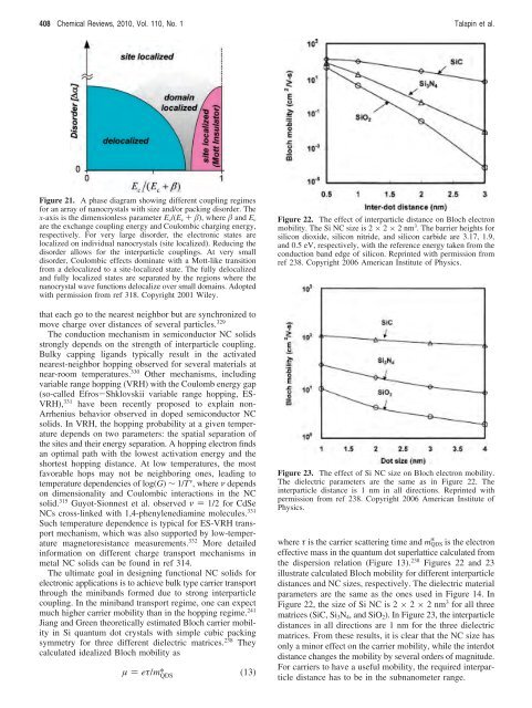
Figure 22. The effect <strong>of</strong> interparticle distance on Bloch electron<br />
mobility. The Si NC size is 2 × 2 × 2nm 3 . The barrier heights <strong>for</strong><br />
silicon dioxide, silicon nitride, and silicon carbide are 3.17, 1.9,<br />
and 0.5 eV, respectively, with the reference energy taken from the<br />
conduction band edge <strong>of</strong> silicon. Reprinted with permission from<br />
ref 238. Copyright 2006 American Institute <strong>of</strong> Physics.<br />
Figure 23. The effect <strong>of</strong> Si NC size on Bloch electron mobility.<br />
The dielectric parameters are the same as in Figure 22. The<br />
interparticle distance is 1 nm in all directions. Reprinted with<br />
permission from ref 238. Copyright 2006 American Institute <strong>of</strong><br />
Physics.<br />
where τ is the carrier scattering time and mQDS * is the electron<br />
effective mass in the quantum dot superlattice calculated from<br />
the dispersion relation (Figure 13). 238 Figures 22 and 23<br />
illustrate calculated Bloch mobility <strong>for</strong> different interparticle<br />
distances and NC sizes, respectively. The dielectric material<br />
parameters are the same as the ones used in Figure 14. In<br />
Figure 22, the size <strong>of</strong> Si NC is 2 × 2 × 2nm3<strong>for</strong> all three<br />
matrices (SiC, Si3N4, and SiO2). In Figure 23, the interparticle<br />
distances in all directions are 1 nm <strong>for</strong> the three dielectric<br />
matrices. From these results, it is clear that the NC size has<br />
only a minor effect on the carrier mobility, while the interdot<br />
distance changes the mobility by several orders <strong>of</strong> magnitude.<br />
For carriers to have a useful mobility, the required interparticle<br />
distance has to be in the subnanometer range.


