

Prospects of Colloidal Nanocrystals for Electronic - Computer Science
Prospects of Colloidal Nanocrystals for Electronic - Computer Science
Prospects of Colloidal Nanocrystals for Electronic - Computer Science

You also want an ePaper? Increase the reach of your titles
YUMPU automatically turns print PDFs into web optimized ePapers that Google loves.
436 Chemical Reviews, 2010, Vol. 110, No. 1 Talapin et al.<br />
I D ) WC i µ sat<br />
2L (V G - V T )2<br />
where µsat is the saturation regime field-effect mobility. This<br />
important parameter is typically calculated from the slope<br />
<strong>of</strong> [ID] 1/2 versus VG.<br />
The charge mobilities extracted from ID-VG curves are<br />
<strong>of</strong>ten higher in the saturated regime than those measured in<br />
the linear regime. This difference in measured carrier<br />
mobility can occur due to contact resistance when a large<br />
part <strong>of</strong> the source-drain voltage drops at the contacts and<br />
not across the channel, due to the presence <strong>of</strong> carrier trapping<br />
centers, etc. 6,557<br />
7.4.2. State-<strong>of</strong>-the-Art <strong>for</strong> Nanocrystal Transistors<br />
(50)<br />
The first inorganic FETs fabricated using colloidal semiconductor<br />
nanoparticles were reported in 1999 by Jacobson<br />
et al. 268 These devices were assembled from pyridine-capped<br />
CdSe NCs. Pyridine is a rather labile and volatile surface<br />
ligand, and annealing <strong>of</strong> the nanoparticle layer above 250<br />
°C allowed sintering <strong>of</strong> CdSe NCs into a polycrystalline<br />
CdSe film. Strictly speaking, the device reported by Jacobson<br />
et al. cannot be assigned to NC FETs because no NCs were<br />
present in the FET channel after annealing above 250 °C. The<br />
device annealed at 350 °C <strong>for</strong> 1 h showed a linear regime<br />
mobility (µlin) <strong>of</strong>1cm 2 /V · s, ION/IOFF ratio <strong>of</strong> 3.1 × 10 4 , and a<br />
threshold voltage <strong>of</strong> 6.7 V. The carrier mobility in those<br />
inorganic FETs was significantly greater than typical mobilities<br />
achieved <strong>for</strong> printed organic FETs. The conductance <strong>of</strong> the NC<br />
films was significantly increased by sintering,; however, the<br />
large concentration <strong>of</strong> structural defects limited the device<br />
switching speeds and induced large hysteresis <strong>of</strong> the ID-VG<br />
scans.<br />
NC-FETs with the conductive channels assembled <strong>of</strong><br />
close-packed quantum confined semiconductor NCs have<br />
been first reported by our team in 2005. 23 As starting material,<br />
we used PbSe NCs capped with oleic acid. Thin NC films<br />
fabricated by spin-coating or drop-casting were very insulating<br />
(σ ≈ 10 -10 Scm -1 ) and did not show any gate effect.<br />
However, replacement <strong>of</strong> bulky oleic acid with small<br />
hydrazine molecules by simply soaking NC films in 1 M<br />
solution <strong>of</strong> N2H4 in acetonitrile reduced the interparticle<br />
spacing from ∼1.2 to ∼0.4 nm and increases conductivity<br />
<strong>of</strong> PbSe NC films by ∼10 orders <strong>of</strong> magnitude. 23 As shown<br />
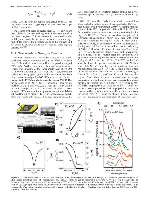
in Figure 52a, the size and shape, as well as the morphology<br />
<strong>of</strong> NC films, did not change after the threatment with<br />
hydrazine solution. Figure 52b shows a current modulation<br />
Ion/I<strong>of</strong>f <strong>of</strong> ∼2.5 × 10 3 <strong>for</strong> a PbSe NC n-FET. In the “on”<br />
state, the low-field specific conductance <strong>of</strong> PbSe NC film<br />
was ∼0.82 S cm -2 , and the current density in saturation<br />
regime approached 2.7 × 10 4 Acm -2 . Field-effect electron<br />
mobilities extracted from a series <strong>of</strong> devices yielded µlin ≈<br />
0.4 cm 2 V -1 s -1 and µsat ≈ 0.7 cm 2 V -1 s -1 in the saturation<br />
regime. Since then, technical improvements is sample<br />
preparation allowed one to achieve respectable electron<br />
mobility approaching µsat ≈ 2.5 cm 2 V -1 s -1 <strong>for</strong> 8 nm PbSe<br />
NC FETs, keeping the Ion/I<strong>of</strong>f ratio above 10 3 . 559 All <strong>of</strong> these<br />
numbers were reported <strong>for</strong> devices prepared at room temperature,<br />
without any heat treatment. Under these conditions,<br />
individual PbSe NCs preserved their QD-type electronic<br />
structure, confirmed by the observation <strong>of</strong> excitonic features<br />
Figure 52. Device characteristis <strong>of</strong> FETs made from ∼8 nm PbSe nanocrystals treated with 1MN2H4 in acetonitrile. (a) SEM images <strong>of</strong> the<br />
FET channel assembled from PbSe nanocrystals. (b) ID and ID 1/2 versus VG curves measured at a constant VDS ) 40 V <strong>for</strong> a n-channel FET, (c)<br />
ID versus VG plot at a constant VDS ) 1 V <strong>for</strong> an ambipolar FET. (d) ID-VDS plot at VDS )-40 V <strong>for</strong> a p-channel FET. Reprinted with permission<br />
from ref 23. Copyright 2005 American Association <strong>for</strong> Advancement <strong>of</strong> <strong>Science</strong>. (e) Extinction spectra <strong>of</strong> PbSe NC films, made from 7.4 nm<br />
nanocrystals, after various chemical treatments. Spectra are vertically <strong>of</strong>fset <strong>for</strong> clarity. Reprinted with permission from ref 560. Copyright 2009<br />
American Chemical Society.


