

Prospects of Colloidal Nanocrystals for Electronic - Computer Science
Prospects of Colloidal Nanocrystals for Electronic - Computer Science
Prospects of Colloidal Nanocrystals for Electronic - Computer Science

You also want an ePaper? Increase the reach of your titles
YUMPU automatically turns print PDFs into web optimized ePapers that Google loves.
416 Chemical Reviews, 2010, Vol. 110, No. 1 Talapin et al.<br />
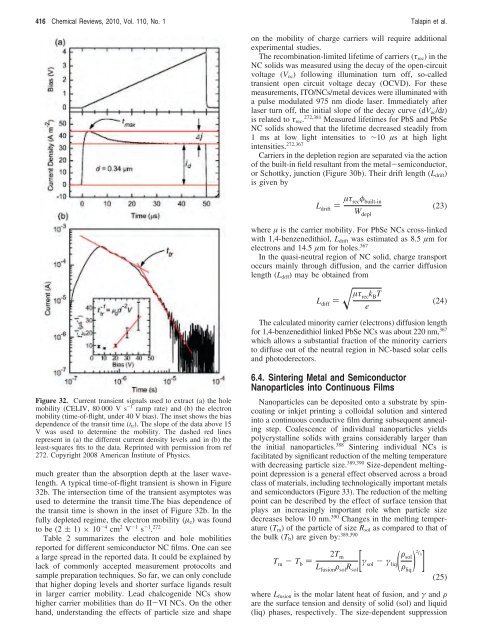
Figure 32. Current transient signals used to extract (a) the hole<br />
mobility (CELIV, 80 000 V s -1 ramp rate) and (b) the electron<br />
mobility (time-<strong>of</strong>-flight, under 40 V bias). The inset shows the bias<br />
dependence <strong>of</strong> the transit time (ttr). The slope <strong>of</strong> the data above 15<br />
V was used to determine the mobility. The dashed red lines<br />
represent in (a) the different current density levels and in (b) the<br />
least-squares fits to the data. Reprinted with permission from ref<br />
272. Copyright 2008 American Institute <strong>of</strong> Physics.<br />
much greater than the absorption depth at the laser wavelength.<br />
A typical time-<strong>of</strong>-flight transient is shown in Figure<br />
32b. The intersection time <strong>of</strong> the transient asymptotes was<br />
used to determine the transit time.The bias dependence <strong>of</strong><br />
the transit time is shown in the inset <strong>of</strong> Figure 32b. In the<br />
fully depleted regime, the electron mobility (µe) was found<br />
to be (2 ( 1) × 10 -4 cm 2 V -1 s -1 . 272<br />
Table 2 summarizes the electron and hole mobilities<br />
reported <strong>for</strong> different semiconductor NC films. One can see<br />
a large spread in the reported data. It could be explained by<br />
lack <strong>of</strong> commonly accepted measurement protocolts and<br />
sample preparation techniques. So far, we can only conclude<br />
that higher doping levels and shorter surface ligands result<br />
in larger carrier mobility. Lead chalcogenide NCs show<br />
higher carrier mobilities than do II-VI NCs. On the other<br />
hand, understanding the effects <strong>of</strong> particle size and shape<br />
on the mobility <strong>of</strong> charge carriers will require additional<br />
experimental studies.<br />
The recombination-limited lifetime <strong>of</strong> carriers (τrec) in the<br />
NC solids was measured using the decay <strong>of</strong> the open-circuit<br />
voltage (Voc) following illumination turn <strong>of</strong>f, so-called<br />
transient open circuit voltage decay (OCVD). For these<br />
measurements, ITO/NCs/metal devices were illuminated with<br />
a pulse modulated 975 nm diode laser. Immediately after<br />
laser turn <strong>of</strong>f, the initial slope <strong>of</strong> the decay curve (dVoc/dt)<br />
is related to τrec. 272,381 Measured lifetimes <strong>for</strong> PbS and PbSe<br />
NC solids showed that the lifetime decreased steadily from<br />
1 ms at low light intensities to ∼10 µs at high light<br />
intensities. 272,367<br />
Carriers in the depletion region are separated via the action<br />
<strong>of</strong> the built-in field resultant from the metal-semiconductor,<br />
or Schottky, junction (Figure 30b). Their drift length (Ldrift)<br />
is given by<br />
L drift ) µτ rec φ built-in<br />
W depl<br />
where µ is the carrier mobility. For PbSe NCs cross-linked<br />
with 1,4-benzenedithiol, Ldrift was estimated as 8.5 µm <strong>for</strong><br />
electrons and 14.5 µm <strong>for</strong> holes. 367<br />
In the quasi-neutral region <strong>of</strong> NC solid, charge transport<br />
occurs mainly through diffusion, and the carrier diffusion<br />
length (Ldiff) may be obtained from<br />
L diff ) � µτ rec k B T<br />
e<br />
The calculated minority carrier (electrons) diffusion length<br />
<strong>for</strong> 1,4-benzenedithiol linked PbSe NCs was about 220 nm, 367<br />
which allows a substantial fraction <strong>of</strong> the minority carriers<br />
to diffuse out <strong>of</strong> the neutral region in NC-based solar cells<br />
and photoderectors.<br />
6.4. Sintering Metal and Semiconductor<br />
Nanoparticles into Continuous Films<br />
(23)<br />
(24)<br />
Nanoparticles can be deposited onto a substrate by spincoating<br />
or inkjet printing a colloidal solution and sintered<br />
into a continuous conductive film during subsequent annealing<br />
step. Coalescence <strong>of</strong> individual nanoparticles yields<br />
polycrystalline solids with grains considerably larger than<br />
the initial nanoparticles. 388 Sintering individual NCs is<br />
facilitated by significant reduction <strong>of</strong> the melting temperature<br />
with decreasing particle size. 389,390 Size-dependent meltingpoint<br />
depression is a general effect observed across a broad<br />
class <strong>of</strong> materials, including technologically important metals<br />
and semiconductors (Figure 33). The reduction <strong>of</strong> the melting<br />
point can be described by the effect <strong>of</strong> surface tension that<br />
plays an increasingly important role when particle size<br />
decreases below 10 nm. 390 Changes in the melting temperature<br />
(Tm) <strong>of</strong> the particle <strong>of</strong> size Rsol as compared to that <strong>of</strong><br />
the bulk (Tb) are given by: 389,390<br />
T m - T b )<br />
2Tm LfusionFsolRsol[ γsol - γliq( F 2<br />
/3<br />
sol<br />
Fliq) where Lfusion is the molar latent heat <strong>of</strong> fusion, and γ and F<br />
are the surface tension and density <strong>of</strong> solid (sol) and liquid<br />
(liq) phases, respectively. The size-dependent suppression<br />
]<br />
(25)


