

Prospects of Colloidal Nanocrystals for Electronic - Computer Science
Prospects of Colloidal Nanocrystals for Electronic - Computer Science
Prospects of Colloidal Nanocrystals for Electronic - Computer Science

Create successful ePaper yourself
Turn your PDF publications into a flip-book with our unique Google optimized e-Paper software.
<strong>Colloidal</strong> <strong>Nanocrystals</strong> in <strong>Electronic</strong> Applications Chemical Reviews, 2010, Vol. 110, No. 1 423<br />
in virtually any semiconductor; however, development <strong>of</strong> a<br />
photoconductor with characteristics suitable <strong>for</strong> a particular<br />
application is a big scientific and technological challenge.<br />
There are several figures <strong>of</strong> merits used to characterize<br />
photoconductive photodetectors. 432,433 These are responsivity,<br />
spectral response, noise-equivalent power (NEP), detectivity,<br />
response time, and frequency response.<br />
Responsivity (Ri). This parameter is also <strong>of</strong>ten called<br />
sensitivity. The responsivity provides a quantitative measure<br />
<strong>for</strong> the output signal such as photocurrent iph per watt <strong>of</strong> the<br />
input optical power Pin. Ri is the function <strong>of</strong> both modulation<br />
frequency (f) and photon wavelength (λ):<br />
R i (f, λ) ) i ph<br />
P in<br />
Spectral response describes the spectral dependence <strong>of</strong> Ri,<br />
that is, the dependence <strong>of</strong> Ri versus λ. Typically, responsivity<br />
<strong>of</strong> IR detectors rises monotonically with increasing wavelength,<br />
then peaks and drops to zero upon reaching semiconductor<br />
band gap energy (so-called cut<strong>of</strong>f wavelength <strong>of</strong><br />
intrinsic photodetector). In NC photodetectors, the spectral<br />
response generally follows the shape <strong>of</strong> the NC absorption<br />
spectrum.<br />
Noise-Equivalent-Power. The internal noise current in is<br />
the main factor limiting the ability to detect small optical<br />
signals because the signal produced by the input power must<br />
be above the noise level. The noise-equivalent-power (NEP)<br />
is determined as a light power that yields a signal-to-noise<br />
ratio equal to 1 and can be expressed as:<br />
NEP ) i n<br />
R i<br />
Detectivity. For comparison <strong>of</strong> different devices, it is<br />
important to provide an area independent figure <strong>of</strong> merit D*<br />
(detectivity):<br />
D*(λ, f) ) R i √A∆f<br />
i n<br />
where A is the detector area. The detectivity D* is the rootmean-square<br />
signal-to-noise output when 1 W <strong>of</strong> monochromatic<br />
radiant flux modulated at frequency f is incident on 1<br />
cm 2 detector area, with a noise-equivalent bandwidth <strong>of</strong> 1<br />
Hz. D* is typically reported in Jones (1 Jones ) 1cmHz 1/2<br />
W -1 ).<br />
Response time (t). Response time, also known as the time<br />
constant, is calculated as follows:<br />
t ) 1<br />
2πf 3db<br />
(32)<br />
(33)<br />
where f3db is the frequency at which the signal power is 3<br />
dB lower than the value at zero frequency; that is, the<br />
photocurrent is 1/�2 ≈ 0.707 <strong>of</strong> that at zero frequency.<br />
Frequency Response. At low modulation frequencies, the<br />
photocurrent can follow the rise/decay <strong>of</strong> the illumination<br />
intensity. However, at higher frequencies, responsivity<br />
becomes a strong function <strong>of</strong> the response time:<br />
R 0<br />
R(f) )<br />
√1 + (2πft) 2<br />
(34)<br />
(35)<br />
(36)<br />
where R0 is the responsivity at zero frequency, and t is the<br />
response time.<br />
Other important characteristics <strong>of</strong> photodetectors are the<br />
linear dynamic range (the range over which detector responds<br />
linearly to the incident optical power) and the noise spectrum<br />
(i.e., the dependence <strong>of</strong> in vs f).<br />
7.2.2. Photoconductivity in Nanocrystal Solids<br />
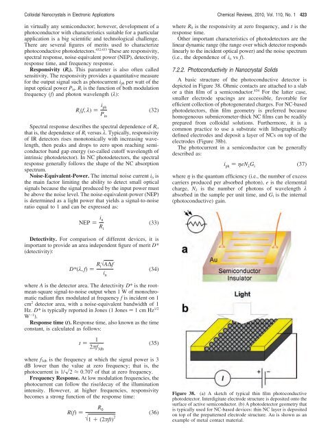
A basic structure <strong>of</strong> the photoconductive detector is<br />
depicted in Figure 38. Ohmic contacts are attached to a slab<br />
or a thin film <strong>of</strong> a semiconductor. 434 For the latter case,<br />
smaller electrode spacings are accessible, favorable <strong>for</strong><br />
efficient collection <strong>of</strong> photogenerated charges. For NC-based<br />
photodetectors, thin film geometry is preferred because<br />
homogeneous submicrometer-thick NC films can be readily<br />
prepared from colloidal solutions. Furthermore, it is a<br />
common practice to use a substrate with lithographically<br />
defined electrodes and deposit a layer <strong>of</strong> NCs on top <strong>of</strong> the<br />
electrodes (Figure 38b).<br />
The photocurrent in a semiconductor can be generally<br />
described as:<br />
i ph ) ηeN λ G i<br />
(37)<br />
where η is the quantum efficiency (i.e., the number <strong>of</strong> excess<br />
carriers produced per absorbed photon), e is the elemental<br />
charge, Nλ is the number <strong>of</strong> photons <strong>of</strong> wavelength λ<br />
absorbed in the sample per unit time, and Gi is the internal<br />
(photoconductive) gain.<br />
Figure 38. (a) A sketch <strong>of</strong> typical thin film photoconductive<br />
photodetector. Interdigitate electrode structure is deposited onto the<br />
surface <strong>of</strong> active semiconductor. (b) A photodetector geometry that<br />
is typically used <strong>for</strong> NC-based devices: thin NC layer is deposited<br />
on top <strong>of</strong> the prepatterned electrode structure. Au is shown as an<br />
example <strong>of</strong> metal contact material.


