

Prospects of Colloidal Nanocrystals for Electronic - Computer Science
Prospects of Colloidal Nanocrystals for Electronic - Computer Science
Prospects of Colloidal Nanocrystals for Electronic - Computer Science

You also want an ePaper? Increase the reach of your titles
YUMPU automatically turns print PDFs into web optimized ePapers that Google loves.
<strong>Colloidal</strong> <strong>Nanocrystals</strong> in <strong>Electronic</strong> Applications Chemical Reviews, 2010, Vol. 110, No. 1 447<br />
Si NCs embedded into Ge matrix. 666 Humphrey and Linke<br />
derived conditions under which reversible diffusive electron<br />
transport could be achieved in nanostructured thermoelectric<br />
materials. 667 Their work further supported the idea that deltafunctional<br />
density <strong>of</strong> states is optimal <strong>for</strong> thermoelectric<br />
materials and predicted that optimized nanostructured materials<br />
with a delta-like DOS may have ZT approaching 10 at<br />
room temperature. This exciting prediction originated from<br />
the fundamental difference between thermodynamics and<br />
transport in nanostructured materials as compared to bulk<br />
semiconductors. 667 In 2008, Mueller reported an encouraging<br />
theoretical study <strong>of</strong> TE behavior in an array <strong>of</strong> molecular<br />
junctions. 659<br />
The experimental studies <strong>of</strong> low-dimensional TE materials<br />
supported optimistic theoretical predictions. Harman et al.<br />
observed ZT ≈ 1.6 in a PbSeTe-based quantum dot superlattice<br />
grown by molecular beam epitaxy (MBE), 12 Venkatasubramanian<br />
et al. achieved ZT ≈ 2.4 in a p-type Bi2Te3/<br />
Sb2Te3 superlattice, 668 and Hsu et al. reported ZT ≈ 2.2 in<br />
alloys containing nanometer-sized metallic grains embedded<br />
in a semiconducting matrix. 669 In 2008, Heath et al. 670 and<br />
Yang et al. 671 reported very high ZT values measured <strong>for</strong><br />
individual Si nanowires. Most <strong>of</strong> these ZT enhancements<br />
were attributed to lowering the thermal conductance due to<br />
phonon scattering at the heterointerfaces and grain boundaries.<br />
However, until very recently, practical use <strong>of</strong> these<br />
materials was hampered by complicated and expensive<br />
synthesis techniques, such as molecular beam epitaxy. 12 In<br />
the last several years, important steps toward cost-effective<br />
nanostructured TE materials were reported. The Kanatzidis<br />
group synthesized several families <strong>of</strong> complex chalcogenide<br />
phases, such as n-type AgPb18+xSbTe20 (LAST) 669 and p-type<br />
Na0.95Pb20SbTe22 (SALT) 672 showing ZT values <strong>of</strong> ∼1.7 and<br />
1.6, respectively. These high ZT values originated from low<br />
thermal conductivity caused by the presence <strong>of</strong> nanoscale<br />
inclusions in the host material spontaneously <strong>for</strong>med due to<br />
phase separation during crystallization <strong>of</strong> melted phase. In<br />
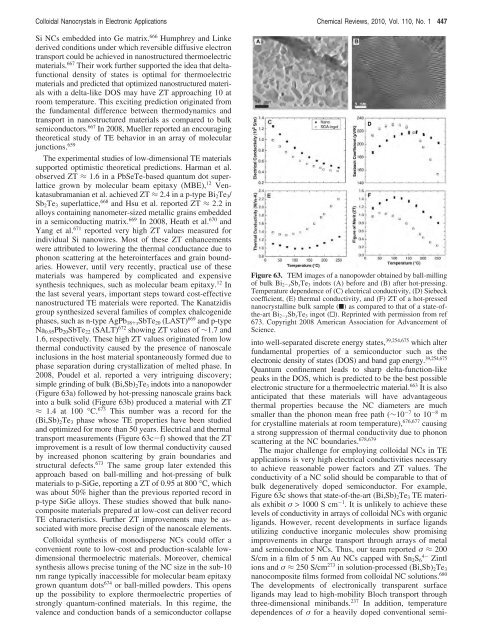
2008, Poudel et al. reported a very intriguing discovery;<br />
simple grinding <strong>of</strong> bulk (Bi,Sb)2Te3 indots into a nanopowder<br />
(Figure 63a) followed by hot-pressing nanoscale grains back<br />
into a bulk solid (Figure 63b) produced a material with ZT<br />
≈ 1.4 at 100 °C. 673 This number was a record <strong>for</strong> the<br />
(Bi,Sb)2Te3 phase whose TE properties have been studied<br />
and optimized <strong>for</strong> more than 50 years. Electrical and thermal<br />
transport measurements (Figure 63c-f) showed that the ZT<br />
improvement is a result <strong>of</strong> low thermal conductivity caused<br />
by increased phonon scattering by grain boundaries and<br />
structural defects. 673 The same group later extended this<br />
approach based on ball-milling and hot-pressing <strong>of</strong> bulk<br />
materials to p-SiGe, reporting a ZT <strong>of</strong> 0.95 at 800 °C, which<br />
was about 50% higher than the previous reported record in<br />
p-type SiGe alloys. These studies showed that bulk nanocomposite<br />
materials prepared at low-cost can deliver record<br />
TE characteristics. Further ZT improvements may be associated<br />
with more precise design <strong>of</strong> the nanoscale elements.<br />
<strong>Colloidal</strong> synthesis <strong>of</strong> monodisperse NCs could <strong>of</strong>fer a<br />
convenient route to low-cost and production-scalable lowdimensional<br />
thermoelectric materials. Moreover, chemical<br />
synthesis allows precise tuning <strong>of</strong> the NC size in the sub-10<br />
nm range typically inaccessible <strong>for</strong> molecular beam epitaxy<br />
grown quantum dots 674 or ball-milled powders. This opens<br />
up the possibility to explore thermoelectric properties <strong>of</strong><br />
strongly quantum-confined materials. In this regime, the<br />
valence and conduction bands <strong>of</strong> a semiconductor collapse<br />
into well-separated discrete energy states, 39,254,675 which alter<br />
fundamental properties <strong>of</strong> a semiconductor such as the<br />
electronic density <strong>of</strong> states (DOS) and band gap energy. 39,254,675<br />
Quantum confinement leads to sharp delta-function-like<br />
peaks in the DOS, which is predicted to be the best possible<br />
electronic structure <strong>for</strong> a thermoelectric material. 663 It is also<br />
anticipated that these materials will have advantageous<br />
thermal properties because the NC diameters are much<br />
smaller than the phonon mean free path (∼10-7 to 10-8 m<br />
<strong>for</strong> crystalline materials at room temperature), 676,677 causing<br />
a strong suppression <strong>of</strong> thermal conductivity due to phonon<br />
scattering at the NC boundaries. 678,679<br />
The major challenge <strong>for</strong> employing colloidal NCs in TE<br />
applications is very high electrical conductivities necessary<br />
to achieve reasonable power factors and ZT values. The<br />
conductivity <strong>of</strong> a NC solid should be comparable to that <strong>of</strong><br />
bulk degeneratively doped semiconductor. For example,<br />
Figure 63c shows that state-<strong>of</strong>-the-art (Bi,Sb)2Te3 TE materials<br />
exhibit σ > 1000 S cm-1 . It is unlikely to achieve these<br />
levels <strong>of</strong> conductivity in arrays <strong>of</strong> colloidal NCs with organic<br />
ligands. However, recent developments in surface ligands<br />
utilizing conductive inorganic molecules show promising<br />
improvements in charge transport through arrays <strong>of</strong> metal<br />
and semiconductor NCs. Thus, our team reported σ ≈ 200<br />
S/cm in a film <strong>of</strong> 5 nm Au NCs capped with Sn2S6 4- Zintl<br />
ions and σ ≈ 250 S/cm273 in solution-processed (Bi,Sb)2Te3<br />
nanocomposite films <strong>for</strong>med from colloidal NC solutions. 680<br />
The developments <strong>of</strong> electronically transparent surface<br />
ligands may lead to high-mobility Bloch transport through<br />
three-dimensional minibands. 237 Figure 63. TEM images <strong>of</strong> a nanopowder obtained by ball-milling<br />
<strong>of</strong> bulk Bi2-xSbxTe3 indots (A) be<strong>for</strong>e and (B) after hot-pressing.<br />
Temperature dependence <strong>of</strong> (C) electrical conductivity, (D) Siebeck<br />
coefficient, (E) thermal conductivity, and (F) ZT <strong>of</strong> a hot-pressed<br />
nanocrystalline bulk sample (9) as compared to that <strong>of</strong> a state-<strong>of</strong>the-art<br />
Bi2-xSbxTe3 ingot (0). Reprinted with permission from ref<br />
673. Copyright 2008 American Association <strong>for</strong> Advancement <strong>of</strong><br />
<strong>Science</strong>.<br />
In addition, temperature<br />
dependences <strong>of</strong> σ <strong>for</strong> a heavily doped conventional semi-


