Prospects of Colloidal Nanocrystals for Electronic - Computer Science
Prospects of Colloidal Nanocrystals for Electronic - Computer Science
Prospects of Colloidal Nanocrystals for Electronic - Computer Science
Create successful ePaper yourself
Turn your PDF publications into a flip-book with our unique Google optimized e-Paper software.
390 Chemical Reviews, 2010, Vol. 110, No. 1 Talapin et al.<br />
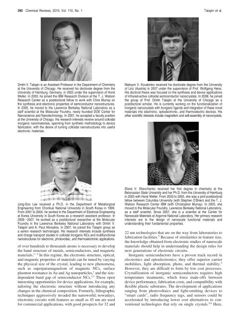
Dmitri V. Talapin is an Assistant Pr<strong>of</strong>essor in the Department <strong>of</strong> Chemistry<br />
at the University <strong>of</strong> Chicago. He received his doctorate degree from the<br />
University <strong>of</strong> Hamburg, Germany, in 2002 under the supervision <strong>of</strong> Horst<br />
Weller. In 2003, he joined the IBM Research Division at the T. J. Watson<br />
Research Center as a postdoctoral fellow to work with Chris Murray on<br />
the synthesis and electronic properties <strong>of</strong> semiconductor nanostructures.<br />
In 2005, he moved to the Lawrence Berkeley National Laboratory as a<br />
staff scientist at the Molecular Foundry, newly founded DOE Center <strong>for</strong><br />
Nanoscience and Nanotechnology. In 2007, he accepted a faculty position<br />
at the University <strong>of</strong> Chicago. His research interests revolve around colloidal<br />
inorganic nanomaterials, spanning from synthetic methodology to device<br />
fabrication, with the desire <strong>of</strong> turning colloidal nanostructures into useful<br />
electronic materials.<br />
Jong-Soo Lee received a Ph.D. in the Department <strong>of</strong> Metallurgical<br />
Engineering from Chonbuk National University in South Korea in 1999.<br />
From 2001 to 2004, he worked in the Department <strong>of</strong> Electrical Engineering<br />
at Korea University in South Korea as a research assistant pr<strong>of</strong>essor. In<br />
2006-2007, he worked as a postdoctoral researcher at the Molecular<br />
Foundry in the Lawrence Berkeley National Laboratory with Dmitri V.<br />
Talapin and A. Paul Alivisatos. In 2007, he joined the Talapin group as<br />
a senior research technologist. His research interests include synthesis<br />
and charge transport studies in colloidal inorganic NCs and multifunctional<br />
nanostructures <strong>for</strong> electronic, photovoltaic, and thermoelectronic applications.<br />
<strong>of</strong> over hundreds to thousands atoms is necessary to develop<br />
the band structure <strong>of</strong> metals, semiconductors, and magnetic<br />
materials. 1-4 In this regime, the electronic structure, optical,<br />
and magnetic properties <strong>of</strong> materials can be tuned by varying<br />
the physical size <strong>of</strong> the crystal, leading to new phenomena,<br />
such as superparamagnetism <strong>of</strong> magnetic NCs, surface<br />
plasmon resonance in Au and Ag nanoparticles, 1 and the sizedependent<br />
band gap <strong>of</strong> semiconductor NCs. 2,3 These open<br />
interesting opportunities <strong>for</strong> device applications, <strong>for</strong> example,<br />
tailoring the electronic structure without introducing any<br />
changes in the chemical composition. Formerly, lithographic<br />
techniques aggressively invaded the nanoworld; nowadays,<br />
electronic circuits with features as small as 45 nm are used<br />
<strong>for</strong> commercial applications, with good prospects <strong>for</strong> 32 and<br />
Maksym V. Kovalenko received his doctorate degree from the University<br />
<strong>of</strong> Linz (Austria) in 2007 under the supervision <strong>of</strong> Pr<strong>of</strong>. Wolfgang Heiss.<br />
His doctoral thesis was focused on the synthesis and device applications<br />
<strong>of</strong> infrared-active colloidal semiconductor nanocrystals. In 2008, he joined<br />
the group <strong>of</strong> Pr<strong>of</strong>. Dmitri Talapin at the University <strong>of</strong> Chicago as a<br />
postdoctoral scholar. He is currently working on the functionalization <strong>of</strong><br />
inorganic nanocrystals with inorganic ligands and integration <strong>of</strong> these novel<br />
materials into electronic, optoelectronic, and thermoelectric devices. His<br />
other scientific interests include magnetism and self-assembly <strong>of</strong> nanocrystals.<br />
Elena V. Shevchenko received her first degree in chemistry at the<br />
Belorussian State University and her Ph.D. from the University <strong>of</strong> Hamburg<br />
in 2003 with Horst Weller. From 2003 to 2005, she was a joint postdoctoral<br />
fellow between Columbia University (with Stephen O’Brien) and the T. J.<br />
Watson Research Center IBM (with Christopher Murray). In 2005, she<br />
moved to the Molecular Foundry, Lawrence Berkeley National Laboratory,<br />
as a staff scientist. Since 2007, she is a scientist at the Center <strong>for</strong><br />
Nanoscale Materials at Argonne National Laboratory. Her primary research<br />
interests are in the design <strong>of</strong> nanoscale functional materials and<br />
understanding their fundamental properties.<br />
22 nm technologies that are on the way from laboratories to<br />
fabrication facilities. 5 Because <strong>of</strong> similarities in feature size,<br />
the knowledge obtained from electronic studies <strong>of</strong> nanoscale<br />
materials should help in understanding the design rules <strong>for</strong><br />
next generations <strong>of</strong> electronic circuits.<br />
Inorganic semiconductors have a proven track record in<br />
electronics and optoelectronics; they <strong>of</strong>fer superior carrier<br />
mobilities, light absorption, photo, and thermal stability. 5<br />
However, they are difficult to <strong>for</strong>m by low cost processes.<br />
Crystallization <strong>of</strong> inorganic semiconductors requires high<br />
temperature treatments, which <strong>for</strong>ce trade-<strong>of</strong>fs between<br />
device per<strong>for</strong>mance, fabrication costs, and compatibility with<br />
flexible plastic substrates. The development <strong>of</strong> applications<br />
ranging from photovoltaics and light-emitting devices to<br />
“smart cards”, radio frequency tags, and sensors could be<br />
accelerated by introducing lower cost alternatives to conventional<br />
technologies that rely on single crystals. 5,6 Here,


