

Prospects of Colloidal Nanocrystals for Electronic - Computer Science
Prospects of Colloidal Nanocrystals for Electronic - Computer Science
Prospects of Colloidal Nanocrystals for Electronic - Computer Science

Create successful ePaper yourself
Turn your PDF publications into a flip-book with our unique Google optimized e-Paper software.
<strong>Colloidal</strong> <strong>Nanocrystals</strong> in <strong>Electronic</strong> Applications Chemical Reviews, 2010, Vol. 110, No. 1 407<br />
Figure 18. Low-temperature resistance (R) <strong>of</strong> a layer <strong>of</strong> 5 nm Au<br />
NCs linked by HS(CH2)nSH molecules with various n. The<br />
resistances are normalized to their respective values at 200 K. Inset:<br />
R <strong>of</strong> the samples at 200 K as a function <strong>of</strong> n. Reprinted with<br />
permission from ref 260. Copyright 2006 American Institute <strong>of</strong><br />
Physics.<br />
19b-d). Correspondingly, the electrical conductivity increased<br />
by ∼11 orders <strong>of</strong> magnitude, and the material<br />
converted from highly insulating (Figure 19e) to metallic273 (Figure 19f). In the case <strong>of</strong> CdSe NCs capped by Sn2S6 4-<br />
Figure 19. Conductivity <strong>of</strong> 5 nm Au nanocrystals stabilized by<br />
Sn2S6<br />
ions, the delocalization <strong>of</strong> electron and hole wave functions<br />
manifested itself through the red shift <strong>of</strong> excitonic transitions<br />
in the optical absorption spectra.<br />
4- . (A) Sketch <strong>of</strong> Au nanocrystal capped with Sn2S6 4- ions.<br />
(B) TEM image <strong>of</strong> Au nanocrystals capped with dodecanethiol.<br />
(C,D) TEM images <strong>of</strong> 2D and 3D superlattices <strong>for</strong>med by Au<br />
nanocrystals capped with Sn2S6 4- . (E) I-V scan <strong>for</strong> ∼200 nm thick<br />
film <strong>of</strong> dodecanethiol-capped Au nanocrystals. (F) I-V scan <strong>for</strong><br />
∼200 nm thick films <strong>of</strong> Au nanocrystals stabilized with Sn2S6 4- .<br />
Adapted with permission from ref 273. Copyright 2009 American<br />
Association <strong>for</strong> Advancement <strong>of</strong> <strong>Science</strong>.<br />
5.3. Effects <strong>of</strong> <strong>Electronic</strong> and Structural Disorder<br />
Disorder (∆R) is the other key player in the electronic<br />
properties <strong>of</strong> NC solids. Because the NCs are not atomically<br />
defined objects, there is always a finite dispersion in their<br />
size and shape. Advanced synthetic techniques allow <strong>for</strong><br />
dispersion within a single atomic layer, 30,326 which still leads<br />
to a standard deviation <strong>of</strong> several percent. Size distribution<br />
results in the finite dispersion <strong>of</strong> the orbital energies (R) <strong>of</strong><br />
individual particles. The energies <strong>of</strong> occupied and unoccupied<br />
states in semiconductor quantum dots, scale approximately<br />
as 1/r2 , 318,319 leading to ∆R/R ≈ 2∆r/r dispersion in site<br />
energies due to quantum confinement. Electron transfer<br />
between two NCs is the most efficient when their energies<br />
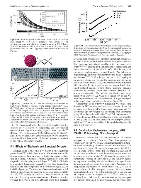
Figure 20. The temperature dependence <strong>of</strong> the experimentally<br />
determined low-bias resistance <strong>for</strong> 7 nm Ag nanoparticle monolayer<br />
films with different amount <strong>of</strong> disorder originating from the particle<br />
size distribution. Reprinted with permission from ref 328. Copyright<br />
2002 American Association <strong>for</strong> Advancement <strong>of</strong> <strong>Science</strong>.<br />
are equal (the conditions <strong>of</strong> resonant tunneling); otherwise,<br />
phonons have to be absorbed or emitted during the transition.<br />
The transition rate drops quickly with increasing disorder,<br />
320,327,328 pointing to the importance <strong>of</strong> narrow size and<br />
shape distribution <strong>of</strong> individual NCs. The interplay <strong>of</strong><br />
exchange coupling energy � and disorder ∆R defines an<br />
important type <strong>of</strong> metal-insulator transition called Anderson<br />
localization. 315,319 If � is larger than ∆R, the coupling is<br />
sufficiently strong to overcome the dispersion in the energy<br />
levels <strong>of</strong> the individual NCs, and extended wave functions<br />
still can exist. In the opposite case, the system breaks into<br />
small isolated regions where strong coupling prevails,<br />
separated by weakly conducting regions. Heath et al.<br />
observed a dramatic effect <strong>of</strong> size distribution on charge<br />
transport in arrays <strong>of</strong> Ag NCs; the conductivity <strong>of</strong> the NC<br />
monolayers changed over several orders <strong>of</strong> magnitude upon<br />
rather small change <strong>of</strong> ∆R as shown in Figure 20.<br />
Another type <strong>of</strong> disorder very typical <strong>for</strong> NC solids is the<br />
disorder in NC packing that leads to variation <strong>of</strong> spacing<br />
between neighboring NCs. Here, long-range ordered NC<br />
assemblies can have significant advantage over disordered<br />
glassy films. Remacle and Levine 318 and Beloborodov et al. 314<br />
presented a detailed theoretical framework <strong>for</strong> the interplay<br />
<strong>of</strong> ∆R, �, and Ec and their effect on the transport characteristics<br />
<strong>of</strong> NC solids; an outline <strong>of</strong> the trends is schematically<br />
shown in Figure 21.<br />
5.4. Conduction Mechanisms: Hopping, VRH,<br />
ES-VRH, Cotunneling, Bloch Transport<br />
Important in<strong>for</strong>mation on the mechanism <strong>of</strong> charge<br />
transport can be obtained from the effect <strong>of</strong> temperature on<br />
conductivity (G) <strong>of</strong> NC solids. Typical temperature dependences<br />
<strong>for</strong> conductivity <strong>of</strong> monolayer thick films <strong>of</strong> metal NCs<br />
are shown in Figure 20. At high temperatures (>200 K),<br />
close-packed layers <strong>of</strong> monodisperse metal NC can exhibit<br />
an increase in resistance with increasing temperature, the<br />
behavior typical <strong>for</strong> metals. 328 At lower temperatures, the<br />
carriers are localized on individual NCs and transport occurs<br />
by sequential tunneling; the electron hops from a particle to<br />
its nearest neighbor along the current path. Arrhenius type<br />
temperature dependence <strong>of</strong> conductivity log(G) ∼ 1/T is<br />
characteristic <strong>of</strong> this transport regime. At even lower<br />
temperatures, below ∼60 K the conductivity <strong>of</strong> Au and Ag<br />
NC layers scales as log(G) ∼ 1/T 1/2 . 328,329 Tran et al.<br />
explained such behavior by inelastic cotunneling transport<br />
mechanism dominated by cooperative, multielectron hops


