

Prospects of Colloidal Nanocrystals for Electronic - Computer Science
Prospects of Colloidal Nanocrystals for Electronic - Computer Science
Prospects of Colloidal Nanocrystals for Electronic - Computer Science

You also want an ePaper? Increase the reach of your titles
YUMPU automatically turns print PDFs into web optimized ePapers that Google loves.
<strong>Colloidal</strong> <strong>Nanocrystals</strong> in <strong>Electronic</strong> Applications Chemical Reviews, 2010, Vol. 110, No. 1 395<br />
Formation <strong>of</strong> hollow Au NCs allowed one to engineer their<br />
optical properties because the frequency <strong>of</strong> surface plasmon<br />
resonance in a hollow NC was strongly dependent on the<br />
shell thickness and shape. 153<br />
2.3. Multicomponent <strong>Colloidal</strong> Nanostructures<br />
One <strong>of</strong> the most exciting aspects <strong>of</strong> colloidally synthesized<br />
nanomaterials is the possibility to prepare various multicomponent<br />
nanostructures. Combining materials at the nanoscale<br />
opens up additional opportunities <strong>for</strong> manipulating<br />
wave functions, Plasmon resonances, spins, and other materials<br />
properties. 36,37,154 Thus, bringing together components <strong>of</strong><br />
intrinsically different functionality constitutes a particularly<br />
powerful route to creating novel functional materials with<br />
synergetic properties found in neither <strong>of</strong> the constituents.<br />
Multicomponent nanostructures can be prepared via multistep<br />
syntheses where presynthesized NCs are used as seeds <strong>for</strong><br />
nucleation and growth <strong>of</strong> other inorganic phase. Significant<br />
progress has been achieved in the synthesis <strong>of</strong> core-shell<br />
NCs combining two different semiconductors, 49,94,155-157<br />
metals, 158,159 or a metal and a semiconductor160 in the <strong>for</strong>m<br />
<strong>of</strong> a concentric core and shell (Figure 5a). Such morphology<br />
can be obtained by growing a uni<strong>for</strong>m layer <strong>of</strong> a shell<br />
material around colloidal particles. In the case <strong>of</strong> epitaxial<br />
semiconductor-semiconductor core-shell NCs, the choice<br />
<strong>of</strong> materials <strong>for</strong> the core and the shell allows <strong>for</strong> controlling<br />
the confinement <strong>of</strong> electron and hole wave functions, which,<br />
in turn, determines their optical and electronic properties. If<br />
a narrow gap semiconductor is covered by a shell <strong>of</strong> semiconductor<br />
with wide band gap, both electron and hole wave<br />
functions will be strongly confined to the core (Figure 5b,<br />
left). This confinement regime called type-I heterostructure<br />
is observed, <strong>for</strong> example, in CdSe/ZnS, 49,155 InAs/ZnSe, 161,162<br />
InP/ZnS, 163 and other systems. It is favorable <strong>for</strong> achieving<br />
high quantum efficiency and stability <strong>of</strong> photo- and elec-<br />
Figure 5. (a) Structure <strong>of</strong> a core-shell nanocrystal optimized <strong>for</strong><br />
high luminescence efficiency and stability. Reproduced with<br />
permission from ref 171. (b) Schematic representation <strong>of</strong> the band<br />
structure <strong>of</strong> (left) CdSe/ZnS, (middle) CdSe/CdS, and (right) CdTe/<br />
CdSe core shell nanocrystals. The radial probability functions <strong>for</strong><br />
the lowest energy electron and hole wave functions are schematically<br />
shown as red and blue curves, respectively. (c) An example<br />
<strong>of</strong> a nanostructure where electron and hole have different confinement<br />
regimes: the electron and hole are confined in two and three<br />
dimensions, respectively.<br />
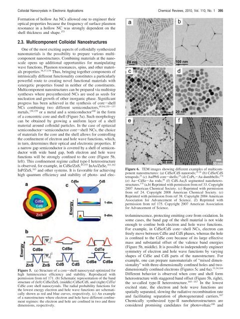
Figure 6. TEM images showing different examples <strong>of</strong> multicomponent<br />
nanostructures: (a) CdSe/CdS nanorods; 33,34 (b) CdSe/CdS<br />
tetrapods; 33 (c) Au/PbS core-shells; 24 (d) CoPt3-Au dumbbells; 174<br />
(e) Au-CdSe-Au rods; 38 (f) CdS-Au2S segmented nanoheterostructures.<br />
175 (a,b) Reprinted with permission from ref 33. Copyright<br />
2007 American Chemical Society. (c) Reprinted with permission<br />
from ref 24. Copyright 2008 American Chemical Society. (e)<br />
Reprinted with permission from ref 38. Copyright 2004 American<br />
Association <strong>for</strong> Advancement <strong>of</strong> <strong>Science</strong>. (f) Reprinted with<br />
permission from ref 175. Copyright 2007 American Association<br />
<strong>for</strong> Advancement <strong>of</strong> <strong>Science</strong>.<br />
troluminescence, protecting emitting core from oxidation. In<br />
some cases, the band gap <strong>of</strong> the shell material is not wide<br />
enough to confine both electron and hole wave functions.<br />
For example, in CdSe/CdS core-shell NCs, electron can<br />
freely move between CdSe and CdS phases, whereas the hole<br />
is confined to the CdSe core because <strong>of</strong> its large effective<br />
mass and substantial <strong>of</strong>fset <strong>of</strong> the valence band energies<br />
(Figure 5b, middle). It is possible to independently engineer<br />
symmetry <strong>of</strong> electron and hole wave functions by varying<br />
shapes <strong>of</strong> CdSe and CdS parts <strong>of</strong> the nanostructure. For<br />
example, one can prepare nanomaterials <strong>of</strong> “mixed dimensionality”<br />
with three-dimensionally confined holes and twodimensionally<br />
confined electrons (Figures 5c and 6a). 33,34,164<br />
Different behavior is observed when core and shell <strong>for</strong>m<br />
heterostructure with staggered band <strong>of</strong>fset (Figure 5b, right),<br />
the so-called type-II heterostructure. 165-167 In the lowest<br />
excited state, the electron and hole wave functions are<br />
spatially separated, slowing the radiative recombination rate<br />
and facilitating separation <strong>of</strong> photogenerated carriers. 167<br />
Chemically synthesized type-II nanoheterostructures are<br />
considered promising candidates <strong>for</strong> photovoltaic 168 and


