

Prospects of Colloidal Nanocrystals for Electronic - Computer Science
Prospects of Colloidal Nanocrystals for Electronic - Computer Science
Prospects of Colloidal Nanocrystals for Electronic - Computer Science

Create successful ePaper yourself
Turn your PDF publications into a flip-book with our unique Google optimized e-Paper software.
414 Chemical Reviews, 2010, Vol. 110, No. 1 Talapin et al.<br />
ductors, when there is no appropriate metal available to <strong>for</strong>m<br />
a low-barrier contact, a tunnel contact is used. Such contacts<br />
do have a positive barrier at the metal-semiconductor<br />
interface, but also have a high enough doping in the<br />
semiconductor that there is only a thin potential barrier<br />
separating the metal from the semiconductor. If the width<br />
<strong>of</strong> the depletion region at the metal-semiconductor interface<br />
is very thin, carriers can readily tunnel across such barrier.<br />
Gyout-Sionnest demonstrated that doping <strong>of</strong> CdSe NCs by<br />
potassium evaporation or by electrochemical charging results<br />
in the <strong>for</strong>mation <strong>of</strong> ohmic electron-injecting contacts with<br />
Au and even Pt (� ≈ 5.6 eV) electrodes. 185<br />
Often, the interface exhibits an additional dipole barrier<br />
that tends to change the metal work function 368,369 and hence<br />
the interface barrier height. Intentionally introduced dipoles<br />
at the metal surface, <strong>for</strong> example, through self-assembled<br />
monolayers (SAMs), were used to improve charge injection<br />
into organic semiconductors, as demonstrated by de Boer et<br />
al. 370 and Hamadani et al. 371 The I-V characteristic should<br />
also depend on the density <strong>of</strong> electronic states in contacts<br />
and NC solids. The electronic structure <strong>of</strong> NC solids with<br />
sharp spikes in the density <strong>of</strong> states can lead to unusual<br />
electronic properties. Thus, the Heath group reported tunnel<br />
diode behavior with pronounced negative differential resistance<br />
<strong>for</strong> Au/SAM/CdSe_NCs/SAM/Au structure. 372<br />
Contact resistance can be measured as the voltage drop at<br />
the electrodes with noncontact scanning probe potentiometry<br />
(e.g., Kelvin probe), 373 by four-point probe measurements, 374<br />
or by determining the channel resistance <strong>of</strong> transitors with<br />
different channel lengths and extrapolating to zero channel<br />
length (transfer line method). 375,376 There is only limited<br />
experimental in<strong>for</strong>mation available <strong>for</strong> the contact resistance<br />
at the metal-NC interface. At the same time, some useful<br />
analogies can be drawn between metal-NC interface discussed<br />
here and much better studied metal-bulk semiconductor<br />
and metal–organic semiconductor interfaces. We<br />
would like to address the readers to several reviews describing<br />
charge injectrion and associated effects in inorganic 377 and<br />
organic 376,378,379 semiconductors.<br />
6.2. Schottky Barriers to Nanocrystal Solids<br />
Sargent and Nozik groups recently reported that vacuum<br />
deposition <strong>of</strong> low work function metal electrodes (Ca, Mg,<br />
Al) on a film <strong>of</strong> lead chalcogenide (PbS or PbSe) NCs leads<br />
to the <strong>for</strong>mation <strong>of</strong> a Schottky barrier at the interface between<br />
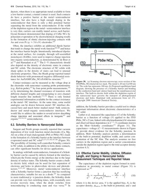
evaporated metal and NC solid 22,271,272,366,367,380 (Figure 30).<br />
The possibility <strong>of</strong> <strong>for</strong>ming well-controlled Schottky contacts<br />
to NC solids, in addition to the ability to <strong>for</strong>m ohmic contacts,<br />
can <strong>of</strong>fer significant benefits <strong>for</strong> device applications.<br />
In analogy with bulk semiconductors, <strong>for</strong>mation <strong>of</strong> a Schottky<br />
barrier can be caused by defects <strong>for</strong>med at the interface,<br />
which pin the Fermi energy at the interface due to the large<br />
density <strong>of</strong> surface states. The Schottky barrier creates a builtin<br />
electric field, which can be used <strong>for</strong> fast separation <strong>of</strong><br />
electrons and holes in photovoltaic devices and photodetectors.<br />
22,271,367 Moreover, metal-semiconductor interface<br />
with a Schottky barrier <strong>for</strong>ms a junction that has rectifying<br />
characteristics, suitable <strong>for</strong> use as a diode. 365 As compared<br />
to more traditional p-n junction diodes, the Schottky diode<br />
can provide very fast switching times, with essentially zero<br />
reverse recovery time, when the diode switches from<br />
nonconducting to conducting state and vice versa. 381 In<br />
Figure 30. (a) Scanning electron microscopy cross-section <strong>of</strong> the<br />
ITO/PbSe_NCs/metal device stack. The metal is 20 nm Ca/100 nm<br />
Al. The scale bar represents 100 nm. (b) Proposed equilibrium band<br />
diagram, showing the presence <strong>of</strong> a Schottky barrier and bending<br />
in the conduction band and valence band near the matal/nanocrystal<br />
interface. The built-in electric field within the depletion region <strong>of</strong><br />
the nanocrystal layer governs the transport <strong>of</strong> photogenerated<br />
electrons and holes. Reprinted with permission from ref 271.<br />
Copyright 2008 American Chemical Society.<br />
addition, the Schottky barrier provides a useful tool to obtain<br />
important in<strong>for</strong>mation about electronic characteristics <strong>of</strong> a<br />
NC solid.<br />
Luther et al. measured the capacitance (C) <strong>of</strong> the Schottky<br />
barrier as a function <strong>of</strong> voltage (V) applied to the ITO/<br />
PbSe_NCs (5 nm, linked with ethylenediamine)/Al structure<br />
and observed linear dependence in C -2 -V coordinates known<br />
as the Mott-Schottky coordinates 271 (Figure 31). The<br />
capacitance-voltage (C-V) measurements shown in Figure<br />
31 provide direct evidence <strong>for</strong> the Schottky junction. In<br />
addition, Mott-Schottky analysis permits a determination<br />
<strong>of</strong> the built-in potential, depletion width, and carrier concentration<br />
<strong>of</strong> the NC film. The analysis assumes no free<br />
carriers in the depletion region and a carrier concentration<br />
outside the depletion region equal to the total acceptor density<br />
(section 6.3).<br />
6.3. Effective Carrier Mobility, Lifetime, Diffusion<br />
Length, and Doping in Nanocrystal Solids:<br />
Measurement Techniques and Reported Values<br />
The capacitance <strong>of</strong> the depletion region <strong>for</strong>med in semiconductor<br />
in proximity to metal contact (Figure 31) is<br />
expressed as: 382<br />
1<br />
)<br />
2<br />
C<br />
2<br />
A 2 built-in -<br />
eε0εNa(φ kBT e - V) (18)<br />
where A is the device area, V is the applied bias, Na is the<br />
acceptor density, φbuilt-in is the built-in potential, and ε and


