

Prospects of Colloidal Nanocrystals for Electronic - Computer Science
Prospects of Colloidal Nanocrystals for Electronic - Computer Science
Prospects of Colloidal Nanocrystals for Electronic - Computer Science

You also want an ePaper? Increase the reach of your titles
YUMPU automatically turns print PDFs into web optimized ePapers that Google loves.
<strong>Colloidal</strong> <strong>Nanocrystals</strong> in <strong>Electronic</strong> Applications Chemical Reviews, 2010, Vol. 110, No. 1 415<br />
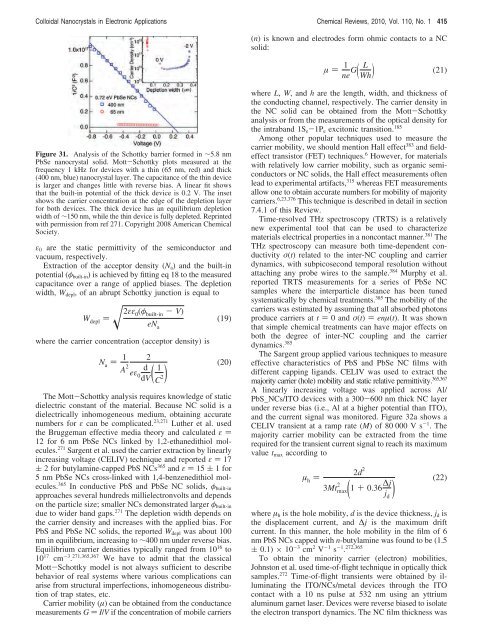
Figure 31. Analysis <strong>of</strong> the Schottky barrier <strong>for</strong>med in ∼5.8 nm<br />
PbSe nanocrystal solid. Mott-Schottky plots measured at the<br />
frequency 1 kHz <strong>for</strong> devices with a thin (65 nm, red) and thick<br />
(400 nm, blue) nanocrystal layer. The capacitance <strong>of</strong> the thin device<br />
is larger and changes little with reverse bias. A linear fit shows<br />
that the built-in potential <strong>of</strong> the thick device is 0.2 V. The inset<br />
shows the carrier concentration at the edge <strong>of</strong> the depletion layer<br />
<strong>for</strong> both devices. The thick device has an equilibrium depletion<br />
width <strong>of</strong> ∼150 nm, while the thin device is fully depleted. Reprinted<br />
with permission from ref 271. Copyright 2008 American Chemical<br />
Society.<br />
ε0 are the static permittivity <strong>of</strong> the semiconductor and<br />
vacuum, respectively.<br />
Extraction <strong>of</strong> the acceptor density (Na) and the built-in<br />
potential (φbuilt-in) is achieved by fitting eq 18 to the measured<br />
capacitance over a range <strong>of</strong> applied biases. The depletion<br />
width, Wdepl, <strong>of</strong> an abrupt Schottky junction is equal to<br />
W depl ) � 2εε 0 (φ built-in - V)<br />
eN a<br />
where the carrier concentration (acceptor density) is<br />
N a ) 1<br />
A 2<br />
eε0 2<br />
d<br />
dV( 1<br />
C 2)<br />
(19)<br />
(20)<br />
The Mott-Schottky analysis requires knowledge <strong>of</strong> static<br />
dielectric constant <strong>of</strong> the material. Because NC solid is a<br />
dielectrically inhomogeneous medium, obtaining accurate<br />
numbers <strong>for</strong> ε can be complicated. 23,271 Luther et al. used<br />
the Bruggeman effective media theory and calculated ε )<br />
12 <strong>for</strong> 6 nm PbSe NCs linked by 1,2-ethanedithiol molecules.<br />
271 Sargent et al. used the carrier extraction by linearly<br />
increasing voltage (CELIV) technique and reported ε ) 17<br />
( 2 <strong>for</strong> butylamine-capped PbS NCs 365 and ε ) 15 ( 1 <strong>for</strong><br />
5 nm PbSe NCs cross-linked with 1,4-benzenedithiol molecules.<br />
365 In conductive PbS and PbSe NC solids, φbuilt-in<br />
approaches several hundreds millielectronvolts and depends<br />
on the particle size; smaller NCs demonstrated larger φbuilt-in<br />
due to wider band gaps. 271 The depletion width depends on<br />
the carrier density and increases with the applied bias. For<br />
PbS and PbSe NC solids, the reported Wdepl was about 100<br />
nm in equilibrium, increasing to ∼400 nm under reverse bias.<br />
Equilibrium carrier densities typically ranged from 10 16 to<br />
10 17 cm -3 . 271,365,367 We have to admit that the classical<br />
Mott-Schottky model is not always sufficient to describe<br />
behavior <strong>of</strong> real systems where various complications can<br />
arise from structural imperfections, inhomogeneous distribution<br />
<strong>of</strong> trap states, etc.<br />
Carrier mobility (µ) can be obtained from the conductance<br />
measurements G ) I/V if the concentration <strong>of</strong> mobile carriers<br />
(n) is known and electrodes <strong>for</strong>m ohmic contacts to a NC<br />
solid:<br />
µ ) 1 L G( (21)<br />
ne Wh)<br />
where L, W, and h are the length, width, and thickness <strong>of</strong><br />
the conducting channel, respectively. The carrier density in<br />
the NC solid can be obtained from the Mott-Schottky<br />
analysis or from the measurements <strong>of</strong> the optical density <strong>for</strong><br />
the intraband 1Se-1Pe excitonic transition. 185<br />
Among other popular techniques used to measure the<br />
carrier mobility, we should mention Hall effect 383 and fieldeffect<br />
transistor (FET) techniques. 6 However, <strong>for</strong> materials<br />
with relatively low carrier mobility, such as organic semiconductors<br />
or NC solids, the Hall effect measurements <strong>of</strong>ten<br />
lead to experimental artifacts, 315 whereas FET measurements<br />
allow one to obtain accurate numbers <strong>for</strong> mobility <strong>of</strong> majority<br />
carriers. 6,23,376 This technique is described in detail in section<br />
7.4.1 <strong>of</strong> this Review.<br />
Time-resolved THz spectroscopy (TRTS) is a relatively<br />
new experimental tool that can be used to characterize<br />
materials electrical properties in a noncontact manner. 381 The<br />
THz spectroscopy can measure both time-dependent conductivity<br />
σ(t) related to the inter-NC coupling and carrier<br />
dynamics, with subpicosecond temporal resolution without<br />
attaching any probe wires to the sample. 384 Murphy et al.<br />
reported TRTS measurements <strong>for</strong> a series <strong>of</strong> PbSe NC<br />
samples where the interparticle distance has been tuned<br />
systematically by chemical treatments. 385 The mobility <strong>of</strong> the<br />
carriers was estimated by assuming that all absorbed photons<br />
produce carriers at t ) 0 and σ(t) ) enµ(t). It was shown<br />
that simple chemical treatments can have major effects on<br />
both the degree <strong>of</strong> inter-NC coupling and the carrier<br />
dynamics. 385<br />
The Sargent group applied various techniques to measure<br />
effective characteristics <strong>of</strong> PbS and PbSe NC films with<br />
different capping ligands. CELIV was used to extract the<br />
majority carrier (hole) mobility and static relative permittivity. 365,367<br />
A linearly increasing voltage was applied across Al/<br />
PbS_NCs/ITO devices with a 300-600 nm thick NC layer<br />
under reverse bias (i.e., Al at a higher potential than ITO),<br />
and the current signal was monitored. Figure 32a shows a<br />
CELIV transient at a ramp rate (M) <strong>of</strong>80000Vs -1 . The<br />
majority carrier mobility can be extracted from the time<br />
required <strong>for</strong> the transient current signal to reach its maximum<br />
value tmax according to<br />
µ h )<br />
2d 2<br />
2<br />
3Mtmax( 1 + 0.36∆j<br />
j ) d<br />
(22)<br />
where µh is the hole mobility, d is the device thickness, jd is<br />
the displacement current, and ∆j is the maximum drift<br />
current. In this manner, the hole mobility in the film <strong>of</strong> 6<br />
nm PbS NCs capped with n-butylamine was found to be (1.5<br />
( 0.1) × 10 -3 cm 2 V -1 s -1 . 272,365<br />
To obtain the minority carrier (electron) mobilities,<br />
Johnston et al. used time-<strong>of</strong>-flight technique in optically thick<br />
samples. 272 Time-<strong>of</strong>-flight transients were obtained by illuminating<br />
the ITO/NCs/metal devices through the ITO<br />
contact with a 10 ns pulse at 532 nm using an yttrium<br />
aluminum garnet laser. Devices were reverse biased to isolate<br />
the electron transport dynamics. The NC film thickness was


