

Prospects of Colloidal Nanocrystals for Electronic - Computer Science
Prospects of Colloidal Nanocrystals for Electronic - Computer Science
Prospects of Colloidal Nanocrystals for Electronic - Computer Science

Create successful ePaper yourself
Turn your PDF publications into a flip-book with our unique Google optimized e-Paper software.
<strong>Colloidal</strong> <strong>Nanocrystals</strong> in <strong>Electronic</strong> Applications Chemical Reviews, 2010, Vol. 110, No. 1 441<br />
conventional flash memory is extremely prone to failure <strong>of</strong><br />
insulation; one weak spot in the tunneling oxide is sufficient<br />
to create a fatal discharge path (Figure 56d). A promising<br />
way to alleviate this problem, while still preserving the<br />
fundamental operation principles <strong>of</strong> the flash memory, is to<br />
store charge not on the continuous poly silicon FG, but on<br />
a layer <strong>of</strong> discrete, mutually isolated NCs (Figure 56b). Each<br />
NC will store only few electrons; collectively, the charges<br />
stored on NCs can control the threshold voltage <strong>of</strong> the FET.<br />
The concept <strong>of</strong> distributed charge storage is more faulttolerant<br />
because minor damages in the tunnel oxide layer<br />
are not detrimental <strong>for</strong> memory operation (Figure 56e).<br />
Thinner tunneling oxide can be used to achieve lower<br />
operating voltages and/or increase the operating speed.<br />
The properties <strong>of</strong> a thin SiO2 dielectric layer can be<br />
seriously degraded under continuous memory programming<br />
(write/erase), and this severely decreases the data retention<br />
time <strong>of</strong> conventional and NC-based flash memory devices.<br />
Stability increases with increasing oxide thickness; however,<br />
thicker oxide layer reduces the tunneling current through<br />
dielectric layer, requires higher operating voltages <strong>for</strong> write/<br />
erase, and puts restrictions on down-scaling dimensions <strong>of</strong><br />
the nodes. For most flash memories, the retention time and<br />
operating speed are in inverse proportion to each other.<br />
Several approaches have been studied to achieve the fast<br />
programming speed (write/erase) and the long retention time<br />
<strong>of</strong> memory simultaneously. 583-585 Recently, researchers have<br />
focused on improving data retention time without decreasing<br />
the programing speed at low voltages. 586-588 For this purpose,<br />
it was proposed to replace the conventional SiO2 dielectric<br />
layer with a high-k gate dielectric <strong>for</strong> the control and tunnel<br />
oxide layers. High-k dielectric materials with lower conduction<br />
band <strong>of</strong>fsets with Si provide lower tunneling barriers at<br />
the dielectric channel.<br />
The idea <strong>of</strong> NC-based flash memory has been proposed<br />
in 1996 by IBM. 571,582 Since then, different metal and<br />
semiconductor NCs have been tested as FGs. 589-592 The<br />
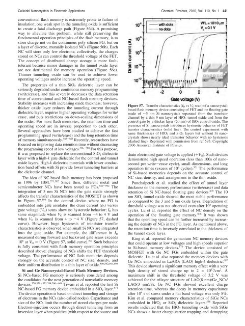
integration <strong>of</strong> 5 nm Si NCs into the gate oxide strongly<br />
affects the transfer characteristics <strong>of</strong> the MOSFET as shown<br />
in Figure 57. 593 In the control device where no FG is<br />
embedded into gate insulator, the drain current (ID) versus<br />
gate voltage (VG) scans show no hysteretic behavior; ID has<br />
same magnitude when VG is scanned from -4 to4Vand<br />
when VG is scanned from 4 to -4 V (Figure 57, dashed<br />
curve). However, huge hysteresis <strong>of</strong> transistor transfer<br />
characteristics is observed when small Si NCs are integrated<br />
into the gate oxide. For example, the difference in ID<br />
measured during <strong>for</strong>ward and backward gate scans exceeds<br />
10 6 at VG ) 0 V (Figure 57, solid curve). 593 Such behavior<br />
is fully consistent with flash memory operation principles<br />
described above; charging <strong>of</strong> NCs shifts the FET threshold<br />
voltage. The per<strong>for</strong>mance <strong>of</strong> NC flash memories depends<br />
strongly on the accurate control <strong>of</strong> NC size, density, and<br />
their uni<strong>for</strong>m distribution in a thin layer <strong>of</strong> oxide. 590,592,594,595<br />
Si and Ge Nanocrystal-Based Flash Memory Devices.<br />
Si NCs-based FG memory is seriously considered among<br />
the candidates <strong>for</strong> the next generation <strong>of</strong> nonvolatile memory<br />
devices. 370,571-573,584,596-604 Tiwari et al. reported the first Si<br />
NC-based FG memory device embedded in a SiO2 layer. 571<br />
The device operation is based on direct tunneling and storage<br />
<strong>of</strong> electrons in the NCs (also called nodes). Capacitance and<br />
size <strong>of</strong> the NCs limit the number <strong>of</strong> stored charges per node.<br />
Electron-injection occurs through direct tunneling from an<br />
inversion layer when positive (with respect to the source and<br />
Figure 57. Transfer characteristics (ID vs VG scan) <strong>of</strong> a nanocrystalbased<br />
flash memory device consisting <strong>of</strong> FET and the floating gate<br />
made <strong>of</strong> ∼5 nm Si nanocrystals separated from the transistor<br />
channel by a thin 9 nm layer <strong>of</strong> HfO2 tunnel oxide and from the<br />
control gate by a thicker layer (20 nm) <strong>of</strong> SiO2 control oxide. The<br />
presence <strong>of</strong> Si nanocrystals introduces hysteretic behavior <strong>of</strong> FET<br />
transter characteristics (solid line). The control experiment with<br />
same thicknesses <strong>of</strong> HfO2 and SiO2 layers but without Si nanocrystals<br />
shows nearly ideal transistor behavior with no hysteresis<br />
(dashed line). Reprinted with permission from ref 593. Copyright<br />
2006 American Institute <strong>of</strong> Physics.<br />
drain electrodes) gate voltage is applied (+VG). Such devices<br />
demonstrate high speed operation (less than 100s <strong>of</strong> nanosecond<br />
per write-erase cycle), small dimensions, and long<br />
operation times (excess <strong>of</strong> 10 9 cycles). 571 The per<strong>for</strong>mance<br />
<strong>of</strong> Si-based memories depends on the accurate control <strong>of</strong><br />
NC size, density, and arrangement in the thin oxide.<br />
Punchaipetch et al. studied the effect <strong>of</strong> tunnel layer<br />
thickness on the memory per<strong>for</strong>mance (write/erase) and data<br />
retention <strong>of</strong> Si NC-based floating gate devices. 605 The 10<br />
nm SiO2 tunnel oxide showed the most stable per<strong>for</strong>mance<br />
as compared to the 3 and 5 nm oxide layer. Degradation <strong>of</strong><br />
threshold voltage was not observed even after 10 8 operating<br />
cycles. Lu et al. reported the effect <strong>of</strong> NC density on the<br />
operation <strong>of</strong> the floating gate memory. 606 It was shown<br />
that the operating speed can be further increased by increasing<br />
the density <strong>of</strong> NCs in the FG layer. As mentioned above,<br />
the retention time is inversely correlated to the thickness <strong>of</strong><br />
the tunnel oxide layer.<br />
King et al. reported the gemanium NC memory devices<br />
that could operate at low voltages and high speeds superior<br />
to Si-based memory devices. 579 The device consisted <strong>of</strong><br />
MOSFET with Ge NC FGs embedded within the gate<br />
dielectric. Lu et al. also reported the memory devices with<br />
Ge NCs embedded in LaAlO3 (LAO) high-k dielectric. 607<br />
This device showed a significant memory effect with a very<br />
high density <strong>of</strong> stored charge up to 2 × 10 13 /cm 2 . A<br />
maximum shift in the threshold voltage <strong>of</strong> 3.2 V was<br />
achieved <strong>for</strong> the trilayer structure <strong>of</strong> LAO(8 nm)/Ge_NCs/<br />
LAO(3 nm)/Si. Ge NC FGs showed excellent charge<br />
retention time, whereas the decay in memory capacitance<br />
after 10 4 s <strong>of</strong> stress under a flat band voltage was only 8%.<br />
Kim et al. compared memory characteristics <strong>of</strong> SiGe NCs<br />
embedded in HfO2 or SiO2 dielectric layers. 558 Reported<br />
results indicated that the HfO2 tunneling oxide with SiGe<br />
NCs shows a faster charge carrier trapping and detrapping


