

Prospects of Colloidal Nanocrystals for Electronic - Computer Science
Prospects of Colloidal Nanocrystals for Electronic - Computer Science
Prospects of Colloidal Nanocrystals for Electronic - Computer Science

You also want an ePaper? Increase the reach of your titles
YUMPU automatically turns print PDFs into web optimized ePapers that Google loves.
<strong>Colloidal</strong> <strong>Nanocrystals</strong> in <strong>Electronic</strong> Applications Chemical Reviews, 2010, Vol. 110, No. 1 425<br />
An attenuator (a neutral density filter) is placed between the<br />
light source and chopper to study the dependence <strong>of</strong><br />
photocurrent on the intensity <strong>of</strong> incident light. Noise currents<br />
can be measured using a low-noise preamplifier and oscilloscope.<br />
Ideally, noise and leakage currents associated with<br />
the experimental setup should be eliminated wherever<br />
possible by using triaxial cables.<br />
7.2.4. Photodetectors Based on Treated Nanocrystal<br />
Solids<br />
The first detailed photoconductivity studies on TOPO-TOP<br />
capped CdSe NC solids by Leatherdale et al. 439 revealed that:<br />
(i) free carriers in CdSe NC solid originate from electron-hole<br />
pairs (excitons) photogenerated within individual NCs; (ii)<br />
charge separation was much slower as compared to the<br />
interband relaxation; and (iii) charge transport was dominated<br />
by tunneling <strong>of</strong> carriers through the interparticle medium.<br />
When studied at low temperatures, TOPO-TOP capped<br />
CdSe solids showed very low dark currents id (sub-pA range,<br />
<strong>of</strong>ten limited my measurement resolution), iph/id ≈ 10 2 , low<br />
Gi <strong>of</strong> 10 -4 , temperature-independent nonlinear I-V characteristics,<br />
and strong field-dependence <strong>of</strong> photocurrent. Large<br />
interparticle spacing, insulating nature <strong>of</strong> surface ligands, and<br />
high exciton binding energy (∼200 meV <strong>for</strong> 2 nm CdSe<br />
NCs) resulted in negligible thermally assisted separation <strong>of</strong><br />
photoexcited carriers (i.e., exciton ionization). These results<br />
were explained by the interplay <strong>of</strong> tunneling rate, charging<br />
energy, and the rates <strong>of</strong> carrier generation and recombination.<br />
To improve the interparticle charge transport, CdSe NC<br />
solids were treated with small molecular linkers: alkylamines<br />
or strong bases. 293,295 The highest photocurrents on CdSe NC<br />
solids were achieved after soaking films <strong>of</strong> TOPO-TOP<br />
capped CdSe NCs in butylamine or sodium hydroxide<br />
followed by drying at 70 °C. 293 The improvement <strong>of</strong><br />
photocurrent in this case was attributed to an increase <strong>of</strong> the<br />
exciton ionization efficiency due to an decrease in interparticle<br />
spacing and better surface passivation. With Au<br />
electrodes, Gi was limited to 1, because <strong>of</strong> the blocking nature<br />
<strong>of</strong> Au contacts to CdSe NCs (see section 6.1). Using<br />
butylamine-treated CdSe NC solids, Oertel et al. 294 fabricated<br />
photodetectors by sandwiching NC layer between ITO/<br />
PEDOT:PSS and Ag electrodes. Under illumination <strong>of</strong> 110<br />
mW/cm 2 (514 nm), devices exhibited iph/id ≈ 10 3 at zero<br />
applied bias (photovoltaic operation), and 3 dB bandwidth<br />
<strong>of</strong> 50 Hz. However, no detectivity values were reported. Gi<br />
<strong>of</strong> about 10 was achieved <strong>for</strong> CdTe NC solids prepared and<br />
treated in a similar manner. 440 In that case, high photoconductive<br />
gains were possible due to hole injection from Au<br />
contacts into CdTe NCs (injecting contacts). In CdTe NC<br />
solids, holes were found to be the majority carriers. Porter<br />
et al. fabricated primary photoconductors (i.e., no or little<br />
trap-induced photocurrents) with decreased nonradiative<br />
decay rate <strong>of</strong> the excitons using annealed and chemically<br />
treated films <strong>of</strong> core-shell CdSe/ZnS NCs. 296 They observed<br />
(i) the unity internal quantum efficiency at room temperature,<br />
(ii) the increase in the magnitude <strong>of</strong> photocurrent upon<br />
increase <strong>of</strong> temperature, and (iii) low dark currents and a 3<br />
dB bandwidth <strong>of</strong> 14 kHz.<br />
The further progress in NC-based photoconductors led to<br />
the near-IR detectors with device characteristics comparable<br />
to commercial devices. 270 In 2006, Konstantatos et al.<br />
reported simple but highly sensitive IR detectors based on<br />
PbS NCs. 265 This was also one <strong>of</strong> the first works presenting<br />
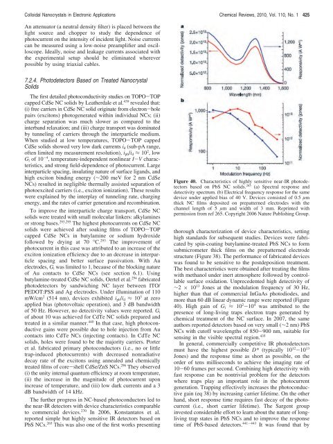
Figure 40. Characteristics <strong>of</strong> highly sensitive near-IR photodetectors<br />
based on PbS NC solids. 265 (a) Spectral response and<br />
detectivity spectrum. (b) Electrical frequency response <strong>for</strong> the same<br />
device under applied bias <strong>of</strong> 40 V. Devices consisted <strong>of</strong> 0.5 µm<br />
thick NC films deposited on prepatterned electrodes with the<br />
channel length <strong>of</strong> 5 µm and width <strong>of</strong> 3 mm. Reprinted with<br />
permission from ref 265. Copyright 2006 Nature Publishing Group.<br />
thorough characterization <strong>of</strong> device characteristics, setting<br />
high standards <strong>for</strong> subsequent studies. Devices were fabricated<br />
by spin-coating butylamine-treated PbS NCs to <strong>for</strong>m<br />
submicrometer thick films on the prepatterned electrode<br />
structure (Figure 38). The per<strong>for</strong>mance <strong>of</strong> fabricated devices<br />
was found to be sensitive to the postdeposition treatment.<br />
The best characteristics were obtained after treating the films<br />
with methanol under inert atmosphere followed by controllable<br />
surface oxidation. Unprecedented high detectivity <strong>of</strong><br />
∼2 × 10 13 Jones at the modulation frequency <strong>of</strong> 30 Hz,<br />
higher than that <strong>of</strong> commercial InGaAs photodiodes, and<br />
more than 60 dB linear dynamic range were reported (Figure<br />
40). High gain <strong>of</strong> Gi ≈ 10 2 -10 4 was attributed to the<br />
presence <strong>of</strong> long-living traps electron traps generated by<br />
chemical treatment <strong>of</strong> the NC surface. In 2007, the same<br />
authors reported detectors based on very small (∼2 nm) PbS<br />
NCs with cut<strong>of</strong>f wavelengths <strong>of</strong> 850-900 nm, suitable <strong>for</strong><br />
sensing in the visible spectral region. 435<br />
In general, commercially competitive IR photodetectors<br />
must have the highest possible D* (typically 10 12 -10 13<br />
Jones) and the response time as short as possible, on the<br />
order <strong>of</strong> tens milliseconds to achieve the imaging rate <strong>of</strong><br />
10-60 frames per second. Combining high detectivity with<br />
fast response can be nontrivial problem <strong>for</strong> the detectors<br />
where traps play an important role in the photocurrent<br />
generation. Trapping effectively increases the photoconductive<br />
gain (eq 38) by increasing carrier lifetime. On the other<br />
hand, short response time requires fast decay <strong>of</strong> the photocurrent<br />
(i.e., short carrier lifetime). The Sargent group<br />
invested considerable ef<strong>for</strong>t to learn about the nature <strong>of</strong> longliving<br />
trap states in PbS NCs and to improve the response<br />
time <strong>of</strong> PbS-based detectors. 441-443 It was found that by


