

Prospects of Colloidal Nanocrystals for Electronic - Computer Science
Prospects of Colloidal Nanocrystals for Electronic - Computer Science
Prospects of Colloidal Nanocrystals for Electronic - Computer Science

You also want an ePaper? Increase the reach of your titles
YUMPU automatically turns print PDFs into web optimized ePapers that Google loves.
<strong>Colloidal</strong> <strong>Nanocrystals</strong> in <strong>Electronic</strong> Applications Chemical Reviews, 2010, Vol. 110, No. 1 433<br />
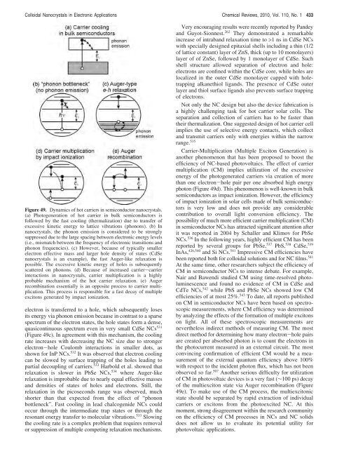
Figure 49. Dynamics <strong>of</strong> hot carriers in semiconductor nanocrystals.<br />
(a) Photogeneration <strong>of</strong> hot carrier in bulk semiconductors is<br />
followed by the fast cooling (thermalization) due to transfer <strong>of</strong><br />
excessive kinetic energy to lattice vibrations (phonons). (b) In<br />
nanocrystals, the phonon emission is considered to be strongly<br />
suppressed due to the large spacing between electronic energy levels<br />
(i.e., mismatch between the frequency <strong>of</strong> electronic transitions and<br />
phonon frequencies). (c) However, because <strong>of</strong> typically smaller<br />
electron effective mass and larger hole density <strong>of</strong> states (CdSe<br />
nanocrystals is an example), the fast Auger-like relaxation is<br />
possible. The excessive kinetic energy <strong>of</strong> holes is subsequently<br />
scattered on phonons. (d) Because <strong>of</strong> increased carrier-carrier<br />
interactions in nanocrystals, carrier multiplication is a highly<br />
probable mechanism <strong>of</strong> the hot carrier relaxation. (e) Auger<br />
recombination essentially is an opposite process to carrier multiplication.<br />
This process is responsible <strong>for</strong> a fast decay <strong>of</strong> multiple<br />
excitons generated by impact ionization.<br />
electron is transferred to a hole, which subsequently loses<br />
its energy via phonon emission because in contrast to a sparse<br />
spectrum <strong>of</strong> the electron states, the hole states <strong>for</strong>m a dense,<br />
quasicontinuous spectrum even in very small CdSe NCs 531<br />
(Figure 49c). In agreement with this mechanism, the cooling<br />
rate increases with decreasing the NC size due to stronger<br />
electron-hole Coulomb interactions in smaller dots, as<br />
shown <strong>for</strong> InP NCs. 532 It was observed that electron cooling<br />
can be slowed by surface trapping <strong>of</strong> the holes leading to<br />
partial decoupling <strong>of</strong> carriers. 533 Harbold et al. showed that<br />
relaxation is slower in PbSe NCs, 534 where Auger-like<br />
relaxation is improbable due to nearly equal effective masses<br />
and densities <strong>of</strong> states <strong>of</strong> holes and electrons. Still, the<br />
relaxation in the picoseconds range was observed, much<br />
shorter than that expected from the effect <strong>of</strong> “phonon<br />
bottleneck”. Fast cooling in lead chalcogenide NCs could<br />
occur through the intermediate trap states or through the<br />
resonant energy transfer to molecular vibrations. 533 Slowing<br />
the cooling rate is a complex problem that requires removal<br />
or suppression <strong>of</strong> multiple competing relaxation mechanisms.<br />
Very encouraging results were recently reported by Pandey<br />
and Guyot-Sionnest. 262 They demonstrated a remarkable<br />
increase <strong>of</strong> intraband relaxation time to >1 ns in CdSe NCs<br />
with specially designed epitaxial shells including a thin (1/2<br />
<strong>of</strong> lattice constant) layer <strong>of</strong> ZnS, thick (up to 10 monolayers)<br />
layer <strong>of</strong> <strong>of</strong> ZnSe, followed by 1 monolayer <strong>of</strong> CdSe. Such<br />
shell structure allowed separation <strong>of</strong> electron and hole:<br />
electrons are confined within the CdSe core, while holes are<br />
localized in the outer CdSe monolayer capped with holetrapping<br />
alkanethiol ligands. The presence <strong>of</strong> CdSe outer<br />
layer and thiol surface ligands also prevents surface trapping<br />
<strong>of</strong> electrons.<br />
Not only the NC design but also the device fabrication is<br />
a highly challenging task <strong>for</strong> hot carrier solar cells. The<br />
separation and collection <strong>of</strong> carriers has to be faster than<br />
their thermalization. One suggested design <strong>of</strong> hot carrier cell<br />
implies the use <strong>of</strong> selective energy contacts, which collect<br />
and transmit carriers only with energies within the narrow<br />
range. 535<br />
Carrier-Multiplication (Multiple Exciton Generation) is<br />
another phenomenon that has been proposed to boost the<br />
efficiency <strong>of</strong> NC-based photovoltaics. The effect <strong>of</strong> carrier<br />
multiplication (CM) implies utilization <strong>of</strong> the excessive<br />
energy <strong>of</strong> the photogenerated carriers via creation <strong>of</strong> more<br />
than one electron-hole pair per one absorbed high energy<br />
photon (Figure 49d). This phenomenon is well-known in bulk<br />
semiconductors as impact ionization. However, the efficiency<br />
<strong>of</strong> impact ionization in solar cells made <strong>of</strong> bulk semiconductors<br />
is very low and does not provide any considerable<br />
contribution to overall light conversion efficiency. The<br />
possibility <strong>of</strong> much more efficient carrier multiplication (CM)<br />
in semiconductor NCs has attracted significant attention after<br />
it was reported in 2004 by Schaller and Klimov <strong>for</strong> PbSe<br />
NCs. 536 In the following years, highly efficient CM has been<br />
reported by several groups <strong>for</strong> PbSe, 537 PbS, 538 CdSe, 539<br />
InAs, 426,540 and Si NCs. 541 Impressive CM efficiencies have<br />
been reported both <strong>for</strong> colloidal solutions and <strong>for</strong> NC films. 541<br />
At the same time, other researchers subject the efficiency <strong>of</strong><br />
CM in semiconductor NCs to intense debate. For example,<br />
Nair and Bawendi studied CM using time-resolved photoluminescence<br />
and found no evidence <strong>of</strong> CM in CdSe and<br />
CdTe NCs, 542 while PbS and PbSe NCs showed low CM<br />
efficiencies <strong>of</strong> at most 25%. 543 To date, all reports published<br />
on CM in semiconductor NCs have been based on spectroscopic<br />
measurements, where CM efficiency was determined<br />
by analyzing the effects <strong>of</strong> the <strong>for</strong>mation <strong>of</strong> multiple excitons<br />
on light. All <strong>of</strong> these spectroscopic measurements are<br />
nevertheless indirect methods <strong>of</strong> measuring CM. The most<br />
direct method <strong>for</strong> determining how many electron-hole pairs<br />
are created per absorbed photon is to count the electrons in<br />
the photocurrent measured in an external circuit. The most<br />
convincing confirmation <strong>of</strong> efficient CM would be a measurement<br />
<strong>of</strong> the external quantum efficiency above 100%<br />
with respect to the incident photon flux, which has not been<br />
observed so far. 507 Another serious difficulty <strong>for</strong> utilization<br />
<strong>of</strong> CM in photovoltaic devices is a very fast (∼100 ps) decay<br />
<strong>of</strong> the multiexciton state via Auger recombination (Figure<br />
49e). To make use <strong>of</strong> the CM process, the multiexcitonic<br />
state should be separated by rapid extraction <strong>of</strong> individual<br />
carriers or excitons from the photoexcited NC. At this<br />
moment, strong disagreement within the research community<br />
on the efficiency <strong>of</strong> CM processes in NCs and NC solids<br />
does not allow us to evaluate its potential utility <strong>for</strong><br />
photovoltaic applications.


