

Prospects of Colloidal Nanocrystals for Electronic - Computer Science
Prospects of Colloidal Nanocrystals for Electronic - Computer Science
Prospects of Colloidal Nanocrystals for Electronic - Computer Science

You also want an ePaper? Increase the reach of your titles
YUMPU automatically turns print PDFs into web optimized ePapers that Google loves.
<strong>Colloidal</strong> <strong>Nanocrystals</strong> in <strong>Electronic</strong> Applications Chemical Reviews, 2010, Vol. 110, No. 1 405<br />
As a result, a high-mobility SnS2 compound is <strong>for</strong>med<br />
around the NCs. In this case, the surface ligands act not only<br />
as a tunable spacer and potential barrier between NC, but<br />
participate in the charge transport. For example, field-effect<br />
transistors have been assembled from 5 nm CdSe NCs<br />
stabilized with 5 wt % <strong>of</strong> (N2H5)4Sn2S6, annealed at 200<br />
°C. 273 A similar approach based on MCC ligands can be used<br />
to integrate colloidal NCs into different metal chalcogenide<br />
matrices such as In2Se3,In2Te3,Ga2Se3, HgSe, ZnTe, Bi2Te3,<br />
and CuInxGa1-xSe2. Combined with the diversity <strong>of</strong> properly<br />
engineered colloidal NCs, we expect a rapid development<br />
<strong>of</strong> many novel all-inorganic nanocomposites <strong>for</strong> electronic,<br />
photovoltaic, and thermoelectric applications.<br />
5. Transport in Nanocrystal Solids<br />
Generally speaking, the NC solids represent a class <strong>of</strong><br />
artificial materials composed <strong>of</strong> close-packed metal or<br />
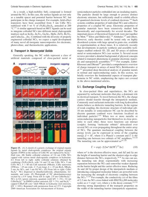
Figure 15. (A) A sketch <strong>of</strong> a generic exchange <strong>of</strong> original organic<br />
ligands by metal chalcogenide complexes: the original organic<br />
ligands (TOPO) at the surface <strong>of</strong> CdSe NC are replaced by Sn2S6 4-<br />
Zintl ions. (B) Stable colloidal solutions <strong>of</strong> 3.6 nm CdSe NCs<br />
capped with various metal chalcogenide complexes in hydrazine.<br />
(C) From left to right: stable colloidal solutions obtained by<br />
combining (N2H5)4Sn2S6 with 3.6 and 5.8 nm CdSe NCs, 9 nm<br />
CdTe NCs, 5 × 60 nm CdS nanorods (NRods), CdSe nanowires<br />
(NWires, ∼25 nm wide, 2-5 µm long), 6 × 25 nm Bi2S3 NRods,<br />
5 nm Au NCs, and 3 nm Pd NCs. (D) From left to right: CdSe/<br />
Sn2S6 4- NCs dispersed in dimethylsulfoxide, ethanolamine, <strong>for</strong>mamide,<br />
and water. (E) Photograph <strong>of</strong> NC photoluminescence<br />
excited by a UV lamp. From left to right: 2.9 nm CdSe/Sn2S6 4-<br />
NCs in EA (green emission, quantum yield QY ≈ 2%), 3.6 nm<br />
CdSe/Sn2S6 4- in DMSO (yellow emission, QY ≈ 3%), and Sn2S6 4- -<br />
capped CdSe/CdS core-shell NRods in hydrazine (red emission,<br />
QY ) 10%). Reprinted with permission from ref 273. Copyright<br />
2009 American Association <strong>for</strong> Advancement <strong>of</strong> <strong>Science</strong>.<br />
semiconductor particles embedded into an insulating matrix.<br />
The particles should be large enough to possess distinct<br />
electronic structure, but sufficiently small to exhibit effects<br />
<strong>of</strong> quantized electronic levels <strong>of</strong> confined electrons. 314 Such<br />
systems combine properties <strong>of</strong> individual NCs and collective<br />
properties <strong>of</strong> a coupled NC array. <strong>Electronic</strong> properties <strong>of</strong><br />
granular materials have been extensively studied both<br />
theoretically and experimentally <strong>for</strong> several decades. The<br />
important pieces <strong>of</strong> theoretical framework were put together<br />
by Mott, 315 Efros and Shklovskii, 316 Altshuler, 317 and others.<br />
However, early theories could be tested only on highly<br />
disordered systems with large spread in grain size, available<br />
to experimentalists at those times. It is relatively recently<br />
that developments in particle synthesis and assembly techniques<br />
enabled ordered 1D, 2D, and 3D arrays <strong>of</strong> uni<strong>for</strong>m<br />
metal or semiconductor NCs (see section 3). Several recent<br />
reviews provided a detailed background <strong>of</strong> physical concepts<br />
related to transport phenomena in granular electronic materials<br />
and nanoparticle assemblies. 267,318 For example, Zabet-<br />
Khosousi and Dhirani 267 provided a comprehensive overview<br />
<strong>of</strong> charge transport in arrays <strong>of</strong> metal NCs; Beloborodov et<br />
al. 314 presented deep theoretical analysis <strong>of</strong> granular metals<br />
in normal and superconducting states. In this section, we<br />
briefly overview the fundamental aspects <strong>of</strong> transport phenomena<br />
in NC solids, emphasizing the topics not covered<br />
in the above-mentioned articles.<br />
5.1. Exchange Coupling Energy<br />
In close-packed films and superlattices, the NCs are<br />
separated by surfactant molecules that play a dominant role<br />
in electrical transport. To travel between the NCs, the charge<br />
carriers should transfer through the interparticle medium.<br />
Commonly used surfactant molecules with long hydrocarbon<br />
chains behave as dielectric tunneling barriers. In the regime<br />
<strong>of</strong> weak coupling, the electronic structure <strong>of</strong> individual sub-<br />
10 nm metallic or semiconductor NC can be described by<br />
discrete quantum confined wave functions localized on<br />
individual particles3,318 When two or more metallic or<br />
semiconducting nanoparticles find themselves in close proximity<br />
to each other, these wave functions can interact<br />
(couple), <strong>for</strong>ming “molecular orbitals” delocalized over<br />
several NCs or even propagating throughout the entire array<br />
<strong>of</strong> NCs. The quantum mechanical coupling between the<br />
energy levels can be expressed in terms <strong>of</strong> the coupling<br />
energy � ≈ hΓ, where h is Planck’s constant and Γ is the<br />
tunneling rate between two orbitals <strong>of</strong> NC neighbors. 319,320<br />
The tunneling rate can be approximated as267,320 Γ ≈ exp{–2(2m*∆E/p 2 ) 1/2 ∆x} (10)<br />
where m* is the electron effective mass, and ∆E and ∆x are<br />
the height <strong>of</strong> tunneling barrier and the shortest edge-to-edge<br />
distance between the NCs, respectively. 38,39 As one can see,<br />
the tunneling rate drops exponentially with increasing<br />
separation between the NCs and somewhat weaker depends<br />
on the barrier height and the carrier effective mass. Reducing<br />
∆x and ∆E by proper design <strong>of</strong> the interparticle medium or<br />
introducing conjugated molecular linkers are powerful tools<br />
<strong>for</strong> increasing the strength <strong>of</strong> electronic coupling between<br />
the NCs. 23,185 For example, the conductivity (σ) <strong>of</strong> the films<br />
<strong>of</strong> 2.2 nm Au NCs cross-linked with HS(CH2)nSH molecules<br />
scales as σ ≈ exp(-κn), where κ is the decay constant, 321,322<br />
showing strong dependence <strong>of</strong> the transport properties on<br />
the width <strong>of</strong> the tunneling barrier (interparticle separation).


