

Prospects of Colloidal Nanocrystals for Electronic - Computer Science
Prospects of Colloidal Nanocrystals for Electronic - Computer Science
Prospects of Colloidal Nanocrystals for Electronic - Computer Science

You also want an ePaper? Increase the reach of your titles
YUMPU automatically turns print PDFs into web optimized ePapers that Google loves.
410 Chemical Reviews, 2010, Vol. 110, No. 1 Talapin et al.<br />
are maximally disordered. For fields beyond Hc, the resistance<br />
again decreases to the initial value 335 (Figure 25b). With<br />
increasing temperature above 2 K, MR decreases rapidly due<br />
to spin-flip scattering, down to ∼10% <strong>of</strong> its maximum value<br />
at 20 K. At very low temperatures, the cotunneling processes<br />
can result in significant enhancement <strong>of</strong> MR. 339<br />
Larger values <strong>of</strong> MR can be achieved with the class <strong>of</strong><br />
materials called half-metals. A half-metal is characterized<br />
by the presence <strong>of</strong> an energy gap at the Fermi level <strong>for</strong> only<br />
one electron spin direction, while the energy band <strong>for</strong> the<br />
opposite spin direction is continuous. 340 Such band structure<br />
leads to P ) 1 and theoretical ∆R/Rmax values <strong>of</strong> 100% and<br />
50% <strong>for</strong> antiparallel and random spin orientations at H ) 0,<br />
correspondingly. Magnetite Fe3O4 is the example <strong>of</strong> a halfmetal.<br />
Recently, Zeng et al. reported appreciable 20-35%<br />
MR values at T ) 60 K <strong>for</strong> a superlattice <strong>of</strong> 6 nm diameter<br />
Fe3O4 NCs. 341 (Figure 25c). At room temperature, MR <strong>of</strong><br />
Fe3O4 NC solids remained as large as 12%. For comparison,<br />
room temperature MR <strong>of</strong> magnetite thin films does not<br />
exceed a few percent. 341<br />
The presence <strong>of</strong> a very large number <strong>of</strong> tunneling junctions<br />
in a weakly coupled NC solid has several advantageous<br />
effects on spin-dependent electronic transport. Because<br />
current through the NC array is carried by multiple parallel<br />
conduction paths containing different numbers <strong>of</strong> NCs, the<br />
device MR should be less sensitive to applied bias voltage. 342<br />
Indeed, both Co and Fe3O4 NC solids demonstrated weak<br />
dependence <strong>of</strong> magnetoresistance on the applied voltage, in<br />
contrast to thin film devices that <strong>of</strong>ten show steep reduction<br />
in MR with increasing bias. 334,341 This advantage may help<br />
NC arrays to find use in magnetic recording heads and<br />
nonvolatile magnetoresistive random access memory (MRAM)<br />
applications. 343 However, further developments in understanding<br />
and improving spin-dependent electronic properties<br />
are necessary to successfully compete with more mature<br />
technologies based on vacuum-deposited thin films and<br />
heterostructures. The possibility <strong>of</strong> combining magnetic NCs<br />
with other materials, <strong>for</strong> example, semiconductor quantum<br />
dots in <strong>for</strong>m <strong>of</strong> multicomponent nanostructures (Figure 6)<br />
or binary superlattices (Figure 11), may lead to interesting<br />
multifunctional electronic materials.<br />
5.6. Semiconductor <strong>Nanocrystals</strong>: <strong>Electronic</strong><br />
Structure and Shell Filling<br />
Semiconductor NCs represent probably the most interesting<br />
and important class <strong>of</strong> inorganic solution processed<br />
electronic materials. They have a real chance to find use<br />
in the next generations <strong>of</strong> large area solar cells and lightemitting<br />
devices. Fundamental understanding <strong>of</strong> charge<br />
transport is also crucial <strong>for</strong> developments <strong>of</strong> NC-based<br />
electrically pumped lasers, low-dimensional thermoelectric<br />
materials, 254 photodetectors, 265,294 and many other technologies.<br />
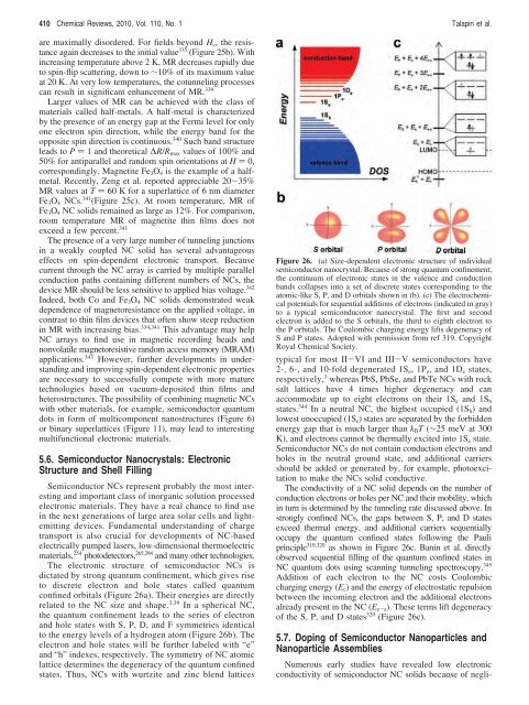
The electronic structure <strong>of</strong> semiconductor NCs is<br />
dictated by strong quantum confinement, which gives rise<br />
to discrete electron and hole states called quantum<br />
confined orbitals (Figure 26a). Their energies are directly<br />
related to the NC size and shape. 3,39 In a spherical NC,<br />
the quantum confinement leads to the series <strong>of</strong> electron<br />
and hole states with S, P, D, and F symmetries identical<br />
to the energy levels <strong>of</strong> a hydrogen atom (Figure 26b). The<br />
electron and hole states will be further labeled with “e”<br />
and “h” indexes, respectively. The symmetry <strong>of</strong> NC atomic<br />
lattice determines the degeneracy <strong>of</strong> the quantum confined<br />
states. Thus, NCs with wurtzite and zinc blend lattices<br />
typical <strong>for</strong> most II-VI and III-V semiconductors have<br />
2-, 6-, and 10-fold degenerated 1Se, 1Pe, and 1De states,<br />
respectively, 3 whereas PbS, PbSe, and PbTe NCs with rock<br />
salt lattices have 4 times higher degeneracy and can<br />
accommodate up to eight electrons on their 1Se and 1Sh<br />
states. 344 In a neutral NC, the highest occupied (1Sh) and<br />
lowest unoccupied (1Se) states are separated by the <strong>for</strong>bidden<br />
energy gap that is much larger than kBT (∼25 meV at 300<br />
K), and electrons cannot be thermally excited into 1Se state.<br />
Semiconductor NCs do not contain conduction electrons and<br />
holes in the neutral ground state, and additional carriers<br />
should be added or generated by, <strong>for</strong> example, photoexcitation<br />
to make the NCs solid conductive.<br />
The conductivity <strong>of</strong> a NC solid depends on the number <strong>of</strong><br />
conduction electrons or holes per NC and their mobility, which<br />
in turn is determined by the tunneling rate discussed above. In<br />
strongly confined NCs, the gaps between S, P, and D states<br />
exceed thermal energy, and additional carriers sequentially<br />
occupy the quantum confined states following the Pauli<br />
principle319,320 as shown in Figure 26c. Banin et al. directly<br />
observed sequential filling <strong>of</strong> the quantum confined states in<br />
NC quantum dots using scanning tunneling spectroscopy. 345<br />
Addition <strong>of</strong> each electron to the NC costs Coulombic<br />
charging energy (Ec) and the energy <strong>of</strong> electrostatic repulsion<br />
between the incoming electron and the additional electrons<br />
already present in the NC (Ee-e). These terms lift degeneracy<br />
<strong>of</strong> the S, P, and D states320 Figure 26. (a) Size-dependent electronic structure <strong>of</strong> individual<br />
semiconductor nanocrystal. Because <strong>of</strong> strong quantum confinement,<br />
the continuum <strong>of</strong> electronic states in the valence and conduction<br />
bands collapses into a set <strong>of</strong> discrete states corresponding to the<br />
atomic-like S, P, and D orbitals shown in (b). (c) The electrochemical<br />
potentials <strong>for</strong> sequential additions <strong>of</strong> electrons (indicated in gray)<br />
to a typical semiconducotor nanocrystal. The first and second<br />
electron is added to the S orbitals, the third to eighth electron to<br />
the P orbitals. The Coulombic charging energy lifts degeneracy <strong>of</strong><br />
S and P states. Adopted with permission from ref 319. Copyright<br />
Royal Chemical Society.<br />
(Figure 26c).<br />
5.7. Doping <strong>of</strong> Semiconductor Nanoparticles and<br />
Nanoparticle Assemblies<br />
Numerous early studies have revealed low electronic<br />
conductivity <strong>of</strong> semiconductor NC solids because <strong>of</strong> negli-


