

Prospects of Colloidal Nanocrystals for Electronic - Computer Science
Prospects of Colloidal Nanocrystals for Electronic - Computer Science
Prospects of Colloidal Nanocrystals for Electronic - Computer Science

You also want an ePaper? Increase the reach of your titles
YUMPU automatically turns print PDFs into web optimized ePapers that Google loves.
<strong>Colloidal</strong> <strong>Nanocrystals</strong> in <strong>Electronic</strong> Applications Chemical Reviews, 2010, Vol. 110, No. 1 439<br />
The per<strong>for</strong>mance <strong>of</strong> FET devices assembled <strong>of</strong> ZnO<br />
nanorods was further enhanced by the postdeposition hydrothermal<br />
growth step when a thin layer <strong>of</strong> ZnO was<br />
chemically deposited into the voids between ZnO nanorods.<br />
563 After such treatment was followed by the annealing<br />
step in hydrogen atmosphere, the devices achieved mobility<br />
values <strong>of</strong> 1.2-1.4 cm 2 V -1 s -1 and an Ion/I<strong>of</strong>f ratio <strong>of</strong> 10 6 -10 7 .<br />
These mobility values, combined with optical transparency<br />
and solution-based fabrication, have a good chance to pave<br />
the way <strong>for</strong> ZnO NC FETs into commercial applications.<br />
The next interesting step in development <strong>of</strong> NC-based<br />
FETs was to combine multiple functionalities using engineered<br />
multicomponent NCs as the building blocks <strong>for</strong><br />
transistor channel. Recent developments in the colloidal<br />
synthesis <strong>of</strong> inorganic nanostructures allowed exciting opportunities<br />
<strong>for</strong> cointegration <strong>of</strong> materials with different<br />
functionalities in <strong>for</strong>m <strong>of</strong> core-shell, dumbbell, and other<br />
nanostructures (see section 2). In 2008, Lee et al. demonstrated<br />
FETs employing multifunctional NCs, core-shell<br />
particles with plasmonic Au core and semiconducting PbS<br />
shell (Figure 28c,d). 24 The intraparticle charge transfer<br />
between Au core and PbS shell <strong>for</strong>med the charge-transfer<br />
complex resulting in p-type doping <strong>of</strong> the FET channel. Later,<br />
Lee et al. demonstrated FETs combining semiconductor and<br />
magnetic functionalities. Specifically, they used core-shell<br />
and dumbbell nanostructures combining FePt and PbS or<br />
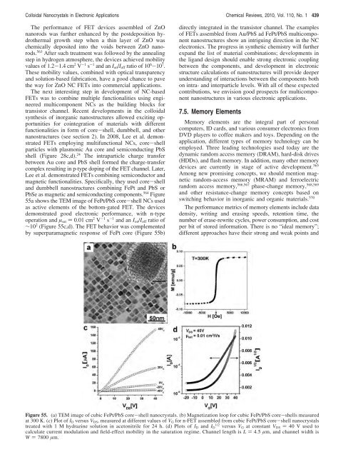
PbSe as magnetic and semiconducting components. 564 Figure<br />
55a shows the TEM image <strong>of</strong> FePt/PbS core-shell NCs used<br />
as active elements <strong>of</strong> the bottom-gated FET. The devices<br />
demonstrated good electronic per<strong>for</strong>mance, with n-type<br />
operation and µsat ) 0.01 cm 2 V -1 s -1 and an Ion/I<strong>of</strong>f ratio <strong>of</strong><br />
∼10 2 (Figure 55c,d). The FET behavior was complemented<br />
by superparamagnetic response <strong>of</strong> FePt core (Figure 55b)<br />
directly integrated in the transistor channel. The examples<br />
<strong>of</strong> FETs assembled from Au/PbS ad FePt/PbS multicomponent<br />
nanostructures show an intriguing direction in the NC<br />
electronics. The progress in synthetic chemistry will further<br />
expand the list <strong>of</strong> material combinations; developments in<br />
the ligand design should enable strong electronic coupling<br />
between the components, and development in electronic<br />
structure calculations <strong>of</strong> nanostructures will provide deeper<br />
understanding <strong>of</strong> interactions between the components both<br />
on intra- and interparticle levels. With all <strong>of</strong> these expected<br />
contributions, we envision good prospects <strong>for</strong> multicomponent<br />
nanostructures in various electronic applications.<br />
7.5. Memory Elements<br />
Memory elements are the integral part <strong>of</strong> personal<br />
computers, ID cards, and various consumer electronics from<br />
DVD players to c<strong>of</strong>fee makers and toys. Depending on the<br />
application, different types <strong>of</strong> memory technology can be<br />
employed. Three leading technologies used today are the<br />
dynamic random access memory (DRAM), hard-disk drives<br />
(HDDs), and flash memory. In addition, many other memory<br />
devices are currently in stage <strong>of</strong> active development. 565<br />
Among new promising concepts, we should mention magnetic<br />
random-access memory (MRAM) and ferroelectric<br />
random access memory, 566,567 phase-change memory, 568,569<br />
and other resistance-change memory concepts based on<br />
switching behavior in inorganic and organic materials. 570<br />
The per<strong>for</strong>mance metrics <strong>of</strong> memory elements include data<br />
density, writing and erasing speeds, retention time, the<br />
number <strong>of</strong> erase-rewrite cycles, power consumption, and cost<br />
per bit <strong>of</strong> stored in<strong>for</strong>mation. There is no “ideal memory”;<br />
different approaches have their strong and weak points and<br />
Figure 55. (a) TEM image <strong>of</strong> cubic FePt/PbS core-shell nanocrystals. (b) Magnetization loop <strong>for</strong> cubic FePt/PbS core-shells measured<br />
at 300 K. (c) Plot <strong>of</strong> ID versus VDS, measured at different values <strong>of</strong> VG <strong>for</strong> n-FET assembled from cubic FePt/PbS core-shell nanocrystals<br />
treated with 1 M hydrazine solution in acetonitrile <strong>for</strong> 24 h. (d) Plots <strong>of</strong> ID and ID 1/2 versus VG at constant VDS ) 40 V used to<br />
calculate current modulation and field-effect mobility in the saturation regime. Channel length is L ) 4.5 µm, and channel width is<br />
W ) 7800 µm.


