

Prospects of Colloidal Nanocrystals for Electronic - Computer Science
Prospects of Colloidal Nanocrystals for Electronic - Computer Science
Prospects of Colloidal Nanocrystals for Electronic - Computer Science

Create successful ePaper yourself
Turn your PDF publications into a flip-book with our unique Google optimized e-Paper software.
<strong>Colloidal</strong> <strong>Nanocrystals</strong> in <strong>Electronic</strong> Applications Chemical Reviews, 2010, Vol. 110, No. 1 427<br />
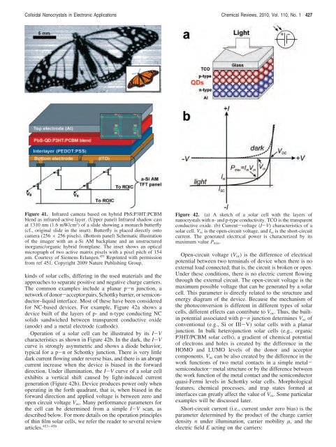
Figure 41. Infrared camera based on hybrid PbS:P3HT:PCBM<br />
blend as infrared-active layer. (Upper panel) Infrared shadow cast<br />
at 1310 nm (1.6 mW/cm 2 ) <strong>of</strong> a slide showing a monarch butterfly<br />
(cf., original slide in the inset). Butterfly is placed directly onto<br />
camera (256 × 256 pixels). (Bottom panel) Schematic illustration<br />
<strong>of</strong> the imager with an a-Si AM backplane and an unstructured<br />
inorganic/organic hybrid frontplane. The inset shows an optical<br />
micrograph <strong>of</strong> two active matrix pixels with a pixel pitch <strong>of</strong> 154<br />
µm. Courtesy <strong>of</strong> Siemens Erlangen. 451 Reprinted with permission<br />
from ref 451. Copyright 2009 Nature Publishing Group.<br />
kinds <strong>of</strong> solar cells, differing in the used materials and the<br />
approaches to separate positive and negative charge carriers.<br />
The common examples include a planar p-n junction, a<br />
network <strong>of</strong> donor-acceptor pairs, Schottky barrier, or semiconductor–liquid<br />
interface. Most <strong>of</strong> these have been considered<br />
<strong>for</strong> NC-based devices. For example, Figure 42a shows a<br />
device built <strong>of</strong> the layers <strong>of</strong> p- and n-type conducting NC<br />
solids sandwiched between transparent conductive oxide<br />
(anode) and a metal electrode (cathode).<br />
Operation <strong>of</strong> a solar cell can be illustrated by its I-V<br />
characteristics as shown in Figure 42b. In the dark, the I-V<br />
curve is strongly asymmetric and shows a diode behavior,<br />
typical <strong>for</strong> a p-n or Schottky junction. There is very little<br />
dark current flowing under reverse bias, and there is an abrupt<br />
current increase when the device is biased in the <strong>for</strong>ward<br />
direction. Under illumination, the I-V curve <strong>of</strong> a solar cell<br />
exhibits a vertical shift caused by light-induced current<br />
generation (Figure 42b). Device produces power only when<br />
operating in the <strong>for</strong>th quadrant, that is, when biased in the<br />
<strong>for</strong>ward direction and applied voltage is between zero and<br />
open circuit voltage Voc. Many per<strong>for</strong>mance parameters <strong>for</strong><br />
the cell can be determined from a simple I-V scan, as<br />
described below. For more details on the operation principles<br />
<strong>of</strong> thin film solar cells, we refer the reader to several review<br />
articles. 453-456<br />
Figure 42. (a) A sketch <strong>of</strong> a solar cell with the layers <strong>of</strong><br />
nanocrystals with n- and p-type conductivity. TCO is the transparent<br />
conductive oxide. (b) Current-voltage (I-V) characteristics <strong>of</strong> a<br />
solar cell. Voc is the open-circuit voltage, and Isc is the short-circuit<br />
current. The generated electrical power is characterized by its<br />
maximum value Pmax.<br />
Open-circuit voltage (Voc) is the difference <strong>of</strong> electrical<br />
potential between two terminals <strong>of</strong> device when there is no<br />
external load connected; that is, the circuit is broken or open.<br />
Under these conditions, there is no electric current flowing<br />
through the external circuit. The open-circuit voltage is the<br />
maximum possible voltage that can be generated by a solar<br />
cell. This parameter is directly related to the structure and<br />
energy diagram <strong>of</strong> the device. Because the mechanism <strong>of</strong><br />
the photoconversion is different in different types <strong>of</strong> solar<br />
cells, different effects can contribute to Voc. Thus, the builtin<br />
potential associated with p-n junction determines Voc <strong>of</strong><br />
conventional (e.g., Si or III-V) solar cells with a planar<br />
junction. In bulk heterojunction solar cells (e.g., organic<br />
P3HT/PCBM solar cells), a gradient <strong>of</strong> chemical potential<br />
<strong>of</strong> electrons and holes is created by the difference in the<br />
HOMO and LUMO levels <strong>of</strong> the donor and acceptor<br />
components. Voc can be also created by the difference in the<br />
work functions <strong>of</strong> two metal contacts in a simple metalsemiconductor-metal<br />
structure or by the difference between<br />
the work function <strong>of</strong> the metal contact and the semiconductor<br />
quasi-Fermi levels in Schottky solar cells. Morphological<br />
features, chemical processes, and trap states <strong>for</strong>med at<br />
interfaces can greatly affect the value <strong>of</strong> Voc. Some particular<br />
examples will be discussed later.<br />
Short-circuit current (i.e., current under zero bias) is the<br />
parameter determined by the product <strong>of</strong> the charge carrier<br />
density n under illumination, carrier mobility µ, and the<br />
electric field E acting on the carriers:


