

Prospects of Colloidal Nanocrystals for Electronic - Computer Science
Prospects of Colloidal Nanocrystals for Electronic - Computer Science
Prospects of Colloidal Nanocrystals for Electronic - Computer Science

You also want an ePaper? Increase the reach of your titles
YUMPU automatically turns print PDFs into web optimized ePapers that Google loves.
442 Chemical Reviews, 2010, Vol. 110, No. 1 Talapin et al.<br />
at low voltages even when the oxide thickness was slightly<br />
thicker than that <strong>for</strong> SiO2 tunneling oxide memory.<br />
Metal Nanocrystal-Based Flash Memory Devices. Recently,<br />
it was realized that flash memory devices using metal<br />
NCs as floating gates can be superior to the devices utilizing<br />
semiconductor NCs. 576-578,586-589,591,608-611 The advantages <strong>of</strong><br />
metal NCs <strong>for</strong> memory applications are higher density <strong>of</strong><br />
states near the Fermi level, stronger electrostatic coupling<br />
to the conducting channel, tunable work function, and small<br />
energy perturbations due to carrier confinement. The work<br />
function can be tuned by using different metals and metal<br />
alloys <strong>of</strong>fering an opportunity to optimize the trade-<strong>of</strong>f<br />
between write/erase speed and charge retention because the<br />
work function <strong>of</strong> NC FGs controls not only the depth <strong>of</strong> the<br />
potential well at the storage node but also the density <strong>of</strong> states<br />
available <strong>for</strong> carrier tunneling. Numerous attempts have been<br />
made to develop nonvolatile memory devices using <strong>for</strong> FG<br />
metal NCs such as Au, Pt, Ni, Co, Ag, etc. 589,591,592 So far,<br />
Au is one <strong>of</strong> the most promising materials because it is<br />
chemically stable and has a large work function. Isolated<br />
Au NCs <strong>for</strong>m a deep quantum well between the control oxide<br />
and tunnel oxide, desirable <strong>for</strong> the FG application.<br />
For example, Chan et al. reported the memory characteristics<br />
<strong>of</strong> Au NCs embedded in the amorphous HfAlO tunnel<br />
layer. 587 A significant threshold voltage shift was obtained<br />
due to charge trapping on Au NCs. The memory window<br />
and stored charge density were ∼10 V and ∼1 × 10 14 /cm 2 ,<br />
respectively. A smaller size <strong>of</strong> Au NCs showed a higher<br />
tunneling coefficient and a larger memory window. Lo et<br />
al. reported charge storage characteristics <strong>of</strong> Au NCs on the<br />
multistacked layer <strong>of</strong> Al2O3/HfO2/SiO2. 588 The device showed<br />
high efficiencies <strong>of</strong> charge injection and detrapping with long<br />
retention times. There are several good review articles on<br />
metal NCs-based memory devices. 589,591,592,612,613<br />
All above-described devices employed metal and semiconductor<br />
NCs deposited from the gas phase using CVD or<br />
high-vacuum deposition techniques. Such processes typically<br />
have difficulties with controlling NC size and packing<br />
density. In addition, high temperature processes <strong>for</strong> making<br />
NCs can provide a source <strong>of</strong> metallic contamination due to<br />
diffusion <strong>of</strong> metal atoms into FET channel. <strong>Colloidal</strong><br />
synthesis <strong>of</strong> NCs provides a convenient opportunity to<br />
overcome many problems <strong>of</strong> gas-phase NC growth. It can<br />
easily provide monodisperse NCs <strong>of</strong> different materials with<br />
precisely tunable size. The NCs can be integrated into the<br />
memory device using low temperature solution processing.<br />
Recently, memory devices using colloidal NCs as chargetrapping<br />
elements have been reported. 614-622 Park et al.<br />
reported the memory effects <strong>for</strong> colloidal gold NCs embedded<br />
between thermally grown SiO2 tunnel oxide and Al2O3<br />
control oxide deposited by atomic layer deposition (ALD). 622,623<br />
To characterize the memory behavior, they measured the<br />
dependence <strong>of</strong> capacitance versus DC bias applied to Al/<br />
Al2O3(60 nm)/Au_NCs /SiO2(6.3 nm)/p-Si metal-oxidesemiconductor<br />
(MOS) capacitor. Because MOS capacitor<br />
represents the gate stack <strong>of</strong> a flash memory device, such<br />
capacitance measurements allow modeling the memory<br />
behavior using a simple device structure with only passive<br />
elements, without building an active MOSFET-based memory<br />
cell. The write and erase cycles are represented by shifts in<br />
the flat-band voltage <strong>of</strong> MOS capacitor, directly related to<br />
the threshold voltage <strong>of</strong> flash memory FET. 622 The C-V<br />
curves <strong>of</strong> MOS capacitor with embedded Au NCs showed a<br />
flat-band voltage shift <strong>of</strong> about 4.3 V depending on the bias<br />
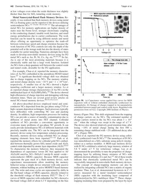
Figure 58. (a) Capacitance versus applied bias curves <strong>for</strong> MOS<br />
capacitors with or without embedded chemically synthesized Au<br />
nanoparticles. (b) Storage <strong>of</strong> charges trapped in Au nanoparticles<br />
embedded between tunnel and control oxide layers. Reprinted with<br />
permission from ref 622. Copyright 2006 Institute <strong>of</strong> Physics.<br />
history (Figure 58a). This shift originated from the trapping<br />
<strong>of</strong> charge carriers on Au NCs. The estimated number <strong>of</strong><br />
charge carriers stored in the Au NCs was about 3 × 10 11<br />
cm -2 when the voltage was swept in the range <strong>of</strong> (7 V.<br />
The device also showed relatively good retention time, after<br />
losing ∼18% <strong>of</strong> initial charge during the first 500 s,<br />
remaining charge stabilized with ∼2% additional decay after<br />
10 4 s (Figure 58b).<br />
Choi et al. reported the FG memory device using colloidally<br />
synthesized 4 nm Pt NCs. 624 The monolayer <strong>of</strong> Pt NCs<br />
was immobilized on a SiO2 substrate using poly(4-vinylpyridine)<br />
as a surface modifier. A MOS-type memory device<br />
with Pt NCs exhibited a relatively large memory window <strong>of</strong><br />
5.8 V under (7 V <strong>for</strong> write/erase voltage. Lee et al.<br />
demonstrated the possibility to tune the properties <strong>of</strong> chargetrapping<br />
layer by utilizing binary mixtures <strong>of</strong> NCs with<br />
different electron affinities (Co and Au). 625 All <strong>of</strong> these results<br />
indicate that chemically synthesized metal NCs can be<br />
successfully integrated in nonvolatile flash memory devices.<br />
The concept <strong>of</strong> charge-trapping memory can also be<br />
realized by integrating colloidal NCs into a matrix <strong>of</strong> organic<br />
insulator. Thus, Lee et al. demonstrated hysteresis in C-V<br />
curves measured <strong>for</strong> a metal-insulator-semiconductor<br />
(MIS) capacitor with the insulating layer composed <strong>of</strong><br />
polyelectrolyte/Au NCs multilayer films. 619 These chargetrapping<br />
insulating films were prepared by the layer-by-layer


