

Prospects of Colloidal Nanocrystals for Electronic - Computer Science
Prospects of Colloidal Nanocrystals for Electronic - Computer Science
Prospects of Colloidal Nanocrystals for Electronic - Computer Science

You also want an ePaper? Increase the reach of your titles
YUMPU automatically turns print PDFs into web optimized ePapers that Google loves.
<strong>Colloidal</strong> <strong>Nanocrystals</strong> in <strong>Electronic</strong> Applications Chemical Reviews, 2010, Vol. 110, No. 1 413<br />
Comparing the work function (�) <strong>of</strong> the metal electrode<br />
with energy levels <strong>of</strong> a NC can help in determining whether<br />
efficient charge injection is possible and whether high or low<br />
contact resistance is to be expected. The efficiency <strong>of</strong><br />
injection or extraction <strong>of</strong> carriers depends on the energy<br />
barriers that <strong>for</strong>m at the electrode/NC interface due to the<br />
difference in the work functions <strong>of</strong> contact material and the<br />
lowest unoccupied (<strong>for</strong> electron conductors) or highest<br />
occupied (<strong>for</strong> hole conductors) state <strong>of</strong> the NCs. A<br />
metal-semiconductor junction <strong>for</strong>ms an ohmic contact (i.e.,<br />
a contact with voltage independent resistance) if the Schottky<br />
barrier height, φB, is zero or negative. In such case, the<br />
carriers are free to flow in or out <strong>of</strong> the semiconductor so<br />
that there is a minimal resistance across the contact. A good<br />
ohmic contact is expected when the work function <strong>of</strong> the<br />
injecting metal is close to the highest occupied or lowest<br />
unoccupied states <strong>of</strong> the NCs. 360 In other words, <strong>for</strong> n-type<br />
material, the work function <strong>of</strong> the metal must be close to or<br />
smaller than the electron affinity <strong>of</strong> the semiconductor. The<br />
p-type semiconductor requires that the work function <strong>of</strong> the<br />
metal must be close to or larger than the sum <strong>of</strong> the electron<br />
affinity and the band gap energy. If these conditions are not<br />
satisfied, a potential barrier is <strong>for</strong>med, leading to poor charge<br />
injection and nonohmic contacts. High nonohmic contact<br />
resistance typically manifests itself in the transport measurements<br />
through I-V curves with suppressed current at low<br />
bias followed by superlinear increase <strong>of</strong> current at large<br />
applied voltages. High potential barriers at the metalsemiconductor<br />
interface combined with low semiconductor<br />
doping levels lead to <strong>for</strong>mation <strong>of</strong> blocking contacts, that<br />
is, the contacts that cannot inject charge carriers into<br />
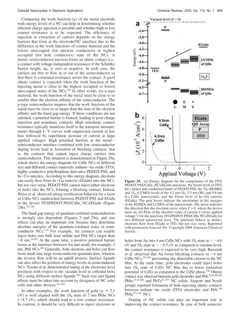
semiconductor. This situation is demonstrated in Figure 29a,<br />
which shows the energy diagram <strong>for</strong> CdSe NCs <strong>of</strong> different<br />
size and different contact materials: indium-tin oxide (ITO),<br />
highly conductive polythiophene derivative PEDOT:PSS, and<br />
In-Ca eutectics. According to this energy diagram, electrons<br />
can easily flow from In-Ga eutectic (EGaIn) into the NCs,<br />
but not vice versa. PEDOT:PSS cannot inject either electrons<br />
or holes into the NCs, <strong>for</strong>ming a blocking contact. Indeed,<br />
Weiss et al. observed strong rectification behavior <strong>for</strong> a layer<br />
<strong>of</strong> CdSe NCs sandwiched between PEDOT:PSS and EGaIn<br />
in the device ITO/PEDOT:PSS/CdSe_NCs/EGaIn (Figure<br />
29b). 361,362<br />
The band gap energy <strong>of</strong> quantum confined semiconductors<br />
is strongly size dependent (Figures 3 and 29a), and size<br />
effects can play an important role because they determine<br />
absolute energies <strong>of</strong> the quantum-confined states in semiconductor<br />
NCs. 3,39 For example, Au contacts can readily<br />
inject holes into bulk lead sulfide and PbS NCs larger than<br />
∼6 nm. 24,265 At the same time, a positive potential barrier<br />
<strong>for</strong>ms at the interface between Au and small, <strong>for</strong> example, 2<br />
nm, PbS NCs. 363 Generally, both electrons and holes can flow<br />
from small into large semiconductor quantum dots, whereas<br />
the reverse flow will be an uphill process. Surface ligands<br />
can also affect the position <strong>of</strong> energy levels in semiconductor<br />
NCs. Tessler et al. demonstrated tuning <strong>of</strong> the electronic level<br />
positions with respect to the vacuum level in colloidal InAs<br />
NCs using different surface ligands. 364 Such size and ligand<br />
effects must be taken into account by designers <strong>of</strong> NC solar<br />
cells and other devices. 361,362<br />
In other examples, the work function <strong>of</strong> gold (� ) 5.1<br />
eV) is well aligned with the 1Sh state <strong>of</strong> 7 nm PbSe NCs<br />
(∼4.7 eV), which should lead to a low contact resistance.<br />
In contrast, it should be very difficult to inject electrons or<br />
Figure 29. (a) Energy diagram <strong>for</strong> the components <strong>of</strong> the ITO/<br />
PEDOT:PSS/CdSe_NCs/EGaIn junctions: the Fermi level <strong>of</strong> ITO,<br />
the valence and conduction bands <strong>of</strong> PEDOT:PSS, the 1Sh (HOMO)<br />
and 1Se (LUMO) levels <strong>of</strong> the 4.2 nm (S), 5.3 nm (M), and 9.8 nm<br />
(L) CdSe nanocrystals, and the Fermi level <strong>of</strong> In-Ga eutectic<br />
(EGaIn). The gray boxes indicate the uncertainty in the energies<br />
<strong>of</strong> the HOMOs and LUMOs <strong>of</strong> the nanocrystals. The arrow indicates<br />
the direction that the electrons move when V > 0, where the device<br />
turns on. (b) Plots <strong>of</strong> the absolute value <strong>of</strong> current J versus applied<br />
voltage V <strong>for</strong> the junctions ITO/PEDOT:PSS/CdSe NCs/EGaIn <strong>for</strong><br />
two different nanocrystal sizes. The junctions behave as diodes:<br />
electrons flow from EGaIn to ITO, but not vice versa. Reprinted<br />
with permission from ref 361. Copyright 2008 American Chemical<br />
Society.<br />
holes from Au into 4 nm CdSe NCs with 1Se state at ∼ -4.6<br />
eV and 1Sh state at ∼ -6.5 eV as compared to vacuum level;<br />
the contact resistance is expected to be very high. Bawendi<br />
et al. observed that Au <strong>for</strong>ms blocking contacts to ∼4 nm<br />
CdSe NCs, 263,269 preventing any detectable current in the NC<br />
film. At the same time, gold electrodes could inject holes<br />
into 1Sh state <strong>of</strong> CdTe NC film due to lower ionization<br />
potential <strong>of</strong> CdTe as compared to the CdSe phase. 296 Ohmic<br />
contact was observed between gold electrodes and PbS, 22,24,265,365<br />
PbSe, 23,25,366 and PbTe 87,357 NC solids. Sargent and Nozik<br />
groups reported <strong>for</strong>mation <strong>of</strong> hole-injecting ohmic contacts<br />
between indium-tin oxide (ITO) electrodes and PbS, 365<br />
PbSe 271,367 NCs.<br />
Doping <strong>of</strong> NC solids can play an important role in<br />
improving the contact resistance. In case <strong>of</strong> bulk semicon-


