

Prospects of Colloidal Nanocrystals for Electronic - Computer Science
Prospects of Colloidal Nanocrystals for Electronic - Computer Science
Prospects of Colloidal Nanocrystals for Electronic - Computer Science

You also want an ePaper? Increase the reach of your titles
YUMPU automatically turns print PDFs into web optimized ePapers that Google loves.
<strong>Colloidal</strong> <strong>Nanocrystals</strong> in <strong>Electronic</strong> Applications Chemical Reviews, 2010, Vol. 110, No. 1 443<br />
deposition process. The optimum per<strong>for</strong>mance (memory<br />
window <strong>of</strong> ∼1.8 V) was observed <strong>for</strong> a device with three<br />
polyelectrolyte/Au_NC bilayers and a 1.4 nm thick HfO2<br />
tunneling oxide layer. Li et al. reported charge trapping<br />
leading to hysteretic C-V curves and electrical bistability<br />
<strong>for</strong> CdSe/ZnS core-shell NCs embedded in MEH-PPV 617<br />
or C60 fullerene 618 matrices. 615,616 The authors explained<br />
observed shifts in flat-band voltage by charge trapping in<br />
CdSe/ZnS NCs.<br />
Current literature demonstrates encouraging pro<strong>of</strong>-<strong>of</strong>principle<br />
demonstrations <strong>of</strong> NC-based memory devices. The<br />
further progress in this field might be accelerated by synthetic<br />
engineering <strong>of</strong> NCs. For example, a thin uni<strong>for</strong>m layer <strong>of</strong><br />
insulating oxide (SiO2, TiO2, etc.) can be grown on top <strong>of</strong><br />
Au NCs. 626,627 Such Au/SiO2 core-shell NCs look like<br />
perfect candidates <strong>for</strong> FG memory applications because they<br />
include both FG and tunnel oxide cointegrated together in<br />
the <strong>for</strong>m <strong>of</strong> solution processed units with precisely tunable<br />
size <strong>of</strong> Au core and thickness <strong>of</strong> SiO2 shell.<br />
7.5.2. Resistance-Change Memory Devices<br />
Devices incorporating switchable resistive materials are<br />
generically classified as resistive random access memory,<br />
or RRAM. The appeal <strong>of</strong> RRAM is that each element is a<br />
two-terminal device: switching between high and low<br />
resistance is achieved by means <strong>of</strong> an appropriate electrical<br />
pulse, and the read-out process consists <strong>of</strong> applying a lower<br />
voltage to probe the state <strong>of</strong> the resistance. This type <strong>of</strong><br />
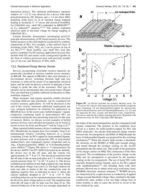
element can be incorporated into cross-point arrays (Figure<br />
59a), provided that it exhibits sufficient rectification or other<br />
nonlinear response. 570<br />
Many inorganic and organic materials exhibit electrical<br />
switching behavior and, potentially, can be considered <strong>for</strong><br />
resistive memory applications. As will be discussed at the<br />
end <strong>of</strong> this section, numerous additional requirements put<br />
very stringent limitations on materials <strong>for</strong> application in<br />
RRAM devices. In the recent years, hybrid inorganic-organic<br />
composites containing metal or semiconductor NCs are<br />
considered among the most promising materials <strong>for</strong> this type<br />
<strong>of</strong> memory. Below, we discuss several examples <strong>of</strong> hybrid<br />
memory devices; more detailed in<strong>for</strong>mation can be found in<br />
recent reviews by Scott and Bozano 570 and by Yang et al. 629<br />
Many reported hybrid memory devices combined inorganic<br />
NCs blended into an organic host. For example, Yang et al.<br />
demonstrated resistive switching behavior in a system<br />
containing 2.8 nm Au NCs capped by dodecanethiol ligands,<br />
an inert polymer such as polystyrene (PS) or poly(methyl<br />
methacrylate), and conjugated organic compound such as<br />
Alq3, 8-hydroxyquinoline (8HQ), or 9,10-dimethylanthracence<br />
(DMA). 629 Figure 59b shows I-V characteristics <strong>for</strong><br />
the device Al/(PS+Au-DT+DMA)/Al tested in air. Initially,<br />
the device was in the <strong>of</strong>f state, and the current was<br />
approximately 10 -10 A at 1 V. The electrical transition from<br />
the <strong>of</strong>f state to the on state took place at 6.1 V with an abrupt<br />
current increase from 10 -10 to 10 -6 A (curve 1). The device<br />
exhibited good stability in this high conductivity state during<br />
the subsequent voltage scan (curve 2). The high conductivity<br />
state was able to return to the low conductivity state by<br />
applying negative bias as indicated in curve 3, where the<br />
current suddenly dropped to 10 -10 A at -2.9 V. This<br />
switching behavior can be repeated numerous times and can<br />
be driven by short voltage pulses as well. The transition time<br />
from the <strong>of</strong>f state to the on state was less than 25 ns. The<br />
electrical behavior <strong>of</strong> the device was strongly dependent on<br />
Figure 59. (a) Device structure <strong>for</strong> resistive memory array. (b)<br />
I-V curves <strong>for</strong> a device Al/(composite layer)/Al with the composite<br />
layer containing 2.8 nm dodecanethiol-capped Au nanocrystals<br />
mixed with polystyrene and 9,10-dimethylanthracence. (1), (2), and<br />
(3) represent the first, second, and third bias scans, respectively.<br />
The arrows indicate the voltage-scanning directions. Reprinted with<br />
permission from ref 628. Copyright 2005 Springer.<br />
the nature <strong>of</strong> the metal nanoparticles and the conjugated small<br />
organic compound. The polymer in the composite layer<br />
served as a matrix <strong>for</strong> dodecanethiol-capped Au NCs and<br />
DMA molecules. An electric-field-induced charge transfer<br />
between the Au nanoparticle and DMA <strong>of</strong> 8HQ through the<br />
layer <strong>of</strong> dodecanethiol ligands was proposed <strong>for</strong> the switching<br />
mechanism. 629 When the electric field reaches a threshold,<br />
the electrons on the HOMO <strong>of</strong> 8HQ gain enough energy<br />
and tunnel through the insulator coating on the Au-DT<br />
nanoparticle into the metal core. This results in the generation<br />
<strong>of</strong> the charge carriers on 8HQ. The conductance <strong>of</strong> the films<br />
increased. The recombination <strong>of</strong> the positive charge on the<br />
8HQ and Au nanoparticle is prevented by the insulator<br />
coating on the Au nanoparticle. The use <strong>of</strong> metal NCs with<br />
specially designed surface ligands, such as Au NCs capped<br />
with naphthalenethiol, 630 and blending them with inert<br />
polymer allowed one to obtain write-once-read-many times<br />
(WORM) electronic memory elements. 570 WORM devices<br />
are characterized by a rapid increase in conductivity if applied<br />
voltage exceeds threshold voltage. Once switched to the highconductivity<br />
state, neither a low nor high voltage bias <strong>of</strong><br />
either polarity is able to cause the device to revert to the<br />
low-conductivity state.


