

Prospects of Colloidal Nanocrystals for Electronic - Computer Science
Prospects of Colloidal Nanocrystals for Electronic - Computer Science
Prospects of Colloidal Nanocrystals for Electronic - Computer Science

You also want an ePaper? Increase the reach of your titles
YUMPU automatically turns print PDFs into web optimized ePapers that Google loves.
<strong>Colloidal</strong> <strong>Nanocrystals</strong> in <strong>Electronic</strong> Applications Chemical Reviews, 2010, Vol. 110, No. 1 417<br />
Table 2. Reported Electron and Hole Mobilities <strong>for</strong> Various NC Films a<br />
material<br />
ligand/sample<br />
treatment particle size (nm)<br />
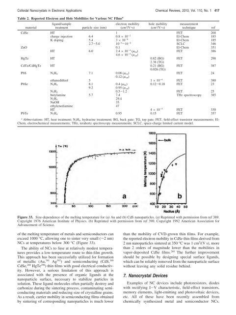
<strong>of</strong> the melting temperature <strong>of</strong> metals and semiconductors can<br />
exceed 1000 °C, allowing one to sinter very small (∼2 nm)<br />
NCs at temperatures below 300 °C (Figure 33).<br />
The ability <strong>of</strong> NCs to fuse at relatively modest temperatures<br />
provides a low-temperature route to thin-film growth.<br />
This approach has been successfully utilized <strong>for</strong> <strong>for</strong>mation<br />
<strong>of</strong> metallic (Au, 391 Ag 392 ) and semiconducting (CdS, 389<br />
CdSe, 268 HgTe 298 ) thin films with good electrical conductivity.<br />
However, a serious limitation <strong>of</strong> this approach is<br />
associated with the presence <strong>of</strong> organic ligands at the<br />
nanoparticle surface, necessary to stabilize particles in<br />
solution. These ligand molecules <strong>of</strong>ten partially destroy and<br />
carbonize during the sintering process, contaminating semiconducting<br />
materials and reducing size <strong>of</strong> crystalline grains.<br />
As a result, carrier mobility in semiconducting films obtained<br />
by sintering <strong>of</strong> corresponding nanoparticles is much lower<br />
electron mobility<br />
(cm 2 /V · s)<br />
hole mobility<br />
(cm 2 /V · s)<br />
than the mobility <strong>of</strong> CVD-grown thin films. For example,<br />
the reported electron mobility in CdSe thin films derived from<br />
2 nm nanoparticles sintered at 350 °Cwas1cm 2 /(V s), more<br />
than 2 orders <strong>of</strong> magnitude lower than the mobilities in<br />
vapor-deposited CdSe films. 268 The further improvement<br />
should be possible by designing special surface ligands,<br />
which can be reliably removed from the nanoparticle surface<br />
without leaving any solid residue behind.<br />
7. Nanocrystal Devices<br />
measurement<br />
technique ref<br />
CdSe HT 1 FET 268<br />
charge injection 6.4 0.8 × 10⁻² El-Chem 185<br />
K doping 5.4 3 × 10⁻⁶ El-Chem 185<br />
2.7-5.0 10-4-10-6 SCLC 346<br />
ZnO 0.1 El-Chem 351<br />
HT 6.0 2.4 × 10⁻⁴ (µlin)<br />
4.6 × 10<br />
FET 386<br />
-4 HgTe HT<br />
(µsat)<br />
0.82 (BG)<br />
2.38 (TG)<br />
FET 298<br />
CdTe/CdHgTe HT 0.21 (BG)<br />
0.026 (TG)<br />
FET 387<br />
PbS N2H4<br />
ethanedithiol<br />
7.1<br />
5<br />
0.08 (µlin)<br />
0.12 (µsat)<br />
1 × 10<br />
FET 24<br />
-4 FET 380<br />
PbSe N2H4<br />
N2H4<br />
butylamine<br />
8.1<br />
9.2<br />
5.7<br />
0.4 (µlin)<br />
0.95 (µsat)<br />
0.5-1.2<br />
7.4<br />
0.12-0.18 FET<br />
FET<br />
THz spectroscopy<br />
23<br />
25<br />
385<br />
N2H4<br />
29.4<br />
NaOH 35<br />
ethylenediamine 47<br />
HT 4 × 10 -5 FET 330<br />
PbTe N2H4 0.95 0.15 FET 357<br />
a Abbreviations: HT, heat treatment; N2H4, hydrazine treatement; BG, back gate; TG, top gate; FET, field-effect transistor measurements; El-<br />
Chem, electrochemical measurements; THz, terahertz spectroscopy measurements; SCLC, space-charge limited current model.<br />
Figure 33. Size-dependence <strong>of</strong> the melting temperature <strong>for</strong> (a) Au and (b) CdS nanoparticles. (a) Reprinted with permission from ref 389.<br />
Copyright 1976 American Institute <strong>of</strong> Physics. (b) Reprinted with permission from ref 390. Copyright 1992 American Association <strong>for</strong><br />
Advancement <strong>of</strong> <strong>Science</strong>.<br />
Examples <strong>of</strong> NC devices include photoresistors, diodes<br />
with rectifying I-V characteristic, field-effect transistors,<br />
memory elements, light-emitting and photovoltaic devices,<br />
etc. All <strong>of</strong> these have been recently assembled from<br />
chemically synthesized metal and semiconductor NCs.


