UNIVERSIT . . AT BONN Physikalisches Institut - Prof. Dr. Norbert ...
UNIVERSIT . . AT BONN Physikalisches Institut - Prof. Dr. Norbert ...
UNIVERSIT . . AT BONN Physikalisches Institut - Prof. Dr. Norbert ...

You also want an ePaper? Increase the reach of your titles
YUMPU automatically turns print PDFs into web optimized ePapers that Google loves.
2.4. Signal formation in direct converting pixel detectors 13<br />
In most cases the upper limit of the charge collection time for a detector of thickness D<br />
at a bias V can be estimated by the following formula.<br />
t e/h = D2<br />
µ e/h · V<br />
(2.13)<br />
The formula neglects sensor effects like the build-up of space charge, which can cause<br />
large deviations of the electric field from the externally applied one. Still, typical charge<br />
collection times in thin Si detectors (300 µm at 100 V) are on the order of 3 ns for electrons<br />
and 9 ns for holes. Thicker CdZnTe sensors typically have transit times on the order of<br />
several dozen nanoseconds.<br />
Parallel plate detector<br />
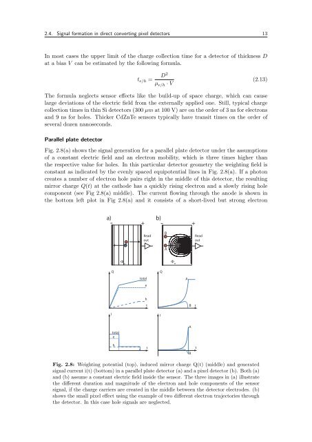
Fig. 2.8(a) shows the signal generation for a parallel plate detector under the assumptions<br />
of a constant electric field and an electron mobility, which is three times higher than<br />
the respective value for holes. In this particular detector geometry the weighting field is<br />
constant as indicated by the evenly spaced equipotential lines in Fig. 2.8(a). If a photon<br />
creates a number of electron hole pairs right in the middle of this detector, the resulting<br />
mirror charge Q(t) at the cathode has a quickly rising electron and a slowly rising hole<br />
component (see Fig 2.8(a) middle). The current flowing through the anode is shown in<br />
the bottom left plot in Fig 2.8(a) and it consists of a short-lived but strong electron<br />
a) b)<br />
+ +<br />
-<br />
I<br />
Q<br />
total<br />
e<br />
h<br />
Φ w<br />
-<br />
+<br />
Read<br />
out<br />
total<br />
e<br />
h<br />
t<br />
t<br />
Fig. 2.8: Weighting potential (top), induced mirror charge Q(t) (middle) and generated<br />
signal current i(t) (bottom) in a parallel plate detector (a) and a pixel detector (b). Both (a)<br />
and (b) assume a constant electric field inside the sensor. The three images in (a) illustrate<br />
the different duration and magnitude of the electron and hole components of the sensor<br />
signal, if the charge carriers are created in the middle between the detector electrodes. (b)<br />
shows the small pixel effect using the example of two different electron trajectories through<br />
the detector. In this case hole signals are neglected.<br />
-<br />
Q<br />
I<br />
B<br />
-<br />
-<br />
A<br />
Φ w<br />
A<br />
B<br />
A<br />
B<br />
Read<br />
out<br />
t<br />
t