UNIVERSIT . . AT BONN Physikalisches Institut - Prof. Dr. Norbert ...
UNIVERSIT . . AT BONN Physikalisches Institut - Prof. Dr. Norbert ...
UNIVERSIT . . AT BONN Physikalisches Institut - Prof. Dr. Norbert ...

You also want an ePaper? Increase the reach of your titles
YUMPU automatically turns print PDFs into web optimized ePapers that Google loves.
3.3. CIX 0.2 pixel cell concept 37<br />
Current [nA]<br />
14<br />
12<br />
10<br />
8<br />
6<br />
4<br />
2<br />
0<br />
0 100 200 300 400 500 600 700 800<br />
Time [s]<br />
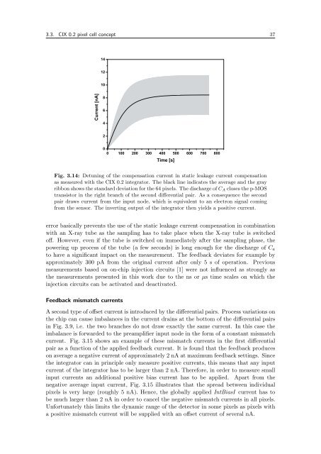
Fig. 3.14: Detuning of the compensation current in static leakage current compensation<br />
as measured with the CIX 0.2 integrator. The black line indicates the average and the gray<br />
ribbon shows the standard deviation for the 64 pixels. The discharge of CA closes the p-MOS<br />
transistor in the right branch of the second differential pair. As a consequence the second<br />
pair draws current from the input node, which is equivalent to an electron signal coming<br />
from the sensor. The inverting output of the integrator then yields a positive current.<br />
error basically prevents the use of the static leakage current compensation in combination<br />
with an X-ray tube as the sampling has to take place when the X-ray tube is switched<br />
off. However, even if the tube is switched on immediately after the sampling phase, the<br />
powering up process of the tube (a few seconds) is long enough for the discharge of Ca<br />
to have a significant impact on the measurement. The feedback deviates for example by<br />
approximately 300 pA from the original current after only 5 s of operation. Previous<br />
measurements based on on-chip injection circuits [1] were not influenced as strongly as<br />
the measurements presented in this work due to the ns or µs time scales on which the<br />
injection circuits can be activated and deactivated.<br />
Feedback mismatch currents<br />
A second type of offset current is introduced by the differential pairs. Process variations on<br />
the chip can cause imbalances in the current drains at the bottom of the differential pairs<br />
in Fig. 3.9, i.e. the two branches do not draw exactly the same current. In this case the<br />
imbalance is forwarded to the preamplifier input node in the form of a constant mismatch<br />
current. Fig. 3.15 shows an example of these mismatch currents in the first differential<br />
pair as a function of the applied feedback current. It is found that the feedback produces<br />
on average a negative current of approximately 2 nA at maximum feedback settings. Since<br />
the integrator can in principle only measure positive currents, this means that any input<br />
current of the integrator has to be larger than 2 nA. Therefore, in order to measure small<br />
input currents an additional positive bias current has to be applied. Apart from the<br />
negative average input current, Fig. 3.15 illustrates that the spread between individual<br />
pixels is very large (roughly 5 nA). Hence, the globally applied IntBiasI current has to<br />
be much larger than 2 nA in order to cancel the negative mismatch currents in all pixels.<br />
Unfortunately this limits the dynamic range of the detector in some pixels as pixels with<br />
a positive mismatch current will be supplied with an offset current of several nA.