UNIVERSIT . . AT BONN Physikalisches Institut - Prof. Dr. Norbert ...
UNIVERSIT . . AT BONN Physikalisches Institut - Prof. Dr. Norbert ...
UNIVERSIT . . AT BONN Physikalisches Institut - Prof. Dr. Norbert ...

You also want an ePaper? Increase the reach of your titles
YUMPU automatically turns print PDFs into web optimized ePapers that Google loves.
2.5. Direct converting sensor materials 15<br />
2.5 Direct converting sensor materials<br />
The selection of the direct converting sensor material plays an important role on the<br />
detector performance. Therefore this section will introduce three different sensor materials,<br />
which were used in this work. A special focus will be placed on the discussion of material<br />
related effects.<br />
2.5.1 Silicon<br />
Silicon is a widely used and well understood elementary semiconductor material. This<br />
and the lack of unwanted material effects make it a very good reference for the testing of<br />
hybrid pixel detector concepts.<br />
Concerning its physical properties, Si is a tetravalent metalloid with an atomic number of<br />
14, i.e. it is situated in the carbon group of the periodic table of elements. In its crystalline<br />
form Si is arranged in a face-centered cubic lattice with the base � (0, 0, 0), ( 1 /4, 1 /4, 1 /4) � .<br />
This structure is also called a diamond lattice. The relevant material properties of Si are<br />
given in Tab. 2.4. At room temperature the free charge carrier density in high purity<br />
Si is approximately 10 10 cm 3 . Compared to the other sensor materials in Tab. 2.4 this<br />
constitutes a relatively low resistance, which is also the reason why Si sensors have to be<br />
doped. In the doping process elements with three (p-dopant e.g. In) and five (n-dopant<br />
e.g. As) valence electrons are implanted into the Si crystal, resulting in additional acceptor<br />
(p-dopant) and donator (n-dopant) energy levels in the band gap. The combination of<br />
such p- and n-doped zones then establishes a p-n junction whose schematic representation<br />
is shown in Fig. 2.9. The major feature of this junction is the depletion zone, which<br />
is created by the diffusion of majority carriers from one zone into the oppositely doped<br />
region. In this context, the term majority carriers refers to electrons in the n-doped zone<br />
and holes in the p-doped zone. The diffusion of the charge carriers causes the build-up<br />
of a positive space charge inside the n-type Si and a negative space charge in the p-type<br />
section. This introduces an electric field, which counteracts the diffusion process and thus<br />
causes a thermal equilibrium across the junction. Fig. 2.9(b) gives a schematic view of the<br />
space charge distribution with NA (p-type) and ND (n-type) describing the acceptor and<br />
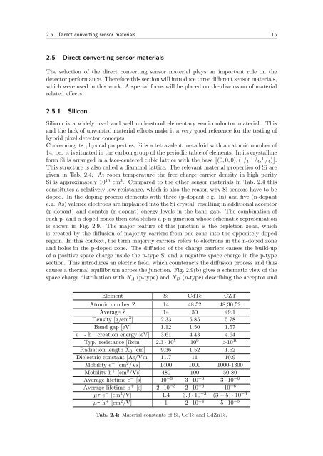
Element Si CdTe CZT<br />
Atomic number Z 14 48,52 48,30,52<br />
Average Z 14 50 49.1<br />
Density [g/cm 3 ] 2.33 5.85 5.78<br />
Band gap [eV] 1.12 1.50 1.57<br />
e − - h + creation energy [eV] 3.61 4.43 4.64<br />
Typ. resistance [Ωcm] 2.3 · 10 5 10 9 >10 10<br />
Radiation length X0 [cm] 9.36 1.52 1.52<br />
Dielectric constant [As/Vm] 11.7 11 10.9<br />
Mobility e − [cm 2 /Vs] 1400 1000 1000-1300<br />
Mobility h + [cm 2 /Vs] 480 100 50-80<br />
Average lifetime e − [s] 10 −3 3 · 10 −6 3 · 10 −6<br />
Average lifetime h + [s] 2 · 10 −3 2 · 10 −6 10 −6<br />
µτ e − [cm 2 /V] 1.4 3.3 · 10 −3 (3 − 5) · 10 −3<br />
µτ h + [cm 2 /V] 1 2 · 10 −4 5 · 10 −5<br />
Tab. 2.4: Material constants of Si, CdTe and CdZnTe.