UNIVERSIT . . AT BONN Physikalisches Institut - Prof. Dr. Norbert ...
UNIVERSIT . . AT BONN Physikalisches Institut - Prof. Dr. Norbert ...
UNIVERSIT . . AT BONN Physikalisches Institut - Prof. Dr. Norbert ...

You also want an ePaper? Increase the reach of your titles
YUMPU automatically turns print PDFs into web optimized ePapers that Google loves.
40 3. CIX 0.2 detector<br />
a)<br />
0um 1000um 2000um 3000um<br />
4000um 5000um<br />
0um<br />
1000um 2000um 3000um 0um<br />
b) c)<br />
0um 1000um 2000um 3000um<br />
4000um 5000um<br />
1000um 2000um 3000um<br />
0um 1000um 2000um 3000um<br />
4000um 5000um<br />
0um<br />
1000um 2000um 3000um<br />
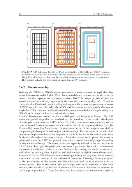
Fig. 3.17: CIX 0.2 sensor layouts. a) Pixel metallization of the CdTe and CdZnTe sensors.<br />
b) Pixel-side layout of the Si sensors. The red circles are the openings in the passivation for<br />
the gold stud bumps. c): Backside layout of the Si sensors with multi-guard ring structure.<br />
Red squares indicate the passivation openings for the HV contacts.<br />
3.4.2 Module assembly<br />
Working with CdTe and CdZnTe sensors places several constraints on the applicable chipsensor<br />
interconnect technologies. First, both materials are temperature sensitive to the<br />
extent that the exposure to temperatures above 150 ◦ C for longer periods of time (><br />
several minutes) can already significantly decrease the material quality [52]. Therefore<br />
conventional solder-based bump bonding techniques with process temperatures in excess<br />
of 250 ◦ C are ruled out. Secondly, the ASICs and the sensors were shipped in the form of<br />
single dies. This constraint makes the use of low temperature Indium bump bonding very<br />
difficult as In bump bonding is a wafer-scale process.<br />
A suited interconnect method is the so-called gold stud bumping technique. Fig. 3.18<br />
shows the general steps that are involved in this procedure. It starts with the deposit<br />
of small gold studs onto the ASIC surface. Typically these studs have diameters on the<br />
order of several dozen micrometers with a small section of the original gold wire (typ. 10-<br />
20 µm wide) protruding from the top. In some cases the top of the bumps is smoothed by<br />
compressing the bump with a flat object (called coining). The placement of the individual<br />
bumps can be performed on either single die or whole wafers but in the case of wafer scale<br />
fabrication throughput becomes an issue. After the bumps are in place, the sensor is<br />
positioned above the ASIC and pressed down with a certain force (flip-chip), depending<br />
on the number of bumps. The forces, which are typically utilized, range on the order of<br />
0.2 N/bump. The tip of the gold studs then forms a permanent bond with the surface of<br />
the sensor metallization, which is further facilitated by heating the whole module up to<br />
well below the melting point of gold but still high enough to slightly soften the material.<br />
However, CdTe and CdZnTe complicate matters significantly not only due to their thermal<br />
constraints, but also because of their mechanical tolerances. If too high forces are applied<br />
to the metallization of the sensors, the electrodes can break or loose contact with the<br />
sensor surface. This is the reason why the bumps have to be deposited on the chips<br />
and why the additional application of ultrasonic vibrations to improve the adhesion of<br />
the bumps is prohibited. These low force and low temperature requirements make it