Datascope Passport - Mindray
Datascope Passport - Mindray
Datascope Passport - Mindray
You also want an ePaper? Increase the reach of your titles
YUMPU automatically turns print PDFs into web optimized ePapers that Google loves.
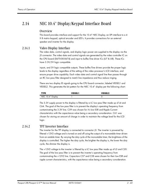
Theory of Operation NEC 10.4” Display/Keypad Interface Board<br />
2.14 NEC 10.4” Display/Keypad Interface Board<br />
Overview<br />
This board provides interface and support for the 10.4” NEC Display, an SPI interface to a 4<br />
X 8 matrix keypad, optical encoder and LED’s. It provides connections for an external<br />
speaker and inverter for the display.<br />
2.14.1 Video Display Interface<br />
The video data, control signals, and display logic power are supplied to the display via the<br />
J5 connector. The video data and control signals are generated by the video controller IC on<br />
the CPU board (0670-00-0674) and input to buffer/line driver ICs (U7 & U8). These ICs<br />
have 3.3V/5V logic compatible.<br />
inputs, and 5V logic compatible outputs. These buffer/line drivers provide the proper logic<br />
levels to the display regardless of the setting of the video processor’s LCD interface, and<br />
ensure proper drive capability. Each video data and control signal line then passes through<br />
an RC low pass filter designed to match line impedance and thus reduce ringing.<br />
There are two display ID signals going to the CPU board connector, labeled VIDSEL1 and<br />
VIDSEL2. This generates the bit pattern for the NEC 10.4” display per the following chart:<br />
TYPE VIDSEL1 VIDSEL2<br />
NEC 10.4” Display 1 0<br />
The 3.3V supply power to the display is filtered by a LC low pass filter made up of L4 and<br />
C64. The goal of the low pass filter is to prevent the display’s operating frequency from<br />
contaminating the 3.3V line. C59 was chosen for it’s low ESR and Ripple Current<br />
characteristics with the capacitance value being a secondary consideration. C61 was<br />
chosen for storing an amount of charge in order to maintain the voltage level for the LCD<br />
logic.<br />
2.14.2 TFT Inverter Interface<br />
The inverter for the TFT display is connected to connector J3. The inverter is powered by<br />
filtered +12V2 voltage and is turned on and off using the output of a monostable timer driven<br />
from an astable timer. By varying the duty cycle of the monostable timer, the brightness of the<br />
display is controlled. The higher the duty cycle, the brighter the display is, the lower the duty<br />
cycle, the dimmer the display is.<br />
The +12V2 voltage to the inverter is filtered by a LC low pass filter made up of L3 and C20.<br />
The goal of the low pass filter is to prevent the inverter’s operating frequency from<br />
contaminating the +12V2 line. Capacitors C57 and C58 were chosen for their low ESR and<br />
ripple current characteristics, with the capacitance value being a secondary consideration.<br />
<strong>Passport</strong> 2®/<strong>Passport</strong> 2 LT Service Manual 0070-10-0441 2 - 43


