- Page 1 and 2:
International Journal of computatio
- Page 3 and 4:
Meisam Mahdavi Qualification: Phd E
- Page 5 and 6:
12. 13. 14. 15. 16. 17. 18. 19. 20.
- Page 7 and 8:
15. 16. 17. 18. 19. 20. Traditional
- Page 9 and 10:
19. A Study on Security in Sensor N
- Page 11 and 12:
International Journal of Computatio
- Page 13 and 14:
Study Of The Energy Potential Of So
- Page 15 and 16:
Study Of The Energy Potential Of So
- Page 17 and 18:
Study Of The Energy Potential Of So
- Page 19 and 20:
Neural network approach to power sy
- Page 21 and 22:
Neural network approach to power sy
- Page 23 and 24:
Strength, Corrosion correlation of
- Page 25 and 26:
Strength, Corrosion correlation of
- Page 27 and 28:
Strength, Corrosion correlation of
- Page 29 and 30:
International Journal of Computatio
- Page 31 and 32:
Mutual Funds and SEBI Regulations S
- Page 33 and 34:
REFERENCES Mutual Funds and SEBI Re
- Page 35 and 36:
Integral solution of the biquadrati
- Page 37 and 38:
Integral solution of the biquadrati
- Page 39 and 40:
Experimental Studies on Effect of C
- Page 41 and 42:
Experimental Studies on Effect of C
- Page 43 and 44:
Experimental Studies on Effect of C
- Page 45 and 46:
Experimental Studies on Effect of C
- Page 47 and 48:
Simulation studies on Deep Drawing
- Page 49 and 50:
Simulation studies on Deep Drawing
- Page 51 and 52:
Radial strain Radial Strain Hoop St
- Page 53 and 54:
Simulation studies on Deep Drawing
- Page 55 and 56:
Text Extraction in Video II. MAIN C
- Page 57 and 58:
Text Extraction in Video good idea.
- Page 59 and 60:
Text Extraction in Video Fig: 5.1 T
- Page 61 and 62:
Improved Performance for “Color t
- Page 63 and 64:
Improved Performance for “Color t
- Page 65 and 66:
Improved Performance for “Color t
- Page 67 and 68:
Chain code based handwritten cursiv
- Page 69 and 70:
Chain code based handwritten cursiv
- Page 71 and 72:
Strength of Ternary Blended Cement
- Page 73 and 74:
Strength of Ternary Blended Cement
- Page 75 and 76:
International Journal of Computatio
- Page 77 and 78:
Ni-Based Cr Alloys and Grain Bounda
- Page 79 and 80:
International Journal of Computatio
- Page 81 and 82:
Comparative Study of Available Tech
- Page 83 and 84:
Comparative Study of Available Tech
- Page 85 and 86:
Analyzing massive machine data main
- Page 87 and 88:
Analyzing massive machine data main
- Page 89 and 90:
Implementation Of An Algorithmic To
- Page 91 and 92:
Implementation Of An Algorithmic To
- Page 93 and 94:
Implementation Of An Algorithmic To
- Page 95 and 96:
Implementation Of An Algorithmic To
- Page 97 and 98:
Model Order Reduction By Mixed... a
- Page 99 and 100:
Amplitude The unit time step respon
- Page 101 and 102:
Enterprise Management Information S
- Page 103 and 104:
Enterprise Management Information S
- Page 105 and 106:
A Novel Approach For Filtering Unre
- Page 107 and 108:
A Novel Approach For Filtering Unre
- Page 109 and 110:
Current Routing Strategies To Adapt
- Page 111 and 112:
Energy Based Routing Protocol for W
- Page 113 and 114:
Energy Based Routing Protocol for W
- Page 115 and 116:
Cfd Analysis of Convergent- Diverge
- Page 117 and 118:
Cfd Analysis of Convergent- Diverge
- Page 119 and 120:
Cfd Analysis of Convergent- Diverge
- Page 121 and 122:
Cfd Analysis of Convergent- Diverge
- Page 123 and 124:
Cfd Analysis of Convergent- Diverge
- Page 125 and 126:
Cfd Analysis of Convergent- Diverge
- Page 127 and 128:
Observation on the Ternary Cubic Eq
- Page 129 and 130:
(2) n n 3n n x (2 ,1) y(2 ,1) 3[
- Page 131 and 132:
Observation on the Ternary Cubic Eq
- Page 133 and 134:
Integral Solutions of the Homogeneo
- Page 135 and 136:
Integral Solutions of the Homogeneo
- Page 137 and 138:
International Journal of Computatio
- Page 139 and 140:
International Journal of Computatio
- Page 141 and 142:
International Journal of Computatio
- Page 143 and 144:
International Journal of Computatio
- Page 145 and 146:
Dividing expression (a) by (b), P =
- Page 147 and 148:
Highly Efficient Motorized…. Torq
- Page 149 and 150:
Highly Efficient Motorized…. = =
- Page 151 and 152:
International Journal of Computatio
- Page 153 and 154:
A comparative study of Broadcasting
- Page 155 and 156:
A comparative study of Broadcasting
- Page 157 and 158:
Recommendation Systems: a review Co
- Page 159 and 160:
Recommendation Systems: a review 1.
- Page 161 and 162:
Recommendation Systems: a review V.
- Page 163 and 164:
Using Fast Fourier Extraction Metho
- Page 165 and 166:
Using Fast Fourier Extraction Metho
- Page 167 and 168:
Using Fast Fourier Extraction Metho
- Page 169 and 170:
International Journal of Computatio
- Page 171 and 172:
P= Number of Poles. d) Fourth Objec
- Page 173 and 174:
Using Genetic Algorithm Minimizing
- Page 175 and 176:
Using Genetic Algorithm Minimizing
- Page 177 and 178:
Literature review: Iris Segmentatio
- Page 179 and 180:
Literature review: Iris Segmentatio
- Page 181 and 182:
Effects of Agreement on Trims on In
- Page 183 and 184:
Effects of Agreement on Trims on In
- Page 185 and 186:
Effects of Agreement on Trims on In
- Page 187 and 188:
A Novel Approach to Mine Frequent I
- Page 189 and 190:
A Novel Approach to Mine Frequent I
- Page 191 and 192:
Time(ms) A Novel Approach to Mine F
- Page 193 and 194:
International Journal of Computatio
- Page 195 and 196:
Similarly, reactions at bearings (1
- Page 197 and 198:
Modeling and Analysis of the Cranks
- Page 199 and 200:
International Journal of Computatio
- Page 201 and 202:
Efficient Model for OFDM based IEEE
- Page 203 and 204:
Efficient Model for OFDM based IEEE
- Page 205 and 206:
Efficient Model for OFDM based IEEE
- Page 207 and 208:
International Journal of Computatio
- Page 209 and 210:
Traditional Uses Of Plants By The T
- Page 211 and 212:
Traditional Uses Of Plants By The T
- Page 213 and 214:
International Journal of Computatio
- Page 215 and 216:
Content Based Video Retrieval Using
- Page 217 and 218:
Content Based Video Retrieval Using
- Page 219 and 220:
Effective and secure content retrie
- Page 221 and 222:
Effective and secure content retrie
- Page 223 and 224:
Effective and secure content retrie
- Page 225 and 226:
speed rad/sec Master-Slave Speed Co
- Page 227 and 228:
speed rad/sec speed rad/sec speed r
- Page 229 and 230:
Cd-Hmm For Normal Sinus Rhythm 1 0
- Page 231 and 232:
Cd-Hmm For Normal Sinus Rhythm III.
- Page 233 and 234:
Develop A Electricity Utility… In
- Page 235 and 236:
Develop A Electricity Utility… Ex
- Page 237 and 238:
Develop A Electricity Utility… Fi
- Page 239 and 240:
International Journal of Computatio
- Page 241 and 242:
Implementing CURE to Address Scalab
- Page 243 and 244:
Implementing CURE to Address Scalab
- Page 245 and 246:
Implementing CURE to Address Scalab
- Page 247 and 248:
Design of Uniform Fiber Bragg grati
- Page 249 and 250:
Design of Uniform Fiber Bragg grati
- Page 251 and 252:
Reflectivity (%) Reflectivity (%) D
- Page 253 and 254:
Effect of Alkaline Activator on Wor
- Page 255 and 256:
comp. strengthin Mpa Comp. strength
- Page 257 and 258:
Effect of Alkaline Activator on Wor
- Page 259 and 260:
Priority Based Service Composition
- Page 261 and 262:
Priority Based Service Composition
- Page 263 and 264:
International Journal of Computatio
- Page 265 and 266:
Formation of pseudo-random sequence
- Page 267 and 268:
Formation of pseudo-random sequence
- Page 269 and 270:
Formation of pseudo-random sequence
- Page 271 and 272:
International Journal of Computatio
- Page 273 and 274:
Block mathematical coding method of
- Page 275 and 276:
Block mathematical coding method of
- Page 277 and 278:
International Journal of Computatio
- Page 279 and 280:
Fast Encryption Algorithm for Strea
- Page 281 and 282:
International Journal of Computatio
- Page 283 and 284:
Area and Speed wise superior Vedic
- Page 285 and 286:
Area and Speed wise superior Vedic
- Page 287 and 288:
International Journal of Computatio
- Page 289 and 290:
Effect of nano-silica on properties
- Page 291 and 292:
Effect of nano-silica on properties
- Page 293 and 294:
International Journal of Computatio
- Page 295 and 296:
Load forecasting for practical powe
- Page 297 and 298:
In scalar notation, the fitted mode
- Page 299 and 300:
Mape load in MW Load forecasting fo
- Page 301 and 302: Load forecasting for practical powe
- Page 303 and 304: International Journal of Computatio
- Page 305 and 306: Efirstaid medical services for acci
- Page 307 and 308: International Journal of Computatio
- Page 309 and 310: Comparative study of capacitance of
- Page 311 and 312: Comparative study of capacitance of
- Page 313 and 314: Increasing the Comprehensibility of
- Page 315 and 316: Increasing the Comprehensibility of
- Page 317 and 318: International Journal of Computatio
- Page 319 and 320: Smart Message Communication for War
- Page 321 and 322: International Journal of Computatio
- Page 323 and 324: In Mobile Ad hoc Networks: Issues a
- Page 325 and 326: In Mobile Ad hoc Networks: Issues a
- Page 327 and 328: International Journal of Computatio
- Page 329 and 330: Comparison Of UPS Inverter Using PI
- Page 331 and 332: Comparison Of UPS Inverter Using PI
- Page 333 and 334: Comparison Of UPS Inverter Using PI
- Page 335 and 336: International Journal of Computatio
- Page 337 and 338: Ageing Behaviour of Epdm/Pvc Compos
- Page 339 and 340: Ageing Behaviour of Epdm/Pvc Compos
- Page 341 and 342: International Journal of Computatio
- Page 343 and 344: On Α Locally Finite In Ditopologic
- Page 345 and 346: International Journal of Computatio
- Page 347 and 348: A Study On Security In Sensor… IE
- Page 349 and 350: A Study On Security In Sensor… Th
- Page 351: International Journal of Computatio
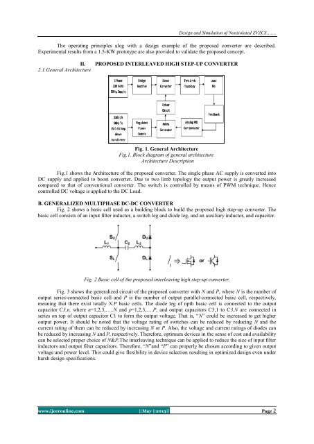
- Page 355 and 356: Design and Simulation of Nonisolate
- Page 357 and 358: Design and Simulation of Nonisolate
- Page 359 and 360: Design and Simulation of Nonisolate
- Page 361 and 362: Evaluating The Privacy Measure Of T
- Page 363 and 364: Evaluating The Privacy Measure Of T
- Page 365 and 366: Work Done On Avoidance… n New RA
- Page 367 and 368: Work Done On Avoidance… Probabili
- Page 369 and 370: Data Aggregation Protocols In Wirel
- Page 371 and 372: Data Aggregation Protocols In Wirel
- Page 373 and 374: Data Aggregation Protocols In Wirel
- Page 375 and 376: International Journal of Computatio
- Page 377 and 378: Development Of Virtual Backbone…
- Page 379 and 380: Development Of Virtual Backbone…
- Page 381 and 382: International Journal of Computatio
- Page 383 and 384: Domain Driven Data Mining: An… To
- Page 385 and 386: Domain Driven Data Mining: An… X
- Page 387 and 388: Domain Driven Data Mining: An… [5
- Page 389 and 390: The Rhythm Of Omission Of Articles
- Page 391 and 392: All of them are from Rural backgrou
- Page 393 and 394: The Rhythm Of Omission Of Articles
- Page 395 and 396: The Rhythm Of Omission Of Articles
- Page 397 and 398: The Rhythm Of Omission Of Articles
- Page 399 and 400: The Rhythm Of Omission Of Articles
- Page 401 and 402: Image Segmentation using RGB… gra
- Page 403 and 404:
Image Segmentation using RGB… and
- Page 405 and 406:
Image Segmentation using RGB… [8]
- Page 407 and 408:
Performance Comparison Of Rayleigh
- Page 409 and 410:
Performance Comparison Of Rayleigh
- Page 411 and 412:
Performance Comparison Of Rayleigh
- Page 413 and 414:
International Journal of Computatio
- Page 415 and 416:
Walking the talk in training future
- Page 417 and 418:
Walking the talk in training future
- Page 419 and 420:
Walking the talk in training future
- Page 421 and 422:
International Journal of Computatio
- Page 423 and 424:
Experimental Investigation Of Multi
- Page 425 and 426:
Experimental Investigation Of Multi
- Page 427 and 428:
Experimental Investigation Of Multi
- Page 429 and 430:
A Firm Retrieval Of Software… Cla
- Page 431 and 432:
A Firm Retrieval Of Software… hop
- Page 433 and 434:
A Firm Retrieval Of Software… tab
- Page 435 and 436:
2.1. Introduction to Service Matchi
- Page 437 and 438:
Reduced Complexity Of Service Match
- Page 439 and 440:
International Journal of Computatio
- Page 441 and 442:
Pulsed Electrodeposition Of Nano…
- Page 443 and 444:
Pulsed Electrodeposition Of Nano…