Remote Health Monitoring for Asset Management
Remote Health Monitoring for Asset Management
Remote Health Monitoring for Asset Management

Create successful ePaper yourself
Turn your PDF publications into a flip-book with our unique Google optimized e-Paper software.
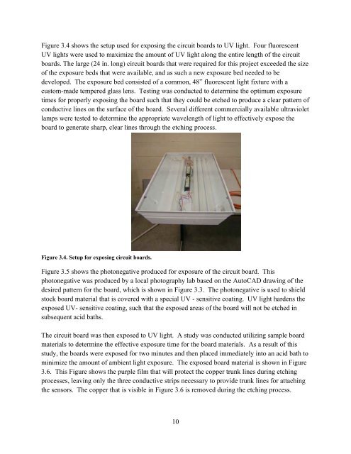
Figure 3.4 shows the setup used <strong>for</strong> exposing the circuit boards to UV light. Four fluorescent<br />
UV lights were used to maximize the amount of UV light along the entire length of the circuit<br />
boards. The large (24 in. long) circuit boards that were required <strong>for</strong> this project exceeded the size<br />
of the exposure beds that were available, and as such a new exposure bed needed to be<br />
developed. The exposure bed consisted of a common, 48” fluorescent light fixture with a<br />
custom-made tempered glass lens. Testing was conducted to determine the optimum exposure<br />
times <strong>for</strong> properly exposing the board such that they could be etched to produce a clear pattern of<br />
conductive lines on the surface of the board. Several different commercially available ultraviolet<br />
lamps were tested to determine the appropriate wavelength of light to effectively expose the<br />
board to generate sharp, clear lines through the etching process.<br />
Figure 3.4. Setup <strong>for</strong> exposing circuit boards.<br />
Figure 3.5 shows the photonegative produced <strong>for</strong> exposure of the circuit board. This<br />
photonegative was produced by a local photography lab based on the AutoCAD drawing of the<br />
desired pattern <strong>for</strong> the board, which is shown in Figure 3.3. The photonegative is used to shield<br />
stock board material that is covered with a special UV - sensitive coating. UV light hardens the<br />
exposed UV- sensitive coating, such that the exposed areas of the board will not be etched in<br />
subsequent acid baths.<br />
The circuit board was then exposed to UV light. A study was conducted utilizing sample board<br />
materials to determine the effective exposure time <strong>for</strong> the board materials. As a result of this<br />
study, the boards were exposed <strong>for</strong> two minutes and then placed immediately into an acid bath to<br />
minimize the amount of ambient light exposure. The exposed board material is shown in Figure<br />
3.6. This Figure shows the purple film that will protect the copper trunk lines during etching<br />
processes, leaving only the three conductive strips necessary to provide trunk lines <strong>for</strong> attaching<br />
the sensors. The copper that is visible in Figure 3.6 is removed during the etching process.<br />
10