- Page 4 and 5:
Chapter 1 Naked eye observations 1.
- Page 6 and 7:
A month 5 seen to rise above the ea
- Page 8 and 9:
A year 7 between south and west. An
- Page 10 and 11:
Chapter 2 Ancient world models Firs
- Page 12 and 13:
Ancient world models 11 Figure 2.1.
- Page 14 and 15:
Chapter 3 Observations made by inst
- Page 16 and 17:
Instrumentation in astronomy 15 Fig
- Page 18 and 19:
The role of the observer 17 Earth a
- Page 20 and 21:
Electromagnetic radiation 19 meteor
- Page 22 and 23:
Electromagnetic radiation 21 If, fo
- Page 24 and 25:
Electromagnetic radiation 23 device
- Page 26 and 27:
Direction of arrival of the radiati
- Page 28 and 29:
Brightness 27 Figure 5.3. The windo
- Page 30 and 31:
Brightness 29 physical conditions w
- Page 32 and 33:
Time 31 to house radio transmitters
- Page 34 and 35:
Chapter 6 The night sky 6.1 Star ma
- Page 36 and 37:
Simple observations 35 Figure 6.1.
- Page 38 and 39:
Simple observations 37 Figure 6.4.
- Page 40 and 41:
Simple observations 39 Figure 6.6.
- Page 42 and 43:
Simple observations 41 Figure 6.8.
- Page 44 and 45:
Chapter 7 The geometry of the spher
- Page 46 and 47:
Position on the Earth’s surface 4
- Page 48 and 49:
Position on the Earth’s surface 4
- Page 50 and 51:
Spherical trigonometry 51 determine
- Page 52 and 53:
Spherical trigonometry 53 Figure 7.
- Page 54 and 55:
The small spherical triangle 55 7.4
- Page 56 and 57:
Problems—Chapter 7 57 Although th
- Page 58 and 59:
Chapter 8 The celestial sphere: coo
- Page 60 and 61:
The equatorial system 61 Figure 8.2
- Page 62 and 63:
Circumpolar stars 63 Figure 8.4. A
- Page 64 and 65:
Also Hence, we have or The measurem
- Page 66 and 67:
The geocentric celestial sphere 67
- Page 68 and 69:
Transformation of one coordinate sy
- Page 70 and 71:
Right ascension 71 or cos 47 ◦ 39
- Page 72 and 73:
The Sun’s geocentric behaviour 73
- Page 74 and 75:
Sunset and sunrise 75 Figure 8.15.
- Page 76 and 77:
Megalithic man and the Sun 77 Figur
- Page 78 and 79:
The ecliptic system of coordinates
- Page 80 and 81:
Galactic coordinates 81 Table 8.1.
- Page 82 and 83:
Galactic coordinates 83 Figure 8.22
- Page 84 and 85:
Galactic coordinates 85 Figure 8.25
- Page 86 and 87:
Problems—Chapter 8 87 where ε is
- Page 88 and 89:
Sidereal time 89 Figure 9.1. The ti
- Page 90 and 91:
Sidereal time 91 Figure 9.3. An equ
- Page 92 and 93:
Mean solar time 93 Figure 9.4. Posi
- Page 94 and 95:
The relationship between mean solar
- Page 96 and 97:
The civil day and timekeeping 97 It
- Page 98 and 99:
The tropical year and the calendar
- Page 100 and 101:
The Earth’s geographical zones 10
- Page 102 and 103:
Hence, the period of the year durin
- Page 104 and 105:
Twilight 105 Figure 9.10. The heati
- Page 106 and 107:
Twilight 107 For this to happen, ZB
- Page 108 and 109:
h m s Date Approximate ZT 16 30 0 J
- Page 110 and 111:
Problems—Chapter 9 111 Date (00 h
- Page 112 and 113:
Atmospheric refraction 113 Figure 1
- Page 114 and 115:
where ZOL = r. But ZOL = ζ .AlsoAB
- Page 116 and 117:
so that we have But Hence, Similarl
- Page 118 and 119:
Now But θ is a small angle so we m
- Page 120 and 121:
Geocentric parallax 121 Figure 10.6
- Page 122 and 123:
The semi-diameter of a celestial ob
- Page 124 and 125:
Measuring distance in the Solar Sys
- Page 126 and 127:
Stellar parallax 127 Figure 10.10.
- Page 128 and 129:
Stellar parallax 129 after. The val
- Page 130 and 131:
Problems—Chapter 10 131 Recent ob
- Page 132 and 133:
Chapter 11 The reduction of positio
- Page 134 and 135:
The velocity of light 135 Table 11.
- Page 136 and 137:
The constant of aberration 137 Figu
- Page 138 and 139:
Diurnal and planetary aberration 13
- Page 140 and 141:
Precession of the equinoxes 141 Fig
- Page 142 and 143:
Effect of precession on a star’s
- Page 144 and 145:
Nutation 145 Figure 11.10. The grav
- Page 146 and 147:
The tropical and sidereal years 147
- Page 148 and 149:
Chapter 12 Geocentric planetary phe
- Page 150 and 151:
The Copernican System 151 Figure 12
- Page 152 and 153:
Planetary configurations 153 (a) V
- Page 154 and 155:
The synodic period 155 Figure 12.5.
- Page 156 and 157:
Measurement of planetary distances
- Page 158 and 159:
Stationary points 159 Figure 12.8.
- Page 160 and 161:
Stationary points 161 Using equatio
- Page 162 and 163:
The phase of a planet 163 Figure 12
- Page 164 and 165:
Problems—Chapter 12 165 with an o
- Page 166 and 167:
Planetary orbits 167 Figure 13.1. M
- Page 168 and 169:
Planetary orbits 169 If P 1 SP 2 is
- Page 170 and 171:
Newton’s law of gravitation 171 a
- Page 172 and 173:
The Principia of Isaac Newton 173 N
- Page 174 and 175:
The two-body problem 175 Figure 13.
- Page 176 and 177:
The two-body problem 177 Figure 13.
- Page 178 and 179:
The two-body problem 179 13.6.5 The
- Page 180 and 181:
The two-body problem 181 Figure 13.
- Page 182 and 183:
The astronomical unit 183 For an ex
- Page 184 and 185:
Chapter 14 Celestial mechanics: the
- Page 186 and 187:
14.3 General properties of the many
- Page 188 and 189:
Special perturbation theories 189 F
- Page 190 and 191:
Special perturbation theories 191 F
- Page 192 and 193:
14.6 Dynamics of artificial Earth s
- Page 194 and 195:
The geostationary satellite 195 in
- Page 196 and 197:
Interplanetary transfer orbits 197
- Page 198 and 199:
Then V B = V c2 − V A ,sinceV c2
- Page 200 and 201:
Interplanetary transfer orbits 201
- Page 202 and 203:
Interplanetary transfer orbits 203
- Page 204 and 205:
Problems—Chapter 14 205 (figure 1
- Page 206 and 207:
210 The radiation laws Figure 15.1.
- Page 208 and 209:
212 The radiation laws Table 15.1.
- Page 210 and 211:
214 The radiation laws Figure 15.2.
- Page 212 and 213:
216 The radiation laws In order to
- Page 214 and 215:
218 The radiation laws where σ is
- Page 216 and 217:
220 The radiation laws The brightne
- Page 218 and 219:
222 The radiation laws centrifugal
- Page 220 and 221:
224 The radiation laws Figure 15.7.
- Page 222 and 223:
226 The radiation laws is moving pa
- Page 224 and 225:
228 The radiation laws Figure 15.9.
- Page 226 and 227:
230 The radiation laws In most phys
- Page 228 and 229:
232 The radiation laws radiation ha
- Page 230 and 231:
234 The radiation laws radiation is
- Page 232 and 233:
236 The radiation laws Figure 15.14
- Page 234 and 235:
Chapter 16 The optics of telescope
- Page 236 and 237:
240 The optics of telescope collect
- Page 238 and 239:
242 The optics of telescope collect
- Page 240 and 241:
244 The optics of telescope collect
- Page 242 and 243:
246 The optics of telescope collect
- Page 244 and 245:
248 The optics of telescope collect
- Page 246 and 247: 250 The optics of telescope collect
- Page 248 and 249: 252 The optics of telescope collect
- Page 250 and 251: 254 The optics of telescope collect
- Page 252 and 253: 256 The optics of telescope collect
- Page 254 and 255: 258 The optics of telescope collect
- Page 256 and 257: 260 The optics of telescope collect
- Page 258 and 259: 262 The optics of telescope collect
- Page 260 and 261: 264 The optics of telescope collect
- Page 262 and 263: 266 The optics of telescope collect
- Page 264 and 265: 268 The optics of telescope collect
- Page 266 and 267: 270 The optics of telescope collect
- Page 268 and 269: Chapter 17 Visual use of telescopes
- Page 270 and 271: 274 Visual use of telescopes By sub
- Page 272 and 273: 276 Visual use of telescopes 17.3 M
- Page 274 and 275: 278 Visual use of telescopes By let
- Page 276 and 277: 280 Visual use of telescopes Figure
- Page 278 and 279: 282 Visual use of telescopes For sm
- Page 280 and 281: 284 Detectors for optical telescope
- Page 282 and 283: 286 Detectors for optical telescope
- Page 284 and 285: 288 Detectors for optical telescope
- Page 286 and 287: 290 Detectors for optical telescope
- Page 288 and 289: 292 Detectors for optical telescope
- Page 290 and 291: 294 Detectors for optical telescope
- Page 292 and 293: 296 Detectors for optical telescope
- Page 294 and 295: 298 Detectors for optical telescope
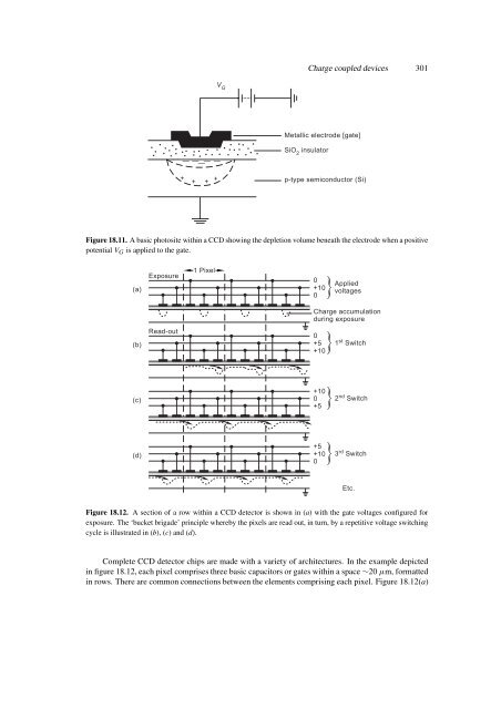
- Page 298 and 299: 302 Detectors for optical telescope
- Page 300 and 301: 304 Detectors for optical telescope
- Page 302 and 303: 306 Astronomical optical measuremen
- Page 304 and 305: 308 Astronomical optical measuremen
- Page 306 and 307: 310 Astronomical optical measuremen
- Page 308 and 309: 312 Astronomical optical measuremen
- Page 310 and 311: 314 Astronomical optical measuremen
- Page 312 and 313: 316 Astronomical optical measuremen
- Page 314 and 315: 318 Astronomical optical measuremen
- Page 316 and 317: 320 Astronomical optical measuremen
- Page 318 and 319: 322 Astronomical optical measuremen
- Page 320 and 321: 324 Astronomical optical measuremen
- Page 322 and 323: 326 Astronomical optical measuremen
- Page 324 and 325: 328 Astronomical optical measuremen
- Page 326 and 327: Chapter 20 Modern telescopes and ot
- Page 328 and 329: 332 Modern telescopes and other opt
- Page 330 and 331: 334 Modern telescopes and other opt
- Page 332 and 333: 336 Modern telescopes and other opt
- Page 334 and 335: 338 Modern telescopes and other opt
- Page 336 and 337: 340 Modern telescopes and other opt
- Page 338 and 339: 342 Modern telescopes and other opt
- Page 340 and 341: 344 Modern telescopes and other opt
- Page 342 and 343: 346 Modern telescopes and other opt
- Page 344 and 345: 348 Modern telescopes and other opt
- Page 346 and 347:
350 Modern telescopes and other opt
- Page 348 and 349:
Chapter 21 Radio telescopes 21.1 In
- Page 350 and 351:
354 Radio telescopes Figure 21.2. A
- Page 352 and 353:
356 Radio telescopes Figure 21.3. A
- Page 354 and 355:
358 Radio telescopes Figure 21.6. T
- Page 356 and 357:
360 Radio telescopes Figure 21.8. A
- Page 358 and 359:
362 Radio telescopes (a) Paraboloid
- Page 360 and 361:
364 Radio telescopes Figure 21.12.
- Page 362 and 363:
366 Radio telescopes The record fro
- Page 364 and 365:
368 Radio telescopes 2 N N Figure 2
- Page 366 and 367:
370 Radio telescopes Figure 21.19.
- Page 368 and 369:
372 Radio telescopes Figure 21.22.
- Page 370 and 371:
Chapter 22 Telescope mountings 22.1
- Page 372 and 373:
376 Telescope mountings arc and thi
- Page 374 and 375:
378 Telescope mountings Figure 22.4
- Page 376 and 377:
380 Telescope mountings The design
- Page 378 and 379:
382 High energy instruments and oth
- Page 380 and 381:
384 High energy instruments and oth
- Page 382 and 383:
386 High energy instruments and oth
- Page 384 and 385:
388 High energy instruments and oth
- Page 386 and 387:
390 High energy instruments and oth
- Page 388 and 389:
392 High energy instruments and oth
- Page 390 and 391:
394 High energy instruments and oth
- Page 392 and 393:
396 High energy instruments and oth
- Page 394 and 395:
398 High energy instruments and oth
- Page 396 and 397:
400 High energy instruments and oth
- Page 398 and 399:
404 Practical projects to give the
- Page 400 and 401:
406 Practical projects Figure 24.2.
- Page 402 and 403:
408 Practical projects measurement
- Page 404 and 405:
410 Practical projects Figure 24.5.
- Page 406 and 407:
412 Practical projects Figure 24.6.
- Page 408 and 409:
414 Practical projects Figure 24.8.
- Page 410 and 411:
416 Practical projects Summer Time
- Page 412 and 413:
418 Practical projects Figure 24.12
- Page 414 and 415:
420 Practical projects Figure 24.13
- Page 416 and 417:
422 Practical projects point was ch
- Page 418 and 419:
424 Practical projects Figure 24.16
- Page 420 and 421:
426 Practical projects N φ Earth 1
- Page 422 and 423:
428 Practical projects 24.5 Solar d
- Page 424 and 425:
430 Practical projects allows the S
- Page 426 and 427:
432 Practical projects 24.5.4 The e
- Page 428 and 429:
434 Practical projects Figure 24.22
- Page 430 and 431:
436 Practical projects Figure 24.24
- Page 432 and 433:
438 Practical projects Now in t hou
- Page 434 and 435:
440 Practical projects Table 24.2.
- Page 436 and 437:
442 Practical projects 24.7.2 The i
- Page 438 and 439:
444 Practical projects Figure 24.29
- Page 440 and 441:
446 Practical projects Figure 24.30
- Page 442 and 443:
448 Practical projects right ascens
- Page 444 and 445:
450 Practical projects amenable to
- Page 446 and 447:
452 Web sites • W 20.5—www.mrao
- Page 448 and 449:
Appendix: Astronomical and related
- Page 450 and 451:
456 Appendix: Astronomical and rela
- Page 452 and 453:
Bibliography 1 Source books The Ast
- Page 454 and 455:
Answers to problems Chapter 7 1. 32
- Page 456 and 457:
462 Answers to problems Figure A8.2
- Page 458 and 459:
464 Answers to problems Figure A10.
- Page 460 and 461:
466 Answers to problems Figure A13.
- Page 462 and 463:
468 Answers to problems 5. 1·64 6.
- Page 464 and 465:
470 Index black body radiation, 216
- Page 466 and 467:
472 Index atom, 221 line, 353 illum
- Page 468 and 469:
474 Index potential energy, 177 pow