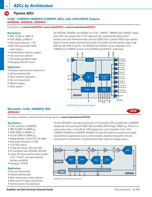
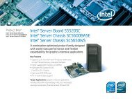
66➔ADCs by ArchitecturePipeline ADCs14-Bit, 170MSPS/190MSPS/210MSPS ADCs with LVDS/CMOS OutputsADS5545, ADS5546, ADS5547Get datasheets at: www.ti.com/ADS5546, www.ti.com/ADS5545 or www.ti.com/sc/device/ADS5547Key Features• SNR: 73.2dBc at 70MHz IF• SFDR: 84dBc at 70MHz IF• Total power disipation: 1.1W• DDR LVDS <strong>and</strong> parallel CMOSoutput options• Internal/external reference support• Clock duty cycle stabilizer• 3.3V analog <strong>and</strong> digital supply• Packaging: QFN-48 (7x7mm)Applications• Wireless communication infrastructure• Software-defined radio• Power amplifier linearization• Test <strong>and</strong> measurement• Medical imaging• Radar systemsThe ADS5545, ADS5546, <strong>and</strong> ADS5547 are 14-bit, 170MSPS, 190MSPS <strong>and</strong> 210MSPS, respectively,ADCs that operate from a 3.3V supply <strong>and</strong> offer unprecedented digital outputflexibility with fully differential double data rate (DDR) LVDS or parallel CMOS output options.Using an internal sample <strong>and</strong> hold <strong>and</strong> low jitter clock buffer, the three devices support highSNR <strong>and</strong> high SFDR at high IFs. The ADS5525 <strong>and</strong> ADS5527 are pin compatible 12-bit,170MSPS <strong>and</strong> 210MSPS versions of the ADS5545 <strong>and</strong> ADS5547, respectively.CLKPCLKMINPINMVCMSHAAVDDADS5547AGNDCLOCKGEN14-BitADCReferenceDigital Encoder<strong>and</strong>SerializerControlInterfaceDRVDDDRGNDCLKOUTPCLKOUTMD0_D1_PD0_D1_MD2_D3_PD2_D3_MD4_D5_PD4_D5_MD6_D7_PD6_D7_MD8_D9_PD8_D9_MD10_D11_PD10_D11_MD12_D13_PD12_D13_MOVRIREFSCLKSENSDATARESETOEDFSMODELVDS MODEMonolithic 12-Bit, 500MSPS ADCADS5463ADS5547 functional block diagram.Get samples, datasheets, evaluation modules <strong>and</strong> app reports at: www.ti.com/sc/device/ADS5463Key Features• 12-bit resolution at 500MSPS• SNR: 65.5dBFS at 100MHz f IN• SFDR: 80dBc at 100MHz f IN• 10.5-bit ENOB at 100MHz f IN• Analog operation: 5V <strong>and</strong> 3.3V, 3.3V digital• Total power dissipation: 2.25W• 3.3V LVDS outputs• 2.2Vpp input range; 2GHz input BW• Pin compatible with ADS5440, ADS5444• I-temp, Mil-temp enhanced plastic product(114 x 114mm 2 ), <strong>and</strong> space qualifiedpackage availability• Packaging: TQFP-80Applications• Test <strong>and</strong> measurement• Software-defined radio• Multi-channel base station receivers• Base station TX digital predistortion• Communications instrumentationThe new ADS5463 is the highest performing 12-bit monolithic ADC available with a 500MSPSsample rate while providing 65.5dBFS SNR <strong>and</strong> 80dBc SFDR through 100MHz f IN . Offered in aspace-saving 14mm x 14mm 80-pin TQFP package that is pin compatible to the 13-bit,210MSPS ADS5440 <strong>and</strong> 250MSPS ADS5444, the new ADC meets the resolution <strong>and</strong> speedrequirements for applications such as communications, amplifier linearization, test <strong>and</strong>measurement instrumentation, software-defined radio, radar <strong>and</strong> imaging systems.A1 TH1 TH2 ∑ A2 TH3 ∑ A3ReferenceTimingADC1ADS5463 functional block diagram.5DAC1ADC2Digital Error Correction5DAC2ADC3ADS54635<strong>Amplifier</strong> <strong>and</strong> <strong>Data</strong> <strong>Converter</strong> <strong>Selection</strong> <strong>Guide</strong> Texas Instruments 3Q 2007
ADCs by Architecture67Pipeline ADCs <strong>Selection</strong> <strong>Guide</strong>Pipeline ADCsSample # of Input Analog Input SupplyRes. Rate Input Voltage B<strong>and</strong>width DNL INL SNR SFDR Voltage PowerDevice (Bits) (MSPS) Channels (V) (MHz) (± LSB) (± LSB) (dB) (dB) (V) (mW) Package(s) Price *ADS5547 14 210 1 Diff 2 800 0.5 — 73.3 85 3, 3.6 1230 QFN-48 $82.50ADS5546 14 190 1 Diff 2 500 0.5 3 73.2 84 3, 3.6 1130 QFN-48 $72.50ADS5545 14 170 1 Diff 2 500 0.5 3 73.5 85 3, 3.6 1100 QFN-48 $62.50ADS5500 14 125 1 Diff 2 750 1.1 5 70.5 82 3, 3.6 780 HTQFP-64 $49.00ADS6245 14 125 2 Diff 2 500 2.5 5 73.2 83 3, 3.6 1000 QFN-48 $73.50ADS6445 14 125 4 Diff 2 500 2.5 5 73.2 83 3, 3.6 1680 QFN-64 $132.30ADS5424 14 105 1 Diff 2.2 570 –0.95, 1.5 1.5 74 93 4.75,5.25 1900 HTQFP-52 $56.00ADS5541 14 105 1 Diff 2 750 –0.9, 1.1 5 72 85.1 3.0, 3.6 739 HTQFP-64 $41.00ADS6244 14 105 2 Diff 2 500 2.5 5 73 81 3, 3.6 900 QFN-48 $61.50ADS6444 14 105 4 Diff 2 500 2.5 5 73 81 3, 3.6 1350 QFN-64 $110.70ADS5542 14 80 1 Diff 2 750 –0.9, 1.1 5 72.9 88 3.0, 3.6 674 HTQFP-64 $25.00ADS5423 14 80 1 Diff 2.2 570 –0.95, 1.5 1.5 74 94 4.75,5.25 1850 HTQFP-52 $40.00ADS5433 14 80 1 Diff 2.2 570 –0.95, 1.5 1.5 74 97.2 4.75,5.25 1850 HTQFP-52 $48.00ADS6243 14 80 2 Diff 2 500 2 4.5 73.8 87.5 3, 3.6 760 QFN-48 $37.50ADS6443 14 80 4 Diff 2 500 2 4.5 73.8 87.5 3, 3.6 1180 QFN-64 $71.25ADS5553 14 65 2 Diff 2.3 750 1 4 74 84 3.0, 3.6 890 HTQFP-80 $30.00ADS5422 14 62 1 Diff 2 to 4 300 1 — 72 85 4.75, 5.25 1200 LQFP-64 $30.45ADS5421 14 40 1 Diff 2 to 4 300 1 — 75 83 4.75, 5.25 900 LQFP-64 $20.15ADS850 14 10 1 SE/1 Diff 2 to 4 300 1 5 76 85 4.7, 5.3 250 TQFP-48 $10.50THS1408 14 8 1 SE/1 Diff 1.5 140 1 5 72 80 3, 3.6 270 HTQFP-48, TQFP-48 $14.85THS1403 14 3 1 SE/1 Diff 1.5 140 1 5 72 80 3, 3.6 270 HTQFP-48, TQFP-48 $11.05THS14F03 14 3 1 SE/1 Diff 1.5 140 1 2.5 72 80 3, 3.6 270 TQFP-48 $12.60THS1401 14 1 1 SE/1 Diff 1.5 140 1 5 72 80 3, 3.6 270 HTQFP-48, TQFP-48 $8.90THS14F01 14 1 1 SE/1 Diff 1.5 140 1 2.5 72 80 3, 3.6 270 TQFP-48 $9.65ADS5444 13 250 1 SE/1 Diff 2.2 800 — — 68.7 73 4.75, 5.25 2100 HTQFP-80 $59.00ADS5440 13 210 1 SE/1 Diff 2.2 800 1 2.2 69 80 4.75, 5.25 2100 HTQFP-80 $42.00ADS5463 12 500 1 Diff 2.2 2000 1 1.5 65.2 84 4.75, 5.25 2200 HTQFP-80 $125.00ADS5527 12 210 1 Diff 2 800 0.5 — 69 81 3, 3.6 1100 QFN-48 $45.00ADS5525 12 170 1 Diff 2 500 0.5 3 70.5 84 3, 3.6 1100 QFN-48 $35.00ADS5520 12 125 1 Diff 2 750 0.5 1.5 69.7 83.6 3.0, 3.6 780 HTQFP-64 $27.50ADS6225 12 125 2 Diff 2 500 2.5 5 70.3 83 3, 3.6 1000 QFN-48 $41.25ADS6425 12 125 4 Diff 2 500 2.5 5 70.3 83 3, 3.6 1650 QFN-64 $74.25ADS5521 12 105 1 DIff 2 750 0.5 1.5 70 86 3.0, 3.6 736 HTQFP-64 $23.00ADS6224 12 105 2 Diff 2 500 2.5 5 70.6 81 3, 3.6 900 QFN-48 $34.50ADS6424 12 105 4 Diff 2 500 2.5 5 70.6 81 3, 3.6 1350 QFN-64 $62.10ADS5522 12 80 1 Diff 2 750 0.5 1.5 69.7 82.8 3.0, 3.6 663 HTQFP-64 $16.70ADS5410 12 80 1 SE/1 Diff 2 1000 1 2 65 76 3, 3.6 360 TQFP-48 $19.00ADS809 12 80 1 SE/1 Diff 1 to 2 1000 1.7 6 63 67 4.75, 5.25 905 TQFP-48 $24.95ADS6223 12 80 2 Diff 2 500 2 4.5 70.9 87 3, 3.6 760 QFN-48 $25.05ADS6423 12 80 4 Diff 2 500 2 4.5 70.9 87 3, 3.6 1180 QFN-64 $47.60ADS808 12 70 1 SE/1 Diff 1 to 2 1000 1.7 7 64 68 4.75, 5.25 720 TQFP-48 $19.50ADS5273 12 70 8 Diff 1.5 300 0.99, 1.2 3 71 85 3, 3.6 1003 HTQFP-80 $121.00ADS5413 12 65 1 Diff 2 1000 1 2 68.5 79 3.0, 3.6 400 HTQFP-48 $14.75ADS5221 12 65 1 SE/1 Diff 1 to 2 300 1 1.5 70 88 3.0, 3.6 285 TQFP-48 $13.95ADS5232 12 65 2 Diff 2 300 0.9 2 70.7 86 3, 3.6 340 TQFP-64 $16.00ADS5242 12 65 4 DIff 1.5 300 0.95, 1 2 71 85 3.0, 3.6 660 HTQFP-64 $30.00ADS5272 12 65 8 Diff 1.5 300 0.95, 1 2 71.1 85 3, 3.6 984 HTQFP-80 $54.85ADS807 12 53 1 SE/1 Diff 2 to 3 270 1 4 69 82 4.75, 5.25 335 SSOP-28 $11.30ADS2807 12 50 2 SE/2 Diff 2 to 3 270 1 5 65 70 4.75, 5.25 720 TQFP-64 $18.05ADS5271 12 50 8 Diff 1.5 300 0.9 2 70.5 85 3.0, 3.6 927 HTQFP-80 $48.00ADS5220 12 40 1 SE/1 Diff 1 to 2 300 1 1.5 70 88 3.0, 3.6 195 TQFP-48 $9.85ADS800 12 40 1 SE/1 Diff 2 65 1 — 62 61 4.75, 5.25 390 SO-28, TSSOP-28 $30.85ADS5231 12 40 2 Diff 2 300 0.9 2 70.7 86 3, 3.6 285 TQFP-64 $11.75* Suggested resale price in U.S. dollars in quantities of 1,000. New products are listed in bold red. Preview products are listed in bold blue.➔Texas Instruments 3Q 2007<strong>Amplifier</strong> <strong>and</strong> <strong>Data</strong> <strong>Converter</strong> <strong>Selection</strong> <strong>Guide</strong>