Intel Pentium III Processor for the SC242 at 450 MHz to 1.0 GHz
Intel Pentium III Processor for the SC242 at 450 MHz to 1.0 GHz
Intel Pentium III Processor for the SC242 at 450 MHz to 1.0 GHz

You also want an ePaper? Increase the reach of your titles
YUMPU automatically turns print PDFs into web optimized ePapers that Google loves.
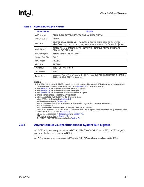
Electrical Specific<strong>at</strong>ionsTable 4.System Bus Signal GroupsGroup NameSignalsAGTL+ InputAGTL+ OutputBPRI#, BR1#, DEFER#, RESET#, RS[2:0]#, RSP#, TRDY#PRDY#AGTL+ I/OA[35:3]#, ADS#, AERR#, AP[1:0]#, BERR#, BINIT#, BNR#, BP[3:2]#, BPM[1:0]#,BR0# 1 , D[63:0]#, DBSY#, DEP[7:0]#, DRDY#, HIT#, HITM#, LOCK#, REQ[4:0]#, RP#CMOS Input 5 A20M#, FLUSH#, IGNNE#, INIT#, LINT0/INTR, LINT1/NMI, PREQ#, PWRGOOD 2 ,SMI#, SLP# 3 , STPCLK#CMOS Output 5 FERR#, IERR#, THERMTRIP# 4System Bus Clock BCLKAPIC Clock PICCLKAPIC I/O 5PICD[1:0]TAP Input 5 TCK, TDI, TMS, TRST#TAP Output 5 TDOPower/O<strong>the</strong>r 6VCC CORE , VCC L2 /VCC 3.3 , VCC 5 , VID[4:0], VTT, VSS, SLOTOCC#, THERMDP, THERMDN,BSEL[1:0], EMI, TESTHI, ReservedNOTES:1. The BR0# pin is <strong>the</strong> only BREQ# signal th<strong>at</strong> is bidirectional. The internal BREQ# signals are mapped on<strong>to</strong>BR# pins after <strong>the</strong> agent ID is determined. See Section 7.0 <strong>for</strong> more in<strong>for</strong>m<strong>at</strong>ion.2. See Section 7.0 <strong>for</strong> in<strong>for</strong>m<strong>at</strong>ion on <strong>the</strong> PWRGOOD signal.3. See Section 7.0 <strong>for</strong> in<strong>for</strong>m<strong>at</strong>ion on <strong>the</strong> SLP# signal.4. See Section 7.0 <strong>for</strong> in<strong>for</strong>m<strong>at</strong>ion on <strong>the</strong> THERMTRIP# signal.5. These signals are specified <strong>for</strong> 2.5 V oper<strong>at</strong>ion.6. VCC CORE is <strong>the</strong> power supply <strong>for</strong> <strong>the</strong> processor core.VCC L2 /VCC 3.3 is described in Section 2.3.VID[4:0] is described in Section 2.6.VTT is used <strong>to</strong> termin<strong>at</strong>e <strong>the</strong> system bus and gener<strong>at</strong>e V REF on <strong>the</strong> processor substr<strong>at</strong>e.VSS is system ground.TESTHI should be connected <strong>to</strong> 2.5 V with a 1 kΩ –10 kΩ resis<strong>to</strong>r.VCC 5 is not connected <strong>to</strong> <strong>the</strong> <strong>Pentium</strong> <strong>III</strong> processor core. This supply is used <strong>for</strong> <strong>the</strong> test equipment and <strong>to</strong>ols.SLOTOCC# is described in Section 7.0.BSEL[1:0] is described in Section 2.8.2 and Section 7.0.EMI pins are described in Section 7.0.THERMDP, THERMDN are described in Section 7.0.2.8.1 Asynchronous vs. Synchronous <strong>for</strong> System Bus SignalsAll AGTL+ signals are synchronous <strong>to</strong> BCLK. All of <strong>the</strong> CMOS, Clock, APIC, and TAP signalscan be applied asynchronously <strong>to</strong> BCLK.All APIC signals are synchronous <strong>to</strong> PICCLK. All TAP signals are synchronous <strong>to</strong> TCK.D<strong>at</strong>asheet 21