Intel Pentium III Processor for the SC242 at 450 MHz to 1.0 GHz
Intel Pentium III Processor for the SC242 at 450 MHz to 1.0 GHz
Intel Pentium III Processor for the SC242 at 450 MHz to 1.0 GHz

Create successful ePaper yourself
Turn your PDF publications into a flip-book with our unique Google optimized e-Paper software.
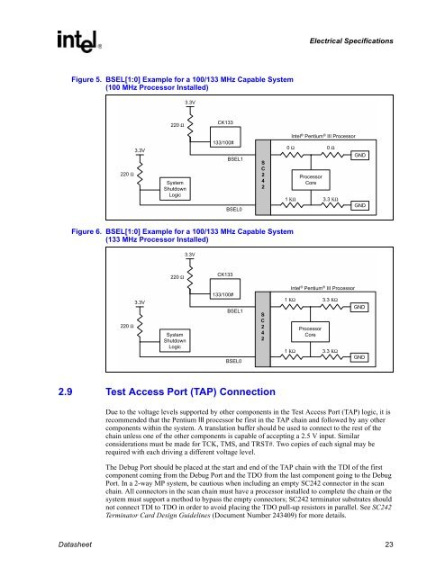
Electrical Specific<strong>at</strong>ionsFigure 5. BSEL[1:0] Example <strong>for</strong> a 100/133 <strong>MHz</strong> Capable System(100 <strong>MHz</strong> <strong>Processor</strong> Installed)3.3V220 ΩCK133220 Ω3.3VSystemShutdownLogic133/100#BSEL1BSEL0<strong>SC242</strong><strong>Intel</strong> ® <strong>Pentium</strong> ® <strong>III</strong> <strong>Processor</strong>0 Ω 0 Ω<strong>Processor</strong>Core1 ΚΩ 3.3 ΚΩGNDGNDFigure 6. BSEL[1:0] Example <strong>for</strong> a 100/133 <strong>MHz</strong> Capable System(133 <strong>MHz</strong> <strong>Processor</strong> Installed)3.3V220 ΩCK133220 Ω3.3VSystemShutdownLogic133/100#BSEL1BSEL0<strong>SC242</strong><strong>Intel</strong> ® <strong>Pentium</strong> ® <strong>III</strong> <strong>Processor</strong>1 ΚΩ 3.3 ΚΩ<strong>Processor</strong>Core1 ΚΩ 3.3 ΚΩGNDGND2.9 Test Access Port (TAP) ConnectionDue <strong>to</strong> <strong>the</strong> voltage levels supported by o<strong>the</strong>r components in <strong>the</strong> Test Access Port (TAP) logic, it isrecommended th<strong>at</strong> <strong>the</strong> <strong>Pentium</strong> <strong>III</strong> processor be first in <strong>the</strong> TAP chain and followed by any o<strong>the</strong>rcomponents within <strong>the</strong> system. A transl<strong>at</strong>ion buffer should be used <strong>to</strong> connect <strong>to</strong> <strong>the</strong> rest of <strong>the</strong>chain unless one of <strong>the</strong> o<strong>the</strong>r components is capable of accepting a 2.5 V input. Similarconsider<strong>at</strong>ions must be made <strong>for</strong> TCK, TMS, and TRST#. Two copies of each signal may berequired with each driving a different voltage level.The Debug Port should be placed <strong>at</strong> <strong>the</strong> start and end of <strong>the</strong> TAP chain with <strong>the</strong> TDI of <strong>the</strong> firstcomponent coming from <strong>the</strong> Debug Port and <strong>the</strong> TDO from <strong>the</strong> last component going <strong>to</strong> <strong>the</strong> DebugPort. In a 2-way MP system, be cautious when including an empty <strong>SC242</strong> connec<strong>to</strong>r in <strong>the</strong> scanchain. All connec<strong>to</strong>rs in <strong>the</strong> scan chain must have a processor installed <strong>to</strong> complete <strong>the</strong> chain or <strong>the</strong>system must support a method <strong>to</strong> bypass <strong>the</strong> empty connec<strong>to</strong>rs; <strong>SC242</strong> termin<strong>at</strong>or substr<strong>at</strong>es shouldnot connect TDI <strong>to</strong> TDO in order <strong>to</strong> avoid placing <strong>the</strong> TDO pull-up resis<strong>to</strong>rs in parallel. See <strong>SC242</strong>Termin<strong>at</strong>or Card Design Guidelines (Document Number 243409) <strong>for</strong> more details.D<strong>at</strong>asheet 23