Intel Pentium III Processor for the SC242 at 450 MHz to 1.0 GHz
Intel Pentium III Processor for the SC242 at 450 MHz to 1.0 GHz
Intel Pentium III Processor for the SC242 at 450 MHz to 1.0 GHz

You also want an ePaper? Increase the reach of your titles
YUMPU automatically turns print PDFs into web optimized ePapers that Google loves.
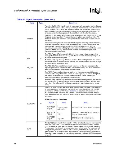
<strong>Intel</strong> ® <strong>Pentium</strong> ® <strong>III</strong> <strong>Processor</strong> Signal DescriptionTable 41. Signal Description (Sheet 6 of 7)Name Type DescriptionRESET#RP#RS[2:0]#RSP#SLOTOCC#II/OIIOAsserting <strong>the</strong> RESET# signal resets all processors <strong>to</strong> known st<strong>at</strong>es and invalid<strong>at</strong>es<strong>the</strong>ir L1 and L2 caches without writing back any of <strong>the</strong>ir contents. For a Power-on or“warm” reset, RESET# must stay active <strong>for</strong> <strong>at</strong> least one millisecond after Vcc COREand CLK have reached <strong>the</strong>ir proper specific<strong>at</strong>ions. On observing active RESET#,all processor system bus agents will deassert <strong>the</strong>ir outputs within two clocks.A number of bus signals are sampled <strong>at</strong> <strong>the</strong> active-<strong>to</strong>-inactive transition of RESET#<strong>for</strong> power-on configur<strong>at</strong>ion. These configur<strong>at</strong>ion options are described in <strong>the</strong> P6Family of <strong>Processor</strong>s Hardware Developer’s Manual (Document Number 244001)<strong>for</strong> details.The processor may have its outputs trist<strong>at</strong>ed via power-on configur<strong>at</strong>ion. O<strong>the</strong>rwise,if INIT# is sampled active during <strong>the</strong> active-<strong>to</strong>-inactive transition of RESET#, <strong>the</strong>processor will execute its Built-in Self-Test (BIST). Whe<strong>the</strong>r or not BIST isexecuted, <strong>the</strong> processor will begin program execution <strong>at</strong> <strong>the</strong> power on Reset vec<strong>to</strong>r(default 0_FFFF_FFF0h). RESET# must connect <strong>the</strong> appropri<strong>at</strong>e pins of allprocessor system bus agents.The RP# (Request Parity) signal is driven by <strong>the</strong> request initi<strong>at</strong>or, and providesparity protection on ADS# and REQ[4:0]#. It must connect <strong>the</strong> appropri<strong>at</strong>e pins ofall processor system bus agents.A correct parity signal is high if an even number of covered signals are low and lowif an odd number of covered signals are low. This definition allows parity <strong>to</strong> be highwhen all covered signals are high.The RS[2:0]# (Response St<strong>at</strong>us) signals are driven by <strong>the</strong> response agent (<strong>the</strong>agent responsible <strong>for</strong> completion of <strong>the</strong> current transaction), and must connect <strong>the</strong>appropri<strong>at</strong>e pins of all processor system bus agents.The RSP# (Response Parity) signal is driven by <strong>the</strong> response agent (<strong>the</strong> agentresponsible <strong>for</strong> completion of <strong>the</strong> current transaction) during assertion of RS[2:0]#,<strong>the</strong> signals <strong>for</strong> which RSP# provides parity protection. It must connect <strong>the</strong>appropri<strong>at</strong>e pins of all processor system bus agents.A correct parity signal is high if an even number of covered signals are low and lowif an odd number of covered signals are low. While RS[2:0]# = 000, RSP# is alsohigh, since this indic<strong>at</strong>es it is not being driven by any agent guaranteeing correctparity.The SLOTOCC# signal is defined <strong>to</strong> allow a system design <strong>to</strong> detect <strong>the</strong> presenceof a termin<strong>at</strong>or card or processor in a <strong>SC242</strong> connec<strong>to</strong>r. Combined with <strong>the</strong> VIDcombin<strong>at</strong>ion of VID[4:0]= 11111 (see Section 2.6), a system can determine if a<strong>SC242</strong> connec<strong>to</strong>r is occupied, and whe<strong>the</strong>r a processor core is present. See <strong>the</strong>table below <strong>for</strong> st<strong>at</strong>es and values <strong>for</strong> determining <strong>the</strong> type of cartridge in <strong>the</strong> <strong>SC242</strong>connec<strong>to</strong>r.<strong>SC242</strong> Occup<strong>at</strong>ion Truth TableSignal Value St<strong>at</strong>usSLOTOCC#VID[4:0]0Anything o<strong>the</strong>rthan ‘11111’<strong>Processor</strong> with core in <strong>SC242</strong> connec<strong>to</strong>r.SLOTOCC#VID[4:0]SLOTOCC#VID[4:0]0111111Any valueTermin<strong>at</strong>or cartridge in <strong>SC242</strong> connec<strong>to</strong>r(i.e., no core present).<strong>SC242</strong> connec<strong>to</strong>r not occupied.SLP#IThe SLP# (Sleep) signal, when asserted in S<strong>to</strong>p-Grant st<strong>at</strong>e, causes processors <strong>to</strong>enter <strong>the</strong> Sleep st<strong>at</strong>e. During Sleep st<strong>at</strong>e, <strong>the</strong> processor s<strong>to</strong>ps providing internalclock signals <strong>to</strong> all units, leaving only <strong>the</strong> Phase-Locked Loop (PLL) still oper<strong>at</strong>ing.<strong>Processor</strong>s in this st<strong>at</strong>e will not recognize snoops or interrupts. The processor willrecognize only assertions of <strong>the</strong> SLP#, STPCLK#, and RESET# signals while inSleep st<strong>at</strong>e. If SLP# is deasserted, <strong>the</strong> processor exits Sleep st<strong>at</strong>e and returns <strong>to</strong>S<strong>to</strong>p-Grant st<strong>at</strong>e, restarting its internal clock signals <strong>to</strong> <strong>the</strong> bus and APIC processorcore units.98 D<strong>at</strong>asheet