warpage and stress concentration nearthe bond wire stitch• Layout of silicon chips on a diepad in a multichip module to minimizedelamination stresses• Thick metal content to reducewafer warpage, which affects handlingin assembly• Metal content balancing in a substrateto reduce warpage, which affectsassembly to PCBsThe role of modeling will grow to influencedesign, materials, and processesused in packaging.DFM at aDvanceD noDesanD its iMpact on DesignFlows: a reality checkManoj Chacko, Product MarketingDirector, Custom IC and Sign Off,Cadence Design SystemsManufacturing improvements via novelmaterials, processes, and new technologiesaren’t keeping up with the marketdemand for ever-shrinking featuredimensions, increasing performance,and low-power requirements. Softwareis now, and will remain, the new keyenabler, as long as there’s a growinggap between design and manufacturing.At 28 nm, the impact of manufacturingvariability on performance, powerconsumption, and yield has become disproportionatelylarger and more complex.Software analysis is critical for effectivelyquantifying and mitigating the impact onboth the physical integrity and parametricperformance of the designs.Physical DFM checks are the finalstep after DRC, especially lithographyprocess check analysis. Litho analysiscan be run on blocks, post routein a design flow, and as the final stepafter DRC. The value of litho checksis clearly evident at the beginning ofa process technology ramp-up. At 28nm, for better predictability of physicaland parametric yield, the lithographycomplexity has moved upstreamto parasitic extraction with changesin the multi orders effects range, andin physical verification in the formof recommended DFM rules or lithoyield detractor patterns in the designrule manuals (Figure 2). At 20 nm,double-patterning technology adds yetanother dimension to the impact ofsilicon printability and connectivity.The increase in design density anduse of third-party IP bring additionalchallenges associated with CMPinducedmetal thickness variation.For example, model-based, ratherthan rule-based, CMP analysis is keyto identifying thickness variations ofthe complete metal stack set. Also, asmore design teams integrate third-partyIP, the metal fill thickness variationsaround the border of the IP are increasing.The IP designer follows the designrules and the density requirements.However, making blocks that are easilyintegrated into different SoC environmentswithout iterations to addressCMP density issues is ineffective.The impact of layout-dependenteffects (LDE) variability on the designis well acknowledged. LDE variabilitycomes primarily from manufacturingchallenges, lithography effects, CMP,and stress, which significantly affectdevice behavior. Varying methods areused to mitigate the LDE issues becauseAALikE This?For more articles like thisone, go to www.edn.com/design/integrated-circuitdesign.of the inability to qualify and quantifyvariability impact at the specifictransistors. LDE cannot be analyzedby considering devices in isolation. Acommon method is to over-margin thetransistors with dummies to minimizethe impact of context problems ondevice performance. Designers needsoftware to help quantify delay andleakage due to LDE, improve theirtraditional methods, and locally optimizethe devices deviating from thespecifications (Figure 3). Timing andpower variability are becoming moresignificant at each new process node,TRADITIONAL STA: A→B 80psDELAY ANALYSIS IGNORING REAL CONTEXT EFFECTSCRITICAL PATH AND TIMING DELAYS WITHOUT CONSIDERING THEIMPACT OF LDE ASSUMES STANDARD NEIGHBORING CONTEXTS.CONTEXT-AWARE STA: A→B ?psDELAY ANALYSIS SHOULD INCLUDE REAL CONTEXT EFFECTSCRITICAL PATH DELAY VARIATION TAKING INTO ACCOUNT LDE IMPACTSHOULD SHOW VARIATION BECAUSE OF REAL CONTEXTS.Figure 2 Lithography complexity has moved upstream to parasitic extraction.BB30 EDN | MAY <strong>2013</strong> [ www.edn.com]
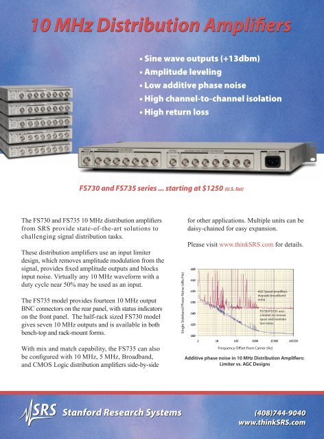
10 MHz Distribution Amplifiers• Sine wave outputs (+13dbm)• Amplitude leveling• Low additive phase noise• High channel-to-channel isolation• High return lossFS730 and FS735 series ... starting at $1250 (U.S. list)The FS730 and FS735 10 MHz distribution ampliersfrom SRS provide state-of-the-art solutions tochallenging signal distribution tasks.These distribution ampliers use an input limiterdesign, which removes amplitude modulation from thesignal, provides xed amplitude outputs and blocksinput noise. Virtually any 10 MHz waveform with aduty cycle near 50% may be used as an input.The FS735 model provides fourteen 10 MHz outputBNC connectors on the rear panel, with status indicatorson the front panel. The half-rack sized FS730 modelgives seven 10 MHz outputs and is available in bothbench-top and rack-mount forms.With mix and match capability, the FS735 can alsobe congured with 10 MHz, 5 MHz, Broadband,and CMOS Logic distribution ampliers side-by-sideSingle Sideband Phase Noise (dBc/Hz)for other applications. Multiple units can bedaisy-chained for easy expansion.Please visit www.thinkSRS.com for details.AGC based amplifiersdegrade broadbandnoise.Frequency Offset from Carrier (Hz)FS730/FS735 usesa limiter to removespurs and maintainlow noise.Additive phase noise in 10 MHz Distribution Amplifiers:Limiter vs. AGC DesignsStanford Research Systems (4<strong>08</strong>)744-9<strong>04</strong>0www.thinkSRS.com


![[270].pdf 37407KB Sep 02 2010 09:55:57 AM - ElectronicsAndBooks](https://img.yumpu.com/50350834/1/185x260/270pdf-37407kb-sep-02-2010-095557-am-electronicsandbooks.jpg?quality=85)
![draaien, A Viruly 1935 OCR c20130324 [320]. - ElectronicsAndBooks](https://img.yumpu.com/49957773/1/190x252/draaien-a-viruly-1935-ocr-c20130324-320-electronicsandbooks.jpg?quality=85)


![20051110 c20051031 [105].pdf 35001KB Feb 18 2009 08:46:32 PM](https://img.yumpu.com/48687202/1/190x253/20051110-c20051031-105pdf-35001kb-feb-18-2009-084632-pm.jpg?quality=85)