201305.pdf 43279KB May 08 2013 11:07:04 PM
201305.pdf 43279KB May 08 2013 11:07:04 PM
201305.pdf 43279KB May 08 2013 11:07:04 PM

You also want an ePaper? Increase the reach of your titles
YUMPU automatically turns print PDFs into web optimized ePapers that Google loves.
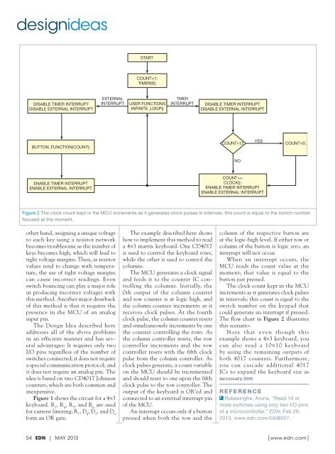
designideasSTARTCOUNT=1;TIMER(0);DISABLE TIMER INTERRUPTDISABLE EXTERNAL INTERRUPTEXTERNALINTERRUPTUSER FUNCTIONSINFINITE_LOOP()TMERINTERRUPTDISABLE TIMER INTERRUPTDISABLE EXTERNAL INTERRUPTBUTTON_FUNCTION(COUNT);COUNT=12YESCOUNT=0;NOENABLE TIMER INTERRUPTENABLE EXTERNAL INTERRUPTCOUNT++CLOCK();ENABLE TIMER INTERRUPTENABLE EXTERNAL INTERRUPTFigure 2 The clock count kept in the MCU increments as it generates clock pulses in intervals; this count is equal to the switch numberfocused at the moment.other hand, assigning a unique voltageto each key using a resistor networkbecomes troublesome as the number ofkeys becomes high, which will lead totight voltage margins. Then, as resistorvalues tend to change with temperature,the use of tight voltage marginscan cause incorrect readings. Evenswitch bouncing can play a major rolein producing incorrect voltages withthis method. Another major drawbackof this method is that it requires thepresence in the MCU of an analoginput pin.The Design Idea described hereaddresses all of the above problemsin an efficient manner and has severaladvantages: It requires only twoI/O pins regardless of the number ofswitches connected; it does not requirea special communication protocol; andit does not require an analog pin. Theidea is based on two CD4017 Johnsoncounters, which are both common andinexpensive.Figure 1 shows the circuit for a 4×3keyboard. R 1, R 4, R 5, and R 6are usedfor current limiting; R 7, D 4, D 5, and D 6form an OR gate.The example described here showshow to implement this method to reada 4×3 matrix keyboard. One CD4017is used to control the keyboard rows,while the other is used to control thecolumns.The MCU generates a clock signaland feeds it to the counter IC controllingthe columns. Initially, the0th output of the column counterand row counter is at logic high, andEDNDI5310 Fig 2.eps DIANEthe column counter increments as itreceives clock pulses. At the fourthclock pulse, the column counter resetsand simultaneously increments by onethe counter controlling the rows. Asthe column controller resets, the rowcontroller increments and the rowcontroller resets with the fifth clockpulse from the column controller. Asclock pulses generate, a count variableon the MCU should be incrementedand should reset to one upon the fifthclock pulse to the row controller. Theoutput of the keyboard is OR’ed andconnected to an external interrupt pinof the MCU.An interrupt occurs only if a buttonpressed when both the row and thecolumn of the respective button areat the logic-high level. If either row orcolumn of the button is logic zero, aninterrupt will not occur.When an interrupt occurs, theMCU reads the count value at themoment; that value is equal to thebutton just pressed.The clock count kept in the MCUincrements as it generates clock pulsesin intervals; this count is equal to theswitch number on the keypad thatcould generate an interrupt if pressed.The flow chart in Figure 2 illustratesthis scenario.Note that even though thisexample shows a 4×3 keyboard, youcan also read a 10×10 keyboardby using the remaining outputs ofboth 4017 counters. Furthermore,you can cascade additional 4017ICs to expand the keyboard size asnecessary.EDNRefeR ence1 Rubasinghe, Aruna, “Read 10 ormore switches using only two I/O pinsof a microcontroller,” EDN, Feb 28,<strong>2013</strong>, www.edn.com/44<strong>08</strong>027.54 EDN | MAY <strong>2013</strong> [ www.edn.com]


![[270].pdf 37407KB Sep 02 2010 09:55:57 AM - ElectronicsAndBooks](https://img.yumpu.com/50350834/1/185x260/270pdf-37407kb-sep-02-2010-095557-am-electronicsandbooks.jpg?quality=85)
![draaien, A Viruly 1935 OCR c20130324 [320]. - ElectronicsAndBooks](https://img.yumpu.com/49957773/1/190x252/draaien-a-viruly-1935-ocr-c20130324-320-electronicsandbooks.jpg?quality=85)


![20051110 c20051031 [105].pdf 35001KB Feb 18 2009 08:46:32 PM](https://img.yumpu.com/48687202/1/190x253/20051110-c20051031-105pdf-35001kb-feb-18-2009-084632-pm.jpg?quality=85)