Systems Reference Library - All about the IBM 1130 Computing ...
Systems Reference Library - All about the IBM 1130 Computing ...
Systems Reference Library - All about the IBM 1130 Computing ...
- No tags were found...

You also want an ePaper? Increase the reach of your titles
YUMPU automatically turns print PDFs into web optimized ePapers that Google loves.
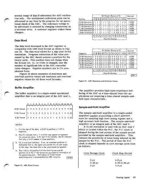
normal range of Mpx/S addresses) for ADC calibrationonly. The multiplexed calibration point can beaddressed at any time by <strong>the</strong> program for an operationalcheck of <strong>the</strong> ADC. The reference voltage tobe addressed is selected by changing connections ona terminal strip. A customer engineer makes <strong>the</strong>sechanges.Data WordThe data word developed in <strong>the</strong> ADC register iscompatible with 1800 word format as shown in Figure33. The data word allows for a sign plus 14-bitresolution. Program conversion of <strong>the</strong> value presentedby <strong>the</strong> ADC should assume a position for <strong>the</strong>binary point. This position does not change when<strong>the</strong> format (14, 11, or 8 bit) is changed; only <strong>the</strong>number of significant bits in <strong>the</strong> ADC convertedvalue changes. Negative numbers are in 2's complementform.Figure 34 shows examples of maximum andoverload positive values and maximum and overloadnegative values for all three word formats.Bit Weight (Powers of 2) DecimalPositive S 13 1211 10 9 817 6 514 3 2 1 0 OL Equivalent14-Bit Maximum 0 1 1 1 1 1 1 1 1 1 1 1 1 1 0 0 +1638214-Bit Overload 0 1 1 1 1 1 1 1 1 1 1 1 1 1 1 1 +1638311-Bit Maximum 0 1 1 1 1 1 1 1 1 1 1 0 1 0 0 0 +1637211-Bit Overload 0 1 1 1 1 1 1 1 1 1 1 1 1 0 0 1 +163808-Bit Maximum 0 1 1 1 1 1 1 1 0 1 0 0 0 0 0 0 +162888-Bit Overload 0 1 1 1 1 1 1 1 1 1 0 0 0 0 0 1 +163520 1 2 3 4 5 6 7 8 9 1011 1213 14 15Word Bit PositionBit Weight (Powers of 2) DecimalNegative S 13 1211 10 9 8 7 6 5 4 3 2 1 0 OL Equivalent14-Bit Maximum 1 0 0 0 0 0 0 0 0 0 0 0 0 0 1 0 -1638314-Bit Overload 1 0 0 0 0 0 0 0 0 0 0 0 0 0 0 1 -1638411-Bit Maximum 1 0 0 0 0 0 0 0 0 0 0 1 1 0 0 0 -1637211-Bit Overload 1 0 0 0 0 0 0 0 0 0 0 0 1 0 0 1 -163808-Bit Maximum 1 0 0 0 0 0 0 0 1 1 0 0 0 0 0 0 -162888-Bit Overload 1 0 0 0 0 0 0 0 0 1 0 0 0 0 0 1 -163520 1 2 3 415 6 7 819110111 1213 14 15Word Bit PositionFigure 34. ADC Maximum and Overload Values117861 1Buffer AmplifierThe buffer amplifier is a single-ended operationalamplifier that is an integral part of <strong>the</strong> ADC mod 1.14-Bit Format11-Bit Format8 Bit FormatNOTES:0 1 2 3 4 5 6 7 8 9 10 11 12 13 14 15IS X X X XXXX X X X X X X XOLS XXXXXXXXXX X 1 0 0 OLSXXXXXXXX 1 0 0 0 0 0 OL1. S is <strong>the</strong> sign of <strong>the</strong> data: a 0-bit is positive; a 1-bit isnegative.2. The X's indicate that a 1- or 0-bit may appear to represent<strong>the</strong> converted value. In 8- and 11-bit formats, <strong>the</strong> 0's indicatethat only a 0 will appear in <strong>the</strong>se positions.3. OL is overload indicator. If on, an overload condition isindicated; that is, <strong>the</strong> signal was outside <strong>the</strong> ±5 volt range.In this case, <strong>the</strong> o<strong>the</strong>r bits in <strong>the</strong> word should be ignored.4. The 1-bit in bit position 9 of <strong>the</strong> 8-bit format and bitposition 1 2 of <strong>the</strong> 11 -bit format are provided for half-adjust of<strong>the</strong> quantizing error. Half-adjust of 14-bit formatquantizing error is accomplished by ADC circuitry.129128A .1Figure 33. ADC Word FormatThe amplifier provides high-input-impedance bufferingof <strong>the</strong> ADC on a time-shared basis for applicationsnot requiring a time-shared sample-andholdinput characteristic.Sample-and-Hold AmplifierThe sample-and-hold amplifier is a single-endedamplifier capable of providing a short aperturetime for sampling high level analog signals and ahigh accuracy hold function. The sample-and-holdamplifier is an integral part of <strong>the</strong> ADC mod 2.If 14-bit resolution is used with an ADC mod 2which is located within <strong>the</strong> P-C , <strong>the</strong> P-C clock isstopped during <strong>the</strong> last portion of <strong>the</strong> sample periodprovided by <strong>the</strong> sample-and-hold amplifier. Thisreduces <strong>the</strong> possibility of noise being induced on <strong>the</strong>sample by <strong>the</strong> P-C. The period of time <strong>the</strong> P-Cclock is stopped depends on core storage cycle timeas follows:Core Storage Cycle Clock Stop Period2 As2.25 ps4 gs1-3 gs0.75-3.00 As1-5 /IsAnalog Input 97