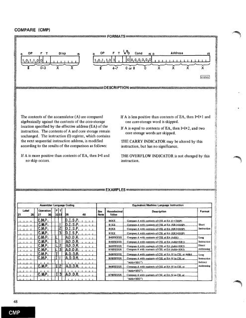
COMPARE (CMP)FORMATS0 OP F T Disp 150 OP1 110111110 01 1 11111 111B 0-3 X XDESCRIPTIONThe contents of <strong>the</strong> accumulator (A) are comparedalgebraically against <strong>the</strong> contents of <strong>the</strong> core-storagelocation specified by <strong>the</strong> effective address (EA) of <strong>the</strong>instruction. The contents of A and core storage remainunchanged. The instruction (I) register, which contains<strong>the</strong> next sequential instruction address, is modifiedaccording to <strong>the</strong> results of <strong>the</strong> comparison as follows:If A is more positive than contents of EA, <strong>the</strong>n 1=I andno skip occurs.If A is less positive than contents of EA, <strong>the</strong>n 1=1+1 andone core-storage word is skipped.If A is equal to contents of EA, <strong>the</strong>n 1=1+2, and twocore storage words are skipped.THE CARRY INDICATOR may be altered by thisinstruction, but has no significance.THE OVERFLOW INDICATOR is not changed by thisinstruction.EXAMPLESAssembler Language CodingEquivalent Machine Language InstructionLabel21 25Operation27 30F T323335 40SeeNoteHexadecimalValueDescriptionFormat1 1 , C,M,P, D,I,SIP, 1 BOXX Compare A with contents of CSL at EA (I + DISP)1 t 1 CIMIP 1 I D1I1S,P1,B 1XX Corn are A with contents of CSL at EA . 1 +ii •i i 1 CIMIP, 2 D,I,,P, S, 1B2XX Compare A with contents of CSL at EA (XR2+DISP)1 1 1 CAR I 3 D,I,S,P, , 1 B3XX Compare A with contents of CSL at EA (XR3+DISP)1 I 1 CM,P, L A,D,D,R, , I B400XXXX Compare A with contents of CSL at EA (Addr) LongShortInstruction1 1 1 CIM,P1 L I A,D,D,R, , 1 B500XXXX Compare A with contents of CSL at EA (Addr+XR1)Instructioni 1 / C IMIP / L 2 A,D,D,R, 1 1 B600XXXX Compare A with contents of CSL at EA (Addr+XR2)DirectC,M,P,Addressing3 A,D,D,R, 1 1 B70030001 Compare A with contents of CSL at EA (Addr+XR3)1 1 1 CIM,P1 L A,D.D,R,1B480XXXX Compare A with contents of CSL at EA (V in CSL at Adds) LongI 1 I C,M1P, I I A,D,D,R,,13580XXXX _ Compare A with contents of CSL at EA (V in CSL at Instructioni j I 1 1 1I I I I1 1"Addr+)(12 1")Indirect1 , 1 C,M,P, I 2 A,D,D,R, I 1 B680XXXX Compare A with contents of CSL at EA (V in CSL atAddressingi I 1 1 1 1 1 1 1 1 1 1 1 1 "Addr+XR2")1 / 1 CIMIP 1 I 3 A,D,D,R, I I B780XXXX Compare A with contents of CSL at EA (yin CSL at1 1 1 1 1 1 1 1 1 i 1 1 1 1 "Addr+XR3'')SitalleeetatieMEIX=22 X__ _48CMP
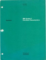
DOUBLE COMPARE (DCM)oFORMATS0 OP F TDisp 150 OPF T I A B O Cond Address IS15 01 1 011 1 1 1 11 01 1 11 1 1 i! IIIB 8-B X X1 1 1 0 1 1 1 1 1 III I I 1010 1 0 1 0 1 0 1 0 /01 1 1 1 1 1 1 IB C-F 0 or 8 0 X X X X117174 BIDESCRIPTIONThe contents of <strong>the</strong> accumulator (A) and its extension(Q) form a 32-bit double-precision word which is comparedalgebraically against <strong>the</strong> contents of <strong>the</strong> corestorage location specified by <strong>the</strong> effective address (EA)of <strong>the</strong> instruction and <strong>the</strong> next higher core-storage location(EA + 1). The contents of A, Q, EA, and EA + 1remain unchanged. The instruction (I) register, whichcontains <strong>the</strong> next sequential instruction address, ismodified according to <strong>the</strong> results of <strong>the</strong> comparison asfollows:If A and Q is more positive than <strong>the</strong> contents of EAand EA + 1, <strong>the</strong>n 1=1 and no skip occurs.If A and Q is less positive than <strong>the</strong> contents of EA andEA + 1, <strong>the</strong>n 1=1+1 and one core-storage word isskipped.If A and Q is equal to <strong>the</strong> contents of EA and EA + 1,<strong>the</strong>n 1=1+2 and two core storage words are skipped.The EA must be even for correct operation. If <strong>the</strong>EA is odd, A and Q are both compared against <strong>the</strong> contentsof EA.THE CARRY INDICATOR may be altered by this instruction,but has no significance.THE OVERFLOW INDICATOR is not changed bythis instruction.amom000mooang000moo EXAMPLESAssembler Language CodingEquivalent Machine Language Instruction21Label25Operation27 30FT323335 40SeeNoteHexadecimalValueDescriptionFormatI I I D,C,M, DII,S1P1 I I I I B8XX • Compare A and Q with contents of CSL at EA (I + DISP)i i i , and EA + 1i 1 I D,C,M, I D,I ,S,P, i I B9XX Compare A and .0 with contents of CSL at EA (XR1+DISP)i I I I 1 I 1 2 I I I I I I and EA + 1i t DIC,M, 2 D, I ,S,P, , I BAXX Compare A and Q with contents of CSL at EA (XR2+DISP)I I i 1 1 1 i and EA + I1 I D,C,M, 3 D,I ,S ,P, I I I BBXX Compare A and Q with contents of CSL at EA (XR3+DISP)I I I I I ,,,, i and EA + 1, , D,C,M, L A,D,D,R, , I BCOOXXX Compare A and Q with contents of CSL at EA (Addr) andI I I I i i I i EA + 1, , I D I C,M, L I A I D ,D,R, I i I BDOOXXXX Compare A and Q with contents of CSL at EA (Addr+XR1)I I I , , , i I I I i and EA + 1, , I D,C,M, L 2 A,D,D,R, 1 I , BEOOXXXX Compare A and Q with contents of CSL at EA (Addr+XR2)I I 1 t I I i 1 1 1 1 1 I I and EA + 1I I I D I C,M, L 3 A I D I D,R, I I I I BF003000( Compare A and Q with contents of CSL at EA (Addr+XR3)i I , 1 1 i 1 1 i and EA + 1I I I D,C,M1 I A,D,D RI I I I I BC8OXXXX Compare A and Q with contents of CSL at EA (V in CSL atI I I I 11 I I I I I I I I Addr) and EA + 1, IBDROXX X Compare A and 0 with contents of CSL at EA (V in CSL atI I I I I / I I II"Addr+XR1") and EA + 1I , , 1 D,C,M, I I A,D,D,R, 1 I, , I D,C,M, I 2 A I D ,D,R, I I BE8030CXX Compare A and 0 with contents of CSL at EA (V in CSL atI I I I i III I "Addr+XR2") and F + 11 I I 0,C ,M, I 3 OD 1R1 i BFROXXXX Compare A and 0 with contents of CST at EA (V in ('SL atI i I I I I, 1 i "Addr+XR3") and EA + 1REEMEREMBESIMESEROLShortInstructionLongInstructionDirectAddressingLongInstructionIndirectAddressingInstruction Set 49DCM
- Page 1 and 2:
File No. 1800-01Order No. GA26-5918
- Page 3 and 4:
ContentsINTRODUCTION 1SYSTEM DESCRI
- Page 5 and 6: Thermocouple Conversion ExampleConv
- Page 7: Status Character 2412790 ADAPTER PR
- Page 12: Processor - ControllerCoreStorageOu
- Page 16 and 17: Page of GA26-5918-8Revised July 14,
- Page 18 and 19: egister or the index register speci
- Page 20 and 21: Short InstructionDDOne WordInstruct
- Page 22 and 23: Instruction SetThe 1800 system inst
- Page 24 and 25: LOAD ACCUMULATOR (LD)FORMATS oitamw
- Page 26 and 27: STORE ACCUMULATOR (STO)FORMATSF 0 O
- Page 28 and 29: LOAD INDEX (LDX)0 OP F T Disp 151 0
- Page 30 and 31: STORE STATUS (STS) Store Status Fun
- Page 32 and 33: LOAD STATUS (LDS)117165 A1DESCRIPTI
- Page 34 and 35: Page of GA26-5918-8Revised July 14,
- Page 36 and 37: SUBTRACT DOUBLE (SD).fartzaielTmEas
- Page 38: DIVIDE (D)FORMATS0 OP F T DispF T I
- Page 41 and 42: LOGICAL EXCLUSIVE OR (EOR)'FORMATS
- Page 43 and 44: SHIFT LEFT A AND Q (SLT)altkae..,.:
- Page 46 and 47: SHIFT RIGHT LOGICAL A (SRA)FORMAT s
- Page 48 and 49: ROTATE RIGHT A AND Q (RTE)FORMAT ta
- Page 50 and 51: BRANCH OR SKIP ON CONDITION (BSC OR
- Page 52 and 53: a4.-4KA4rE4.7.9.4.&.4VA/M4:14/24...
- Page 54 and 55: ',V.71..1.41VV4-02,P2A,V4,1%1,L—N
- Page 58 and 59: Page of GA26-5918-8Revised July 14,
- Page 60 and 61: MachineCyclesAUGEND (A-reg) and ADD
- Page 62 and 63: Page of GA26-5918-8Revised July 14,
- Page 64 and 65: Page of GA26-5918-8Revised July 14,
- Page 66 and 67: chain is accomplished as follows: T
- Page 68 and 69: Page of GA26-5918-8Revised July 14,
- Page 70 and 71: Page of GA26-5918-8Revised July 14,
- Page 72 and 73: Page of GA26-5918-8Revised July 14,
- Page 74 and 75: InterruptTo allow for coordination
- Page 76 and 77: Page of GA26-5918-8Revised July 14,
- Page 78 and 79: Page of GA26-5918-8Revised July 14,
- Page 80 and 81: After a request for service has bee
- Page 82 and 83: 2. The forced BSI with indirect add
- Page 84 and 85: Storage ProtectionStorage protectio
- Page 86 and 87: Page of GA26-5918-8Revised January
- Page 88 and 89: Processor-Controller ConsoleThe pro
- Page 90 and 91: 117674,Figure 23. Console Pushbutto
- Page 92 and 93: Page of GA26-5918-8Revised July 14,
- Page 94 and 95: Page of GA26-5918-8Revised July 14,
- Page 96 and 97: DATA FLOW DISPLAYSSix rows of light
- Page 98 and 99: This command causes the console int
- Page 100 and 101: High -LevelHigh -Level Low-LevelLow
- Page 102 and 103: Page of GA26-5918-8Revised July 14,
- Page 104 and 105: CUSTOM ELEMENT: This element is ava
- Page 106 and 107:
The clock stop period does not dire
- Page 108 and 109:
Numberingwithin 18511851's withMult
- Page 110 and 111:
selected analog signal to a digital
- Page 112 and 113:
Page of GA26-5918-8Revised July 14,
- Page 114 and 115:
0 1 2 3 4 5 8 7 0 9 10 14 15Indicat
- Page 116 and 117:
Direct Program Control Operations P
- Page 118 and 119:
Temp TempF C1652° 9001472° 81292
- Page 120 and 121:
2. Determine the ADC reading (Q val
- Page 122 and 123:
Digital InputDigital input features
- Page 124 and 125:
ead operation without external sync
- Page 126 and 127:
AdapterFirstSecondThirdFourthFifthS
- Page 128 and 129:
the next input group address (conta
- Page 130 and 131:
status word (PISW), the PISW is rea
- Page 132 and 133:
ProcessorControllerOut Bus(16 - Bit
- Page 134 and 135:
DAC reference voltage used in devel
- Page 136 and 137:
126 is assigned to the second group
- Page 138 and 139:
The input/output control command (I
- Page 140 and 141:
Page of GA26-5918-8Revised July 14,
- Page 142 and 143:
1053/1816 Printer IOCC'sCE ModeSpec
- Page 144 and 145:
Keyboard entries are not printed au
- Page 146 and 147:
error is detected, the program may
- Page 148 and 149:
the keyboard into a storage-protect
- Page 150 and 151:
Channel••• ••••• 14
- Page 152 and 153:
READER ANY ERROR: This indicator tu
- Page 154 and 155:
Page of GA26-5918-8Revised July 14,
- Page 156 and 157:
Even-Numbered ColumnsOdd-Numbered C
- Page 158 and 159:
1442 DSW Interrupt IndicatorsFigure
- Page 160 and 161:
The preceding examples show that if
- Page 162 and 163:
CharHexCore Storage BitsTypebar2 5
- Page 164 and 165:
Page of GA26-5918-8Revised July 14,
- Page 166 and 167:
CE PRINTER BUSY: When the 1443 is i
- Page 168 and 169:
DrumDownDRUM FAST RUN: This switch
- Page 170 and 171:
1627 DSW Noninterrupt IndicatorsFig
- Page 172 and 173:
120255A1Each track is divided into
- Page 174 and 175:
This command places the disk storag
- Page 176 and 177:
ANY ERROR: This indicator turns on
- Page 178 and 179:
LogicalDataRecordIBGapLRCIBGap.._01
- Page 180 and 181:
A tape mark read from seven-track t
- Page 182 and 183:
Modifier bits perform the five func
- Page 184 and 185:
an XIO initialize read operation wi
- Page 186 and 187:
Communications AdapterINTRODUCTIONT
- Page 188 and 189:
character (bit positions 0 through
- Page 190 and 191:
Bit PositionsP, 7, 6, 54, 3, 2, 100
- Page 192 and 193:
Standard replies as well as NAK cau
- Page 194 and 195:
either seeking characters received
- Page 196 and 197:
CA IOCC'sInitialize Write0 15 0 4 8
- Page 198 and 199:
TIMEOUT: This indicator turns on, c
- Page 200 and 201:
0 I 2 3 4 5 6 7 8 9 10 11 i2 13 14
- Page 202 and 203:
ETB, ETX, AND ENQ: These characters
- Page 204 and 205:
.■••.0■-3toCOc.nroz0F21.0fa
- Page 206 and 207:
Selector ChannelThe selector channe
- Page 208 and 209:
CCW Word 1 CCW Word 2 CCW Word 315B
- Page 210 and 211:
Page of GA26-5918-8Revised July 14,
- Page 212 and 213:
limited to the number of sense byte
- Page 214 and 215:
CSW Word 1 CSW Word 2 CSW Word 3 CS
- Page 216 and 217:
CSW Word 2 CSW Word 3CSW Word 40 3
- Page 218 and 219:
Termination of an operation with a
- Page 220 and 221:
Device end, when subsequently provi
- Page 222 and 223:
System /360 AdapterINTRODUCTIONThe
- Page 224 and 225:
specified by the channel command wo
- Page 226 and 227:
ATTENTION: This status indicates th
- Page 228 and 229:
Page of GA26-5918-8Revised July 14,
- Page 230 and 231:
HALT: This bit turns on, causing an
- Page 232 and 233:
Page of GA26-5918-8Revised July 14,
- Page 234 and 235:
Start Byte AS Address Byte Device A
- Page 236 and 237:
Page of GA26-5918-8Revised July 14,
- Page 238 and 239:
Read data request causes the adapte
- Page 240 and 241:
If a 1053 Printer is addressed by t
- Page 242 and 243:
specific 16-word block within the c
- Page 244 and 245:
LCCBWord1Address Word(Active Frame)
- Page 246 and 247:
channel active is interrogated. If
- Page 248 and 249:
Form GA26-5918-8Page Revised 10/1/7
- Page 250 and 251:
AREA STATION LOCAL I/O TRANSACTION
- Page 252 and 253:
Form GA26-5918-8Page Revised 10/1/7
- Page 254 and 255:
244Form GA26-5918-8Page Added 10/1/
- Page 256 and 257:
Page of GA26-5918-8Revised July 14,
- Page 258 and 259:
Form GA26-5918-8Page Revised 10/1/7
- Page 260 and 261:
Form GA26-5918-8Page Revised 10/1/7
- Page 262 and 263:
When all segments are bypassed modi
- Page 264 and 265:
0. It can occur only during a read
- Page 266 and 267:
Page of GA26-5918-8Revised July 14,
- Page 268 and 269:
HexadecimalValueDouble Compare (DCM
- Page 270 and 271:
Appendix B. I/O Device AddressingTh
- Page 272 and 273:
1054 AND 1055 PAPER TAPEWRITE: Punc
- Page 274 and 275:
INITIALIZE WRITE: Move contents of
- Page 276 and 277:
INITIALIZE READ: Move tape data to
- Page 278 and 279:
AREA FEATURE 0 1 2 3 4 5 6 7 8 9•
- Page 280 and 281:
Form GA26-5918-8Page Revised 10/1/7
- Page 282 and 283:
Page of GA26-5918-8Revised July 14,
- Page 284 and 285:
Clear (Continued)Storage (Continued
- Page 286 and 287:
Converting Thermocouple Characteris
- Page 288 and 289:
Page of GA26-5918-8Revised July 14,
- Page 290 and 291:
4Input/Output Control (Continued)On
- Page 292 and 293:
Loop Channel (Continued)Control Blo
- Page 294 and 295:
Pulse OutputDescription of 125Timer
- Page 296 and 297:
Storage ProtectBit (S) 10Bit Light
- Page 298 and 299:
1053 Printer (Continued)Maximum Rat
- Page 300 and 301:
1810 Disk Storage (Continued)Read/W
- Page 302:
Form GA26-5918-8Page Revised 10/1/7
- Page 305:
IBM Technical Newsletter File Numbe
- Page 308 and 309:
^;``
- Page 311 and 312:
• READER'S COMMENT FORM•▪ IBM
- Page 313 and 314:
• READER'S COMMENT FORM• IBM 18
- Page 315 and 316:
• READER'S COMMENT FORM• IBM 18