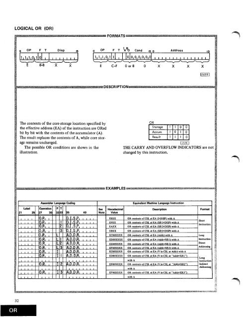
LOGICAL OR (OR)FORMATS mmigiaOP F T Disp 151 1 1 / 1 1 1 0 1 1 1 0 1 1 I 1 1 1 1 1 1 1E 8-B -X XI0 OP F T AB 0 Cond 15 0 Address1511 1 1 1 1 / 0,1111 I 101010,01010101E C-F 0 or 8 0 X X X X1/7177B 1D ESCR I PTION 5101ESEET777:77=._.The contents of <strong>the</strong> core-storage location specified by<strong>the</strong> effective address (EA) of <strong>the</strong> instruction are ORedbit by bit with <strong>the</strong> contents of <strong>the</strong> accumulator (A).The result replaces <strong>the</strong> contents of A, while core storageremains unchanged.The possible OR conditions are shown in <strong>the</strong>illustration.ORStorage 1 1 0 0Accum 1 0 1 0Result 1 1 1 0117178THE CARRY AND OVERFLOW INDICATORS are notchanged by this instruction.A EXAMPLESAssembler Language CodingEquivalent Machine Language Instruction21Label25Operation27 30FT323335 40SeeNoteHexadecimalValueDescriptionFormat1 1 I 0,R 1 I D1I,S,P, 1 I EBXX OR contents of CSL at EA (I+DISP) with Ai1 0,13, I I D,I,S,P, 1 E9XX OR contents of CSL at EA (XRI+DISP) with A1 1 I 0,R, 2 D,I ,S 1P 1 1EAXX OR contents of CSL at EA (XR2+DISP) with AI I I 0 1 R, I 3 D,I,S,P, , 1 EBXX OR contents of CSL at EA (XR3+DISP) with AI I I 01R1 I L A,D,D1R, , ECOOXXXX OR contents of CSL at EA (Addy) with A Long1 I I 0 1 R, I L I A,D,D,R, I I , 1 EDOOXXXX OR contents of CSL at EA (Addr+XR1) with Ai 1 I 0,R, L 2 A,D,D,R, I I I EE00XXXX OR contents of CSL at EA (Addr+XR2) with AI I I 0,R, I L 3 A,D,D,R, I I EFOOXXXX OR contents of CSL at EA (Addr+XR3) with A1 1 1 0,13, 1 I A,D,D,R, 1 1 I EC80XXXX OR contents of CSL at EA (V in CSL at Addr) with AI I I 0,R, I I A,D,D,R, I I ED80XXXX OR contents of CSL at EA (V in CSL at "Addr+XRI")I I I 1 I I I I I I with A, , 1 0,R, I 2 AID,D,R, I1 I I EE80XXXX OR contents of CSL at EA (V in CSL at "Addr+XR2")I I i I III!Iwith AI I I 0,R, 13 A,D,D,R, I I , EF80)0CXX OR contents of CSL at EA (V in CSL at "Addr+XR3")1 1 1 i i I I I I I 1 1 I I with AShortInstructionInstructionDirectAddressingLongInstructionIndirectAddressingOMB' _ 1tw _BM= _32OR
LOGICAL EXCLUSIVE OR (EOR)'FORMATS 0OP F T Disp 15F T 4 8 O Cond 150 Address11111111010 11111111111 0 ,1 003111 ► I lolo,o 1 o,o,o 1 o1 , ► ►► ► ►IF 0-3 X XDESCRIPTIONThe contents of <strong>the</strong> core-storage location specified by<strong>the</strong> effective address (EA) of <strong>the</strong> instruction are exclusiveORed bit by bit with <strong>the</strong> contents of <strong>the</strong> accumulator(A). The result replaces <strong>the</strong> contents of A, whilecore storage remains unchanged.The possible exclusive ,OR conditions are shown in<strong>the</strong> illustration.Storage 1 1 0 0Accum 1 0 1 0Result 0 1 11 718 0THE CARRY AND OVERFLOW INDICATORS are notchanged by this instruction.EXAMPLES =Assembler Language CodingEquivalent Machine Language InstructionLabel21 25Operation27 30FT323335 40SeeNoteHexadecimalValueDescriptionFormat, , 1 E 1 0 1R, DIIISIP, 1 FOXX EOR contents of CSL at EA (I+DISP) with A1 , , E l O,R, I D,I,S,P, 1 1 1 I FIXX EOR contents of CSL at EA (XRI+DISP) with A1 1 1 E,O 1 R, 2 D,I 1 S,P, t I F2XX EOR contents of CSL at EA (XR2+DISP) with A1 1 I E,01 R, 3 D,I,S,P, t F3XX EOR contents of CSL at EA (XR3+DISP) with AShortInstruction1 1 1 E 101R, L A,D,D,R, , 1 F400XXXX EOR contents of CSL at EA (Addr) with A LongInstruction1 1 l E10,R, L I A,D,D,R, , I F500XXXX EOR contents of CSL at EA (Addr+XRI)with ADirect1 1 i E LOP, L 2 AID,D,R, I 1 F600XXXX EOR contents of CSL at EA (Addr+XR2) with AAddressing1 , , E10,R, L 3 A,D1D,R, 1 I 1 1 F7003000( EOR contents of CSL at EA (Addr+XR3) with A1 I 1 Ei(),R, I A,D,D,R, , F4807000C EOR contents of CSL at EA (V in CSL at Addr) with A, , , E,O,R, I I A,D,D,R, I I F580XXXX EOR contents of CSL at EA (V in CSL at "Addr+XR I") LongInstructionI I I I I I I I I 1 I I I with AtIndirect1 1 I E,O,R, I 2 A,D,D,R, , 1 F680XXXX EOR contents of CSL at EA (V in CSL at "Addr+XR2")Addressing1 1 1 I I 1 I I I I with A, , , E 10 1R, 13 A,D,D,R, 1 1 F780XXXX EOR contents of CSL at EA (V in CSL at "Addr+XR3")1, 1 I I I I 1 1 1 1 1 1 1 with AInstruction Set 33EOR
- Page 1 and 2: File No. 1800-01Order No. GA26-5918
- Page 3 and 4: ContentsINTRODUCTION 1SYSTEM DESCRI
- Page 5 and 6: Thermocouple Conversion ExampleConv
- Page 7: Status Character 2412790 ADAPTER PR
- Page 12: Processor - ControllerCoreStorageOu
- Page 16 and 17: Page of GA26-5918-8Revised July 14,
- Page 18 and 19: egister or the index register speci
- Page 20 and 21: Short InstructionDDOne WordInstruct
- Page 22 and 23: Instruction SetThe 1800 system inst
- Page 24 and 25: LOAD ACCUMULATOR (LD)FORMATS oitamw
- Page 26 and 27: STORE ACCUMULATOR (STO)FORMATSF 0 O
- Page 28 and 29: LOAD INDEX (LDX)0 OP F T Disp 151 0
- Page 30 and 31: STORE STATUS (STS) Store Status Fun
- Page 32 and 33: LOAD STATUS (LDS)117165 A1DESCRIPTI
- Page 34 and 35: Page of GA26-5918-8Revised July 14,
- Page 36 and 37: SUBTRACT DOUBLE (SD).fartzaielTmEas
- Page 38: DIVIDE (D)FORMATS0 OP F T DispF T I
- Page 43 and 44: SHIFT LEFT A AND Q (SLT)altkae..,.:
- Page 46 and 47: SHIFT RIGHT LOGICAL A (SRA)FORMAT s
- Page 48 and 49: ROTATE RIGHT A AND Q (RTE)FORMAT ta
- Page 50 and 51: BRANCH OR SKIP ON CONDITION (BSC OR
- Page 52 and 53: a4.-4KA4rE4.7.9.4.&.4VA/M4:14/24...
- Page 54 and 55: ',V.71..1.41VV4-02,P2A,V4,1%1,L—N
- Page 56 and 57: COMPARE (CMP)FORMATS0 OP F T Disp 1
- Page 58 and 59: Page of GA26-5918-8Revised July 14,
- Page 60 and 61: MachineCyclesAUGEND (A-reg) and ADD
- Page 62 and 63: Page of GA26-5918-8Revised July 14,
- Page 64 and 65: Page of GA26-5918-8Revised July 14,
- Page 66 and 67: chain is accomplished as follows: T
- Page 68 and 69: Page of GA26-5918-8Revised July 14,
- Page 70 and 71: Page of GA26-5918-8Revised July 14,
- Page 72 and 73: Page of GA26-5918-8Revised July 14,
- Page 74 and 75: InterruptTo allow for coordination
- Page 76 and 77: Page of GA26-5918-8Revised July 14,
- Page 78 and 79: Page of GA26-5918-8Revised July 14,
- Page 80 and 81: After a request for service has bee
- Page 82 and 83: 2. The forced BSI with indirect add
- Page 84 and 85: Storage ProtectionStorage protectio
- Page 86 and 87: Page of GA26-5918-8Revised January
- Page 88 and 89: Processor-Controller ConsoleThe pro
- Page 90 and 91:
117674,Figure 23. Console Pushbutto
- Page 92 and 93:
Page of GA26-5918-8Revised July 14,
- Page 94 and 95:
Page of GA26-5918-8Revised July 14,
- Page 96 and 97:
DATA FLOW DISPLAYSSix rows of light
- Page 98 and 99:
This command causes the console int
- Page 100 and 101:
High -LevelHigh -Level Low-LevelLow
- Page 102 and 103:
Page of GA26-5918-8Revised July 14,
- Page 104 and 105:
CUSTOM ELEMENT: This element is ava
- Page 106 and 107:
The clock stop period does not dire
- Page 108 and 109:
Numberingwithin 18511851's withMult
- Page 110 and 111:
selected analog signal to a digital
- Page 112 and 113:
Page of GA26-5918-8Revised July 14,
- Page 114 and 115:
0 1 2 3 4 5 8 7 0 9 10 14 15Indicat
- Page 116 and 117:
Direct Program Control Operations P
- Page 118 and 119:
Temp TempF C1652° 9001472° 81292
- Page 120 and 121:
2. Determine the ADC reading (Q val
- Page 122 and 123:
Digital InputDigital input features
- Page 124 and 125:
ead operation without external sync
- Page 126 and 127:
AdapterFirstSecondThirdFourthFifthS
- Page 128 and 129:
the next input group address (conta
- Page 130 and 131:
status word (PISW), the PISW is rea
- Page 132 and 133:
ProcessorControllerOut Bus(16 - Bit
- Page 134 and 135:
DAC reference voltage used in devel
- Page 136 and 137:
126 is assigned to the second group
- Page 138 and 139:
The input/output control command (I
- Page 140 and 141:
Page of GA26-5918-8Revised July 14,
- Page 142 and 143:
1053/1816 Printer IOCC'sCE ModeSpec
- Page 144 and 145:
Keyboard entries are not printed au
- Page 146 and 147:
error is detected, the program may
- Page 148 and 149:
the keyboard into a storage-protect
- Page 150 and 151:
Channel••• ••••• 14
- Page 152 and 153:
READER ANY ERROR: This indicator tu
- Page 154 and 155:
Page of GA26-5918-8Revised July 14,
- Page 156 and 157:
Even-Numbered ColumnsOdd-Numbered C
- Page 158 and 159:
1442 DSW Interrupt IndicatorsFigure
- Page 160 and 161:
The preceding examples show that if
- Page 162 and 163:
CharHexCore Storage BitsTypebar2 5
- Page 164 and 165:
Page of GA26-5918-8Revised July 14,
- Page 166 and 167:
CE PRINTER BUSY: When the 1443 is i
- Page 168 and 169:
DrumDownDRUM FAST RUN: This switch
- Page 170 and 171:
1627 DSW Noninterrupt IndicatorsFig
- Page 172 and 173:
120255A1Each track is divided into
- Page 174 and 175:
This command places the disk storag
- Page 176 and 177:
ANY ERROR: This indicator turns on
- Page 178 and 179:
LogicalDataRecordIBGapLRCIBGap.._01
- Page 180 and 181:
A tape mark read from seven-track t
- Page 182 and 183:
Modifier bits perform the five func
- Page 184 and 185:
an XIO initialize read operation wi
- Page 186 and 187:
Communications AdapterINTRODUCTIONT
- Page 188 and 189:
character (bit positions 0 through
- Page 190 and 191:
Bit PositionsP, 7, 6, 54, 3, 2, 100
- Page 192 and 193:
Standard replies as well as NAK cau
- Page 194 and 195:
either seeking characters received
- Page 196 and 197:
CA IOCC'sInitialize Write0 15 0 4 8
- Page 198 and 199:
TIMEOUT: This indicator turns on, c
- Page 200 and 201:
0 I 2 3 4 5 6 7 8 9 10 11 i2 13 14
- Page 202 and 203:
ETB, ETX, AND ENQ: These characters
- Page 204 and 205:
.■••.0■-3toCOc.nroz0F21.0fa
- Page 206 and 207:
Selector ChannelThe selector channe
- Page 208 and 209:
CCW Word 1 CCW Word 2 CCW Word 315B
- Page 210 and 211:
Page of GA26-5918-8Revised July 14,
- Page 212 and 213:
limited to the number of sense byte
- Page 214 and 215:
CSW Word 1 CSW Word 2 CSW Word 3 CS
- Page 216 and 217:
CSW Word 2 CSW Word 3CSW Word 40 3
- Page 218 and 219:
Termination of an operation with a
- Page 220 and 221:
Device end, when subsequently provi
- Page 222 and 223:
System /360 AdapterINTRODUCTIONThe
- Page 224 and 225:
specified by the channel command wo
- Page 226 and 227:
ATTENTION: This status indicates th
- Page 228 and 229:
Page of GA26-5918-8Revised July 14,
- Page 230 and 231:
HALT: This bit turns on, causing an
- Page 232 and 233:
Page of GA26-5918-8Revised July 14,
- Page 234 and 235:
Start Byte AS Address Byte Device A
- Page 236 and 237:
Page of GA26-5918-8Revised July 14,
- Page 238 and 239:
Read data request causes the adapte
- Page 240 and 241:
If a 1053 Printer is addressed by t
- Page 242 and 243:
specific 16-word block within the c
- Page 244 and 245:
LCCBWord1Address Word(Active Frame)
- Page 246 and 247:
channel active is interrogated. If
- Page 248 and 249:
Form GA26-5918-8Page Revised 10/1/7
- Page 250 and 251:
AREA STATION LOCAL I/O TRANSACTION
- Page 252 and 253:
Form GA26-5918-8Page Revised 10/1/7
- Page 254 and 255:
244Form GA26-5918-8Page Added 10/1/
- Page 256 and 257:
Page of GA26-5918-8Revised July 14,
- Page 258 and 259:
Form GA26-5918-8Page Revised 10/1/7
- Page 260 and 261:
Form GA26-5918-8Page Revised 10/1/7
- Page 262 and 263:
When all segments are bypassed modi
- Page 264 and 265:
0. It can occur only during a read
- Page 266 and 267:
Page of GA26-5918-8Revised July 14,
- Page 268 and 269:
HexadecimalValueDouble Compare (DCM
- Page 270 and 271:
Appendix B. I/O Device AddressingTh
- Page 272 and 273:
1054 AND 1055 PAPER TAPEWRITE: Punc
- Page 274 and 275:
INITIALIZE WRITE: Move contents of
- Page 276 and 277:
INITIALIZE READ: Move tape data to
- Page 278 and 279:
AREA FEATURE 0 1 2 3 4 5 6 7 8 9•
- Page 280 and 281:
Form GA26-5918-8Page Revised 10/1/7
- Page 282 and 283:
Page of GA26-5918-8Revised July 14,
- Page 284 and 285:
Clear (Continued)Storage (Continued
- Page 286 and 287:
Converting Thermocouple Characteris
- Page 288 and 289:
Page of GA26-5918-8Revised July 14,
- Page 290 and 291:
4Input/Output Control (Continued)On
- Page 292 and 293:
Loop Channel (Continued)Control Blo
- Page 294 and 295:
Pulse OutputDescription of 125Timer
- Page 296 and 297:
Storage ProtectBit (S) 10Bit Light
- Page 298 and 299:
1053 Printer (Continued)Maximum Rat
- Page 300 and 301:
1810 Disk Storage (Continued)Read/W
- Page 302:
Form GA26-5918-8Page Revised 10/1/7
- Page 305:
IBM Technical Newsletter File Numbe
- Page 308 and 309:
^;``
- Page 311 and 312:
• READER'S COMMENT FORM•▪ IBM
- Page 313 and 314:
• READER'S COMMENT FORM• IBM 18
- Page 315 and 316:
• READER'S COMMENT FORM• IBM 18