CHAPTER 1OverviewDESIGN APPLICATIONSInterface helps controllerboost graphics performanceStuart Tindall and Achim Strupat<strong>Advanced</strong> <strong>Micro</strong> <strong>Devices</strong> Inc., 901 Thompson PI., P.O. Box 3453, Sunnyvale, CA 94088; (408) 732-2400.A new generation of graphics processors is hikingthe performance of graphic systems by more thanan order of magnitude. These devices work theirwonders by taking over tasks formerly performedby the system's CPU: frame updating, video refreshing,and memory refreshing. The dedicatedprocessors offioad the system CPU of unnecessarytasks while they manipulate image data faster thanthe original controllers ever could.The price to pay for the extra speed and the easieroverall system design isthe added complexity ofconnecting one or moregraphics processors tothe system bus. The taskneed not be daunting,however. In fact, withthe Am95C60 QuadPixel Dataflow Manager,the connection to thesystem bus is verystraightforward.The Am95C60 CMOS device is aimed at minicomputersand workstations built around the68020 microprocessor. The device manages bitmaps of up to 4096 by 4096 pixels and pixel rates ofup to 400 MHz, which translates into screen sizes ofup to 2000 by 2000 pixels. For reference purposes,today's high-resolution CAD and desktop publishingworkstations have l280-by-1024-pixel displays.The graphics processor can draw up to 110,000lines, averaging 10 pixels long, per second; placetext at 50,000 characters per second; fill polygons at20 ns per pixel; and perform bit-block transfers at60 ns per pixel. One device manages and drives upto four bit-mapped memory planes, and designerscan cascade up to 64 devices without slowing performance.As a result, a system based on theAm95C60 processor can support 256 display memoryplanes.Moreover, the graphics processor connects directlyto video dynamic RAMs and supplies all thesignals to drive them. Video dynamic RAMs areA dedicated graphicsprocessor speeds imagehandling whilemaking the CPU's jobeasier. Moreover, itsbus interface is asnap to implement.dual-port memories that make possible simultaneousdisplay refresh from a serial port and displayupdate through a random-access port. In a highresolutionsystem with video dynamic RAMs, theupdate bandwidth exceeds 90%, almost triple thatwith conventional dynamic RAMs.In a typical graphics subsystem, one or moregraphics processors connect to the system bus. Othermajor components include video dynamicRAMs, one serializer per memory plane, a highfrequencydot clock generator, and a color palette(Fig. 1).Note that the 68020 is a bus master, and theAm95C60 is addressed as a bus slave. If the systemdid not have a DMA controller, the CPU would bethe only bus master, and it would never have to performbus-arbitration cycles or give away the systembus. The optional DMA controller helps the CPUload instructions into or exchange data with thegraphics processor, but the controller must requestthe bus and use the standard bus-arbitrationhandshake.Because the graphics processor is always a systembus slave, the transactions on its interface donot have to be synchronized to a clock. As a result,bus-interface connections are relatively simple, andthe graphics processor needs only a small amountof additional logic to work with all common 8-, 16-,or 32-bit microprocessors.8- OR 16-BI1 MODES POSSIBLEAfter a reset, the designer can configure the databus to work in an 8-bit mode with programmablebyte order or in a 16-bit mode. In a 68020 system,the 16-bit mode offers the highest throughput. Inthis case, the device's 16 data lines connect to bits16 through 31 of the processor's 32-bit data bus.The 68020 accommodates both virtual and directaddressing. Because the processor does riot. distinguishbetween memory and I/O addresses, peripheralsare memory mapped. Virtual memorymanagement is better when the 68020 is the kernelCPU running a high-level operating system. ThenReprinted with permission from Electronic Design, Vol 35, No. 17; July 23, 19B7.© Copyright Hayden Publishing Co., Inc.1-1
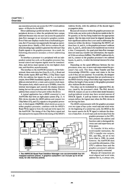
CHAPTER 1Overviewany execution process can access the CPU's total addressspace--4 Gbytes for the 68020.Direct addressing is preferred when the 68020 controlsperipheral devices or when the peripherals have uniqueaddresses because only one user can access the quad pixeldata-flow manager in an interactive graphics system.Even if this user displays results from a multitasking process,the I/O accesses run sequentially through an operatingsystem driver. Ideally, a PAL device contains the addressdecoding logic needed to generate the relevant ChipEnable signals to the graphics processor. As a result, thefollowing discussion assumes a direct-addressingscheme.To interface a processor to a peripheral with an independentsystem bus cycle, as the graphics processor has,several control and response signals must be translated.Also, each device must operate at its own highest clockrate, and therefore, asynchronously.The interface to the Am95C60 includes a 16-bit bidirectional,three-state data bus (lines Do to DIs), Read andWrite strobe inputs (RD and WR), a Chip Select input(CS), two address line inputs (Ao and AI)' an interruptoutput, three DMA handshake signals, an output that enablesan external driver, a reset, and a system clock input.The system clock, which runs at up to 20 MHz, times theinternal microengine and controls the display-memorytiming, but not the system-bus and video timing. The twoaddress lines connect to four ports within the device.A typical application has a 68020 connected to twoAm95C60s that form an eight-plane system (Fig. 2). APAL device decodes the 68020 address and outputs twoChip Select (CSo and CSI) signals to the graphics processors.A third signal, CSQPDM, which shows an access toeither graphics processor, combines with the 68020'sReadIWrite signal to form the read and write inputs forthe Am95C60. The timing of the Chip Select signal andthe read and write inputs follows the timing of the 68020'sSystem busRedGreenBlueColorpalette1. The AM95C60 Quad Pixel Datal/ow Manager can accommodate four bitmappedmemory planes. A graphics subsystem can include up to 64 devices,for 256 memory planes.Address Strobe, with the addition of the decode logic'Spropagation delay.Because all resources within the graphics processor are16 bits wide, any write cycle to the device results in the 16-bit quantity on the bus being loaded into the appropriateregister. But the data word must be aligned, because theleast significant address line is not used in addressing theresources within the device. Connecting the 68020's addresslines, Al and A2, to the graphics processor's addresspins, Ao and AI> allows data to be transferred one word ata time. Consequently, the quad pixel data-flow managerdoes not need any transfer-size information; the requested16 bits are always fulfilled. The 68020's address bits Aland A2 connect to the graphics processor's two addressinputs, Ao and AI' to select the internal resource for a busaccess.Depending on the speed difference between the twoprocessors, none, one, or more wait states extend the processor'sbus cycle. Two lines-Data Transfer and SizeAcknowledge (DSACK)-
- Page 1 and 2: Am95C60Quad Pixel Dataflow ManagerA
- Page 3 and 4: Authors:Tom CrawfordStuart TindallE
- Page 6: Table of ContentsCHAPTER 1 Overview
- Page 12 and 13: and the information is read in on t
- Page 14 and 15: CHAPTER 1Overviewservice. As with t
- Page 16: CHAPTER 2System Bus Interface2.1 Am
- Page 19 and 20: CHAPTER 2System Bus InterfaceT4 1W
- Page 21 and 22: CHAPTER 2System Bus InterfaceALE ~t
- Page 23 and 24: CHAPTER 2System Bus InterfaceDMAQPD
- Page 25 and 26: CHAPTER 2System Bus Interfacevee20
- Page 27 and 28: CHAPTER 2System Bus InterfaceMATOUT
- Page 29 and 30: CHAPTER 2System Bus InterfaceQPDM i
- Page 31 and 32: CHAPTER 2System Bus InterfaceJ01501
- Page 33 and 34: CHAPTER 2System Bus Interfacedresse
- Page 35 and 36: CHAPTER 2System Bus InterfaceCUPL v
- Page 37 and 38: CHAPTER 2System Bus InterfaceCUPL v
- Page 39 and 40: CHAPTER 2System Bus InterfaceCUPL v
- Page 41 and 42: CHAPTER 2System Bus InterfaceCUPL V
- Page 43 and 44: CHAPTER 2System Bus InterfaceCUPL v
- Page 45 and 46: CHAPTER 2System Bus Interface2.2 VM
- Page 47 and 48: CHAPTER 2System Bus InterfaceAs ano
- Page 49 and 50: CHAPTER 2System Bus InterfaceADDRBu
- Page 51 and 52: CHAPTER 2System Bus Interface2.3 68
- Page 53 and 54: CHAPTER 2System Bus InterfaceFCVA+3
- Page 55 and 56: CHAPTER 2System Bus InterfacesEaUEN
- Page 57 and 58: CHAPTER 2System Bus Interfacethat c
- Page 59 and 60:
CHAPTER 2System Bus InterfaceAs the
- Page 61 and 62:
CHAPTER 2System Bus InterfaceDecode
- Page 63 and 64:
CHAPTER 2System Bus InterfaceAppend
- Page 65 and 66:
CHAPTER 2System Bus Interface2.3.12
- Page 67 and 68:
CHAPTER 2System Bus InterfaceAPPEND
- Page 69 and 70:
CHAPTER 2System Bus InterfaceAPPEND
- Page 71 and 72:
CHAPTER 2System Bus InterfaceAPPEND
- Page 73 and 74:
CHAPTER 2System Bus InterfaceData i
- Page 76 and 77:
CHAPTER 3Display Memory BusIn this
- Page 78 and 79:
CHAPTER 3Display Memory BusTo minim
- Page 80 and 81:
CHAPTER 3Display Memory BusAOOA"(7;
- Page 82 and 83:
CHAPTER 3Display Memory BusFurtherm
- Page 84 and 85:
CHAPTER 3Display Memory BusTo run t
- Page 86 and 87:
CHAPTER 3Display Memory BusQPDM) as
- Page 88 and 89:
CHAPTER 3Display Memory BusCDAT -0
- Page 90 and 91:
CHAPTER 3Display Memory Busoutput b
- Page 92 and 93:
CHAPTER 3Display Memory BusDIM qpar
- Page 94 and 95:
CHAPTER 3Display Memory Busram.para
- Page 96 and 97:
DATA 99,99,10,20,99,99,99,99,99,tw(
- Page 98 and 99:
CHAPTER 3Display Memory BusDATA 5,-
- Page 100 and 101:
CHAPTER 3Display Memory BusGOSUB fi
- Page 102 and 103:
CHAPTER 3Display Memory Busramp=18:
- Page 104 and 105:
CHAPTER 3Display Memory BusGOSUB fi
- Page 106 and 107:
CHAPTER 3Display Memory Busramp=46:
- Page 108 and 109:
CHAPTER 3Display Memory Busparam69:
- Page 110 and 111:
amp=93 :GOSUB out.paramtext$="this
- Page 112 and 113:
CHAPTER 3Display Memory BusRETURNge
- Page 114 and 115:
CHAPTER 3Display Memory Bustext$="N
- Page 116 and 117:
CHAPTER 3Display Memory BusKANJI RO
- Page 118 and 119:
CHAPTER 3Display Memory BusTable 3.
- Page 120 and 121:
Al1 -1'01----.----------1lSI Level0
- Page 122:
CHAPTER 4Video Bus4.1 VIDEO BUS4.2
- Page 125 and 126:
CHAPTER 4Video Bus4.2.2 High-speed
- Page 127 and 128:
CHAPTER 4Video BusScan Line End Con
- Page 129 and 130:
CHAPTER 4Video BusFIFO (VDAF). The
- Page 131 and 132:
CHAPTER 4Video BusParameter min typ
- Page 134:
CHAPTER 5Evaluation and Demonstrati
- Page 137 and 138:
CHAPTER 5Evaluation and Demonstrati
- Page 139 and 140:
CHAPTER 5Evaluation and Demonstrati
- Page 141 and 142:
CHAPTER 5Evaluation and Demonstrati
- Page 143 and 144:
CHAPTER 5Evaluation and Demonstrati
- Page 145 and 146:
CHAPTERSEvaluation and Demonstratio
- Page 147 and 148:
CHAPTER 5Evaluation and Demonstrati
- Page 149 and 150:
CHAPTER 5Evaluatuion and Demonstrat
- Page 151 and 152:
CHAPTERSEvaluation and Demonstratio
- Page 153 and 154:
CHAPTERSEvaluation and Demonstratio
- Page 155 and 156:
CHAPTER 5Evaluation and Demonstrati
- Page 157 and 158:
CHAPTER 5Evaluation and Demonstrati
- Page 159 and 160:
C{I~P2-01 T22 T 22 TO. 1 41-44. 48-
- Page 161 and 162:
(JIN0>2D2PROM_(SA16: :~~~202
- Page 163 and 164:
(.TI~8A22828C26A7'A66A'6A37C77C6704
- Page 165 and 166:
c.nWo607, Be2 DClK2 » ============
- Page 168:
CHAPTER 6Articles/Application Notes
- Page 171 and 172:
CHAPTER 6Software10 'This programs
- Page 173 and 174:
CHAPTER 6Software950 RETURN960 '970
- Page 175 and 176:
CHAPTER 6Software6.2 COPY BLOCK OPE
- Page 177 and 178:
CHAPTER 6Software6.2.4 Transparency
- Page 179 and 180:
CHAPTER 6Softwarecpy 11 a [temp2] [
- Page 181 and 182:
CHAPTER 6Softwarecpy 11 a [temp2] [
- Page 183 and 184:
CHAPTER 6SoftwareADDTEMPblk [blksiz
- Page 185 and 186:
CHAPTER 6SoftWareSUBSTEMPblk [blksi
- Page 187 and 188:
NOTES
- Page 189 and 190:
NOTES
- Page 191 and 192:
NOTES
- Page 193:
ADVANCED MICRO DEVICES' NORTH AMERI