


You also want an ePaper? Increase the reach of your titles
YUMPU automatically turns print PDFs into web optimized ePapers that Google loves.
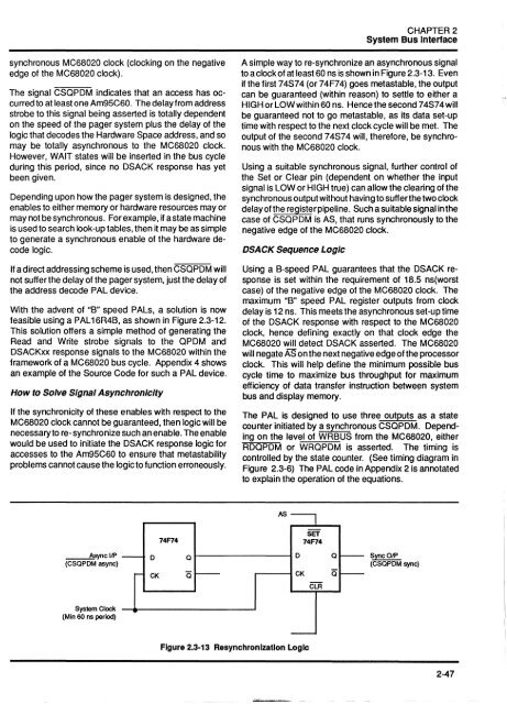
CHAPTER 2System Bus Interfacesynchronous MC68020 clock (clocking on the negativeedge of the MC68020 clock).The signal CSQPDM indicates that an access has occurredto at least one Am95C60. The delay from addressstrobe to this Signal being asserted is totally dependenton the speed of the pager system plus the delay of thelogic that decodes the Hardware Space address, and somay be totally asynchronous to the MC68020 clock.However, WAIT states will be inserted in the bus cycleduring this period, since no DSACK response has yetbeen given.Depending upon how the pager system is designed, theenables to either memory or hardware resources mayormay not be synchronous. For example, if a state machineis used to search look-up tables, then it may be as simpleto generate a synchronous enable of the hardware decodelogic.If a direct addressing scheme is used, then CSQPDM willnot suffer the delay of the pager system, just the delay ofthe address decode PAL device.With the advent of "8" speed PALs, a solution is nowfeasible using a PAL 16R48, as shown in Figure 2.3-12.This solution offers a simple method of generating theRead and Write strobe Signals to the QPDM andDSACKxx response signals to the MC68020 within theframework of a MC68020 bus cycle. Appendix 4 showsan example of the Source Code for such a PAL device.How to Solve Signal AsynchronlcltyIf the synchronicity of these enables with respect to theMC68020 clock cannot be guaranteed, then logic will benecessary to re- synchronize such an enable. The enablewould be used to initiate the DSACK response logic foraccesses to the Am95C60 to ensure that metastabilityproblems cannot cause the logic to function erroneously.A simple way to re-synchronize an asynchronous signalto a clock of at least 60 ns is shown in Figure 2.3-13. Evenif the first 74S74 (or 74F74) goes metastable, the outputcan be guaranteed (within reason) to settle to either aHIGH or LOWwithin 60 ns. Hence the second 7 4S7 4 willbe guaranteed not to go metastable, as its data set-uptime with respect to the next clock cycle will be met. Theoutput of the second 74S74 will, therefore, be synchronouswith the MC68020 clock.Using a suitable synchronous signal, further control ofthe Set or Clear pin (dependent on whether the inputsignal is LOW or HIGH true) can allow the clearing of thesynchronous output without having to suffer the two clockdelay of the register pipeline. Such a suitable signalinthecase of CSQPDM is AS, that runs synchronously to thenegative edge of the MC68020 clock.DSACK Sequence LogicUsing a 8-speed PAL guarantees that the DSACK responseis set within the requirement of 18.5 ns(worstcase) of the negative edge of the MC68020 clock. Themaximum "8" speed PAL register outputs from clockdelay is 12 ns. This meets the asynchronous set-up timeof the DSACK response with respect to the MC68020clock, hence defining exactly on that clock edge theMC68020 will detect DSACK asserted. The MC68020will negate AS on the next negative edge of the processorclock. This will help define the minimum possible buscycle time to maximize bus throughput for maximumefficiency of data transfer instruction between systembus and display memory.The PAL is designed to use three outputs as a statecounter initiated by a synchronous CSQPDM. Dependingon the level of WR8US from the MC68020, eitherRDQPDM or WRQPDM is asserted. The timing iscontrolled by the state counter. (See timing diagram inFigure 2.3-6) The PAL code in Appendix 2 is annotatedto explain the operation of the equations.___ Async lIP(CSQPDM async)74F74SET74F74o Q t--------; 0 Q SyncOIP(CSQPDM sync)CK.-----tCKSystem Clock -..------------'(Min 60 ns period)Figure 2.3-13 Resynchronlzation Logic2-47


