


You also want an ePaper? Increase the reach of your titles
YUMPU automatically turns print PDFs into web optimized ePapers that Google loves.
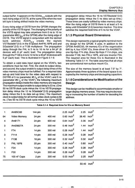
CHAPTER 3Display Memory Busoutput buffer. It appears on the SDrite 7 _ 0 outputs with thenext rising edge of DSTB, at the same time when the nextleft byte is being shifted inside the video memory.Every rising edge of DSTB from the QPDM changes thepolarity of the VSTB signal. The changing of the polarity ofthe VSTB signal may take anywhere from 0 ns to 10 ns(parameter #80 ~D of the QPDM) after the rising edge ofDSTB. This VSTB signal in conjunction with the latchedbank address ADDR 9 _ B create the signalsVSTBsidebk*(3:0) in the B-speed AmPAL18P8 and andSGsidebk*(3:0) in a F138 multiplexer. The propagationdelay through the PAL is 5 ns to 16 ns for a 64 pF (8devices with 8 pF each) load. The propagation delaythrough the F138 is4 ns to 12 ns for a40 pF (8 devices with5 pF each) load. This is illustrated in Figure 3.1-9.To obtain a valid data input signal on the VDAFs, twoconditions must be met. First, the clock-to-output delay,and second, the output enable to output delay times of thevideo memory chips must be fulfilled. For a required dataset-up and hold time for the video data with respect toDSTRB of 5 ns (parameter #5 ts of the VDAF) and 5 ns(parameter #6 tH of the VDAF), the following maximumpropagation delays inside the video memory are required.The maximum output enable to output delay is 23 ns. (One50 ns DSTB clock cycle minus the 10 ns VSTB propagationdelay minus the 12 ns SGsidebk*(3:0) propagationdelay minus the 5 ns data set-up time.) The maximumclock to output delay for all normal video clock cycles is 69ns. (Two 50 ns DSTB clock cycle minus the 10 ns VSTBpropagation delay minus the 16 ns VSTBsidebk*(3:0)propagation delay minus the 5 ns data set-up time.)These times are easily fulfilled by video memory chips.After the rising edge of DSTB there is at least a 5 nsdelay until SGsidebk*(3:0) becomes inactive. This timesatisfies the required hold time of 5 ns for the VDAF.3.1.5 Physical Board DimensionsThis design represents a typical graphic terminal memorydesign for the QPDM. It uses, in addition to theQPDM Am95C60, 64 memory ICs of the organization64K by 4, four VDAF ICs, three driver ICs Am28827 A,one flip-flop F74 chip, three flip-flops Fl14 chips, onedecoder F138, two PALs 18P8, and one inverter F04.The required area for these ICs is illustrated in thefollowing Table 3.1-4. The table assumes that all chipsare conventional non-surface mount ICs.The size of the memory board is at least 7.5" by 7".Approximately three-quarters of the board space is occupiedby the memory chips and decoupli ng capacitors.3.1.6 Considerations for Modification of theDesignThis design can be modified to accommodate smaller orlarger display memory areas. This may requiredecreasingor increasing the number of banks for decoding theaddress.Table 3.1-4 Required Area for ICs on Memory Board644Am95C60Video MemoryAm8171144 pin24 pin24 pin2.25 inch2 2.25 inch 2400 mil 0.60 inch 2 38.40 inch 2600 mil 0.84 inch 2 3.36 inch 23Am29827A24 pin300 mil 0.48 inch2 1.44 inch 23275F74Fl14F138PAL 18P8F04FOO100 nF Caps14 pin14 pin16 pin20 pin14 pin14 pin2 pin300 mil 0.28 inch 2 1.44 inch 2300 mil 0.28 inch 2 0.28 inch 2300 mil 0.32 inch 2 0.32 inch 2300 mil 0.40 inch 2 0.80 inch 2300 mil 0.28 inch 2 0.28 inch 2300 mil 0.28 inch 2 0.28 inch 2300 mil 0.03 inch 2 2.25 inch 250.40 inch 2 3·15


