Create successful ePaper yourself
Turn your PDF publications into a flip-book with our unique Google optimized e-Paper software.
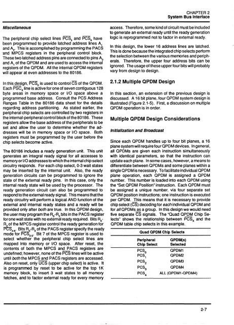
CHAPTER 2System Bus InterfaceMiscellaneousThe peripheral chip select lines PCSs and PCSs havebeen programmed to provide latched address lines A,and A2. This is accomplished by programming the PACS·and MPCS registers in the peripheral control block.These two latched address pins are connected to pins Aoand A, of the QPDM and are used to access the internalregisters of the QPDM. All the internal QPDM registerswill appear at even addresses to the 80186.In this design, PCSo is used to control CS of the QPDM.Each PSCx line is active for one of seven contiguous 128byte areas in memory space or 1/0 space above aprogrammed base address. Consult the PCS AddressRanges Table in the 80186 data sheet for the detailsregarding address partitioning. As stated earlier, theperipheral chip selects are controlled by two registers inthe internal-peripheral control block of the 80186. Theseregisters allow the base address of the peripherals to beset and allow the user to determine whether the addresseswill be in memory space or 1/0 space. Bothregisters must be programmed by the user before thechip selects become active.The 80186 includes a ready generation unit. This unitgenerates an integral ready signal for all accesses tomemory or 1/0 addresses to which the internal chip selectcircuitry responds. For each chip select, 0-3 wait statesmay be inserted by the internal unit. Also, the readygeneration circuits can be programmed to ignore thestate of the external ready pins. In this case, only theinternal ready state will be used by the processor. Theready generation circuit can also be programmed torespond to the external ready signal. This means that theready circuitry will perform a logical AND function of theexternal and internal ready states and a ready will beprovided only after both are true. In this QPDM design,the user may program the Ro-R2 bits in the PACS registerfor one wait state with no external ready required. Bits RoR2 of the MPCS register control the ready generation forf'CS 4 .jl. Bits Ro-R2 ofthe PACS register specify the readymode for PCS()'3. Bit 7 of the MPCS register is used toselect whether the peripheral chip select lines aremapped into memory or 1/0 space. After reset, thecontents of both the MPCS and PACS registers areundefined; however, none of the PCS lines will be activeuntil both the MPCS and PACS registers are accessed.Also on reset, only UCS (upper chip select) is active. Itis programmed by reset to be active for the top 1 Kmemory block, to insert 3 wait states to all memoryfetches, and to factor external ready for every memoryaccess. Therefore, some kind of circuit must be includedto generate an external ready until the ready generationlogic is reprogrammed not to factor in external ready.In this design, the lower 16 address lines are latched.This is done because the integrated chip selects performthe selection between the various memories and peripherals.Therefore, the upper four address bits can beignored. The usage of these upper four bits will probablyvary from design to design.2.1.2 Multiple QPDM DesignIn this section, an extension of the previous design isdiscussed. A 16 bit plane, four QPDM system design isillustrated (Figure 2.1-5). First, a discussion on multipleQPDM operation is in order.Multiple QPDM Design ConsiderationsInitialization and BroadcastSince each QPDM handles up to four bit planes, a 16plane system will require four QPDM devices. In general,all QPDMs are given each instruction simultaneouslywith identical parameters, so that the instruction canupdate each plane. In some cases, however, a means todifferentiate between QPDMs and some planes within asingle QPDM is necessary. To facilitate individual QPDMplane operation, each QPDM is assigned a QPDMnumber. This number is loaded into each QPDM usingthe "Set QPDM Position" instruction. Each QPDM mustbe assigned a unique number, via four separate setQPDM position instructions; one instruction is executedper QPDM. This means that it is necessary to providechip select (CS) decoding for each individual QPDM andfor al/ QPDMs as a group. In this design we would needfive separate CS signals. The "Quad QPDM Chip Selects"shows the relationship between PCSx and theQPDM table chip selects in this example.Quad QPDM Chip SelectsPeripheralChip SelectPCSoPCS,PCS 2PCS 3PCS 4QPDM(s)SelectedOPDM1OPDM2OPDM3OPDM4ALL (OPDM1-0PDM4)2-7


