


Create successful ePaper yourself
Turn your PDF publications into a flip-book with our unique Google optimized e-Paper software.
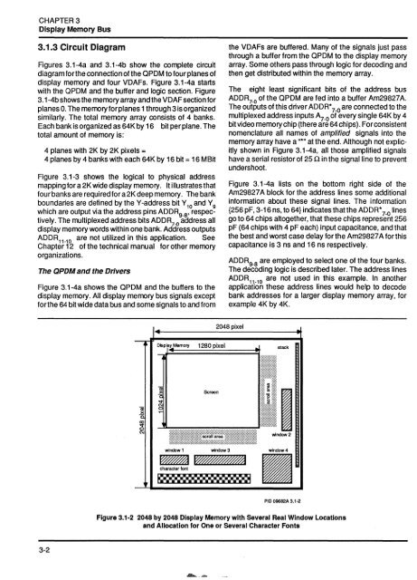
CHAPTER 3Display Memory Bus3.1.3 Circuit DiagramFigures 3.1-4a and 3.1-4b show the complete circuitdiagram iorthe connection of the QPDM to four planes ofdisplay memory and four VDAFs. Figure 3.1-4a startswith the QPDM and the buffer and logic section. Figure3.1-4b shows the memory array and the VDAF section forplanes O. The memory for planes 1 through 3 is organizedsimilarly. The total memory array consists of 4 banks.Each bank is organized as 64K by 16 bit per plane. Thetotal amount of memory is:4 planes with 2K by 2K pixels =4 planes by 4 banks with each 64K by 16 bit = 16 MBitFigure 3.1-3 shows the logical to physical addressmapping for a 2K wide display memory. It illustrates thatfour banks are required for a 2K deep memory. The bankboundaries are defined by the V-address bit Y 10 and Y 9which are output via the address pins ADDR 9 _ 8 , respectively.The multiplexed address bits ADDR .() address alldisplay memory words within one bank. Address outputsADDR 11 . 10 are not utilized in this application. SeeChapter 12 of the technical manual for other memoryorganizations.The QPDM and the DriversFigure 3.1-4a shows the QPDM and the buffers to thedisplay memory. All display memory bus signals exceptforthe 64 bit wide data bus and some signals to and fromthe VDAFs are buffered. Many of the signals just passthrough a buffer from the QPDM to the display memoryarray. Some others pass through logic for decoding andthen get distributed within the memory array.The eight least significant bits of the address busADDR 7 . 0 of the QPDM are fed into a buffer Am29827A.The outputs of this driver ADDR* 7-0 are connected to themultiplexed address inputs A 7 _ 0 of every single 64K by 4bit video memory chip (there are 64 chips). Forconsistentnomenclature all names of amplified signals into thememory array have a "*,, at the end. Although not explicitlyshown in Figure 3.1-4a, all those amplified signalshave a serial resistor of 25 n in the signal line to preventundershoot.Figure 3.1-4a lists on the bottom right side of theAm29827 A block for the address lines some additionalinformation about these signal lines. The information{256 pF, 3-16 ns, to 64} indicates that the ADDR* 7-0 linesgo to 64 chips altogether, that these chips represent 256pF (64 chips with 4 pF each) input capacitance, and thatthe best and worst case delay for the Am29827 A for thiscapacitance is 3 ns and 16 ns respectively.ADDR 9 _ 8 are employed to select one of the four banks.The decoding logic is described later. The address linesADDR 11 . 10 are not used in this example. In anotherapplication these address lines would help to decodebank addresses for a larger display memory array, forexample 4K by 4K.2048 pixelstackwindow 1 window 3JM%l?iJ~character fontF»»»»»»»PID 09682A 3.1-2Figure 3.1-2 2048 by 2048 Display Memory with Several Real Window Locationsand Allocation for One or Several Character Fonts3-2


