You also want an ePaper? Increase the reach of your titles
YUMPU automatically turns print PDFs into web optimized ePapers that Google loves.
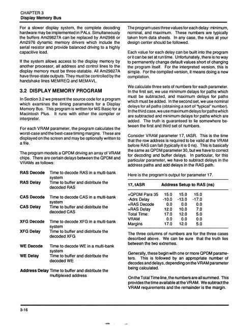
-- -CHAPTER 3Display Memory BusFor a slower display system, the complete decodinghardware may be implemented in PALs. SimuHaneouslythe buffers Am29827 A can be replaced by Am2966 orAm2976 dynamic memory drivers which include theserial resistor and provide balanced driving to a highlycapacitive load.If the system allows access to the display memory byanother processor, all address and control lines to thedisplay memory must be three-statable. All Am29827Ahave three-state outputs. They must be controlled by thehandshake lines MEMREO and MEMAVL.3.2 DISPLAY MEMORY PROGRAMIn Section 3.2 we present the source code for a programwhich examines the timing parameters for a DisplayMemory Bus. This program is written for MS Basic for aMacintosh Plus. It runs with either the compiler orinterpreter.For each VRAM parameter, the program calculates theworst-case and the best-case timing margins. These aredisplayed on the screen and may be optionally written toa file.The program models a OPDM driving an array of VRAMchips. There are certain delays between the OPDM andVRAMs as follows:RAS DecodeRAS DelayCAS DecodeCAS DelayXFG DecodeXFG DelayWE DecodeWE DelayTime to decode RAS in a muHi-banksystemTime to buffer and distribute thedecoded RASTime to decode CAS in a muHi-banksystemTime to buffer and distribute thedecoded CASTime to decode XFG in a muHi-banksystemTime to buffer and distribute thedecodedXFGTime to decode WE in a muHi-banksystemTime to buffer and distribute thedecoded WEAddress Delay Time to buffer and distribute themuHiplexed addressThe program !Jses three values for each delay: minimum,nominal, and maximum. These numbers are typicallytaken from data sheets. In any case, the rules at yourdesign center should be followed.Each value for each delay can be built into the programor it can be set at run time. Unfortunately, there is no wayto permanently change defauH values short of changingthe program itself. For the interpreted version, this issimple. Forthe compiled version, it means doing a newcompilation.We calculate three sets of numbers for each parameter.In the first set, we use minimum delays for paths whichmust be subtracted, and maximum delays for pathswhich must be added. In the second set, we use nominaldelays for all paths (obtaining a sort of "ypical" number).In the third case, we use maximum delays for paths whichare subtracted and minimum delays for paths which areadded. The truth is guaranteed to lie somewhere betweenthe first and third set of numbers.Consider VRAM parameter 17, tASR. This is the timethat the row address is required to be valid at the VRAMbefore RAS can fall (typically it is 0 ns). This is basicallythe same as OPDM parameter 30, but we have to correctfor decoding and buffer delays. In particular, for thisparticular parameter, we have to subtract delays in theaddress paths and add delays in the RASpath.Here is the program's output for parameter 17.17,tASRAddress Setup to RAS (ns)+OPDM Para 35 15.0 15.0 15.0-Adrs Delay -10.0 -13.0 -17.0+RAS Decode 0.0 0.0 0.0+RAS Delay 12.0 10.0 7.0Total Time: 17.0 12.0 5.0VRAM 0.0 0.0 0.0Margins 17.0 12.0 5.0The three columns of numbers are for the three casesdescribed above. We can be sure that the truth liesbetween the two extremes.Generally, these begin with one or more OPDM parameters.This is followed by an appropriate number ofdecodes and delays, depending onthe VRAM parameterbeing calculated.Onthe Total Time line, the numbers are all summed. Thisprovides the time available at the VRAM. We subtract theVRAM requirements and the remainder is the margin.3-16


