CHAPTER 2System Bus InterfaceThe MC68020 Interrupt SequenceThe interrupt sequence of the MC68020 is as follows:The MC68020 monitors the level of the IPL0-2 lines.When a non-zero level is detected for at least twoconsecutive system clocks, the MC68020 internally flagsthat a genuine external interrupt condition exists. Notethat the IPL0-2 lines are active LOW.If this interrupt level present on the the IPL0-2 lines isgreater than the current interrupt level, this will cause thehost processor to "stack" the state of the machine oncompletion of the current instruction. The MC68020 willthen generate an Interrupt Acknowledge (Read) BusCycle (lACK cycle) to determine which interrupting devicefor any particular interrupt level has raised theinterrupt. The device with an interrupt pending canrespond to this bus cycle by supplying a vector numberthat is used to index into an Interrupt Address table topoint to a unique program subroutine to service thatparticular interrupt.Using AutovectorsIt is not essential that the interrupting device respond tothis lACK cycle by providing a vector number and generatinga DSACK response as previously described. Instead,the device can cause the AVEC line to be assertedto the MC68020, indicating that the Autovector for thisparticular interrupt level should be used. Within theVector Address table, this causes a specific entry uniquefor each interrupt level, to be used as the source of theinterrupt service routine start address, instead of usingthe returned vector number to index into the VectorAddress table to provide this start address.Using the Autovector system to respond to the lACKcycle, caused by the Am95C60 interrupt, makes thehardware support more simple, as the Am95C60 doesnot have a specific on-board register to hold an interruptvector number. However, should a particular systemrequire it, it would be relatively simple to use an externalregister to hold the vector number enabled by a suitablesignal from the "Hardware Space" decode logic. Whenusing the Autovector feature, the Am95C60 does notneed to be informed that the lACK cycle has occurred atthis time, but decode logic can set the AVEC line to theMC68020 in response to the lACK cycle. (SeeFigure 2.3-11)On entering the interrupt service routine for theAm95C60, the software should read the Status Registerof the Am95C60. From this register the software candetermine that interrupt conditions currently require service.To clear the relevant bits within the Am95C60, aWrite to the Interrupt Acknowledge Register should beissued defining that bits of the Interrupt Register are to bereset. If no further interrupt conditions have become setsince reading the Status Register, this Write to theInterrupt Acknowledge Register will cause the interruptline from the Am95C60 to be negated.If, after the Status Register has been read to determineoutstanding interrupts, another interrupt condition occursbefore the Write Interrupt Register occurs, then thisnewly set bit will not be cleared by the Write to theInterrupt Acknowledge Register, and hence the interruptline will not be reset. This does not cause a problem,however, since when the interrupt routine completes andtries to return to the previous interrupt level, theMC68020 will again be interrupted due to this newinterrupt condition. The interrupt routine will again beentered, allowing this new bit to be read, cleared andserviced. This mechanism guarantees that no interruptwill be lost.Note that if an lACK cycle occurs but the interruptcondition causing the lACK cycle to be generated by theMC68020 is no longer set, then a Spurious Interrupt hasoccurred. Under this circumstance, the lACK cycleshould be responded to with Bus Error, not DSACKxx orAVEC. The MC68020 will interpret the Bus Error signalto indicate that the Spurious Interrupt vector should beused as the entry address into an interrupt routine. TheMC68020 will not take the Bus Error exception.Reading the Status RegisterWhen reading the Status Register of an Am95C60, thedevice must be explicitly addressed using the uniqueaddress associated with that Am95C60, as used whensetting the Plane Position Register of each Am95C60. Ifthe global address is used, multiple devices will attemptto drive the system bus simuHaneously. All QPDMs will,however, contain the same value in their StatusRegisters.System Interrupt PriorityTo prioritize a number of interrupts, some of which maycause the same interrupt level, a PAL device may beused simply to look at the currently outstanding interrupts.The relevant interrupt level can than be assertedon the IPLo.2 lines to the MC68020. All devices must holdtheir interrupt lines asserted until the device receives anappropriate Acknowledge to their interrupt. Those devicesthat can return an Interrupt Vector should have anindividual lACK line asserted to them during the lACKcycle, informing the device to return the vector number.Again, a PAL device can be used to generate the individuallACKlines, assuring that only one device responds toany lACK cycle. (See Figure 2.3-11).--2-45
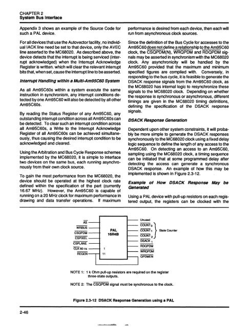
CHAPTER 2System Bus InterfaceAppendix 3 shows an example of the Source Code forsuch a PAL device.For all devices that use the Autovector facility, no individuallACKline need be set to that device, only the AVECline asserted to the MC68020. As described above, thedevice detects that the interrupt is being serviced (interruptacknowledged) when the Interrupt AcknowledgeRegister is written. which will clear the relevant interruptbits that, when set, cause the interrupt line to be asserted.Interrupt Handling within a Multi-Am95C60 SystemAs all Am95C60s within a system execute the sameinstruction in synchronism, any interrupt conditions detectedby one Am95C60 will also be detected by all otherAm95C60s.By reading the Status Register of any Am95C60, anyoutstanding interrupt condition across all Am95C60s canbe detected. To clear such an interrupt condition acrossall Am95C60s, a Write to the Interrupt AcknowledgeRegister of all Am95C60s can be achieved simultaneously,thus ca\Jsing the desired interrupt condition to beacknowledged and cleared.Using the Arbitration and Bus Cycle Response schemesimplemented by the MC68020, it is simple to interfacetwo devices on the same bus, each running asynchronouslyfrom their own clock source.To gain the most performance from the MC68020, thedevice should be operated at the highest clock ratedefined within the specification of the part (currently16.67 MHz). However, the Ann95C60 is capable ofrunning on a 20 MHz clock for maximum performance indrawing and data transfer operations. If maximumperformance is desired from each device, then each willrun from asynchronous clock sources.Since the definition of the Bus Cycle for accesses to theAm95C60 does not define a relationship to the Am95C60clock, the CSQPDM(N), WRQPDM and RDQPDM signalsmay be asserted in synchronism with the MC68020clock. Any asynchronicity will be handled by theAm95C60 provided that the maximum and minimumspecified figures are complied with. Conversely, inresponding to the bus cycle, it is feasible to generate theDSACK response signals from the Am95C60 clock, asthe MC68020 has internal logic to resynchronize thesesignals to the MC68020 clock. Depending on whetherthe response is synchronous or asynchronous, differenttimings are given in the MC68020 timing definitions,defining the specification of the DSACK responsesignals.DSACK Response GenerationDependent upon other system constraints, it will probablybe more simple to generate the DSACK responsessynchronously to the MC68020 clock using a fixed delaylogic sequence to define the length of any access to theAm95C60. On detecting an access to an Am95C60,sampling using the MC68020 clock, a timing sequencecan be initiated that at some programmed delay afterdetecting the access can generate a synchronousDSACK response. An example of how this may beimplemented is shown in Figure 2.3-12.Example of How DSACK Response May beGeneratedUsing a PAL device with pull-up resistors on each registeredoutput, the registers can be clocked with theASWRBUSCSOPDMCSPiXELCSPl.ANECLK60 nsREGEN 11PAL16R4BUnused=:; ~} State CounterCOUNT 2DSACK 1RDOPDMWROPDMQPDMENNOTE 1: 1 k Ohm pull-up resistors are required on the registerthree-state outputs.NOTE 2: The CSQPDM signal must be synchronous to the clock.Figure 2.3-12 DSACK Response Generation using a PAL2-46
- Page 1 and 2:
Am95C60Quad Pixel Dataflow ManagerA
- Page 3 and 4:
Authors:Tom CrawfordStuart TindallE
- Page 6:
Table of ContentsCHAPTER 1 Overview
- Page 10 and 11:
CHAPTER 1OverviewDESIGN APPLICATION
- Page 12 and 13: and the information is read in on t
- Page 14 and 15: CHAPTER 1Overviewservice. As with t
- Page 16: CHAPTER 2System Bus Interface2.1 Am
- Page 19 and 20: CHAPTER 2System Bus InterfaceT4 1W
- Page 21 and 22: CHAPTER 2System Bus InterfaceALE ~t
- Page 23 and 24: CHAPTER 2System Bus InterfaceDMAQPD
- Page 25 and 26: CHAPTER 2System Bus Interfacevee20
- Page 27 and 28: CHAPTER 2System Bus InterfaceMATOUT
- Page 29 and 30: CHAPTER 2System Bus InterfaceQPDM i
- Page 31 and 32: CHAPTER 2System Bus InterfaceJ01501
- Page 33 and 34: CHAPTER 2System Bus Interfacedresse
- Page 35 and 36: CHAPTER 2System Bus InterfaceCUPL v
- Page 37 and 38: CHAPTER 2System Bus InterfaceCUPL v
- Page 39 and 40: CHAPTER 2System Bus InterfaceCUPL v
- Page 41 and 42: CHAPTER 2System Bus InterfaceCUPL V
- Page 43 and 44: CHAPTER 2System Bus InterfaceCUPL v
- Page 45 and 46: CHAPTER 2System Bus Interface2.2 VM
- Page 47 and 48: CHAPTER 2System Bus InterfaceAs ano
- Page 49 and 50: CHAPTER 2System Bus InterfaceADDRBu
- Page 51 and 52: CHAPTER 2System Bus Interface2.3 68
- Page 53 and 54: CHAPTER 2System Bus InterfaceFCVA+3
- Page 55 and 56: CHAPTER 2System Bus InterfacesEaUEN
- Page 57 and 58: CHAPTER 2System Bus Interfacethat c
- Page 59 and 60: CHAPTER 2System Bus InterfaceAs the
- Page 61: CHAPTER 2System Bus InterfaceDecode
- Page 65 and 66: CHAPTER 2System Bus Interface2.3.12
- Page 67 and 68: CHAPTER 2System Bus InterfaceAPPEND
- Page 69 and 70: CHAPTER 2System Bus InterfaceAPPEND
- Page 71 and 72: CHAPTER 2System Bus InterfaceAPPEND
- Page 73 and 74: CHAPTER 2System Bus InterfaceData i
- Page 76 and 77: CHAPTER 3Display Memory BusIn this
- Page 78 and 79: CHAPTER 3Display Memory BusTo minim
- Page 80 and 81: CHAPTER 3Display Memory BusAOOA"(7;
- Page 82 and 83: CHAPTER 3Display Memory BusFurtherm
- Page 84 and 85: CHAPTER 3Display Memory BusTo run t
- Page 86 and 87: CHAPTER 3Display Memory BusQPDM) as
- Page 88 and 89: CHAPTER 3Display Memory BusCDAT -0
- Page 90 and 91: CHAPTER 3Display Memory Busoutput b
- Page 92 and 93: CHAPTER 3Display Memory BusDIM qpar
- Page 94 and 95: CHAPTER 3Display Memory Busram.para
- Page 96 and 97: DATA 99,99,10,20,99,99,99,99,99,tw(
- Page 98 and 99: CHAPTER 3Display Memory BusDATA 5,-
- Page 100 and 101: CHAPTER 3Display Memory BusGOSUB fi
- Page 102 and 103: CHAPTER 3Display Memory Busramp=18:
- Page 104 and 105: CHAPTER 3Display Memory BusGOSUB fi
- Page 106 and 107: CHAPTER 3Display Memory Busramp=46:
- Page 108 and 109: CHAPTER 3Display Memory Busparam69:
- Page 110 and 111: amp=93 :GOSUB out.paramtext$="this
- Page 112 and 113:
CHAPTER 3Display Memory BusRETURNge
- Page 114 and 115:
CHAPTER 3Display Memory Bustext$="N
- Page 116 and 117:
CHAPTER 3Display Memory BusKANJI RO
- Page 118 and 119:
CHAPTER 3Display Memory BusTable 3.
- Page 120 and 121:
Al1 -1'01----.----------1lSI Level0
- Page 122:
CHAPTER 4Video Bus4.1 VIDEO BUS4.2
- Page 125 and 126:
CHAPTER 4Video Bus4.2.2 High-speed
- Page 127 and 128:
CHAPTER 4Video BusScan Line End Con
- Page 129 and 130:
CHAPTER 4Video BusFIFO (VDAF). The
- Page 131 and 132:
CHAPTER 4Video BusParameter min typ
- Page 134:
CHAPTER 5Evaluation and Demonstrati
- Page 137 and 138:
CHAPTER 5Evaluation and Demonstrati
- Page 139 and 140:
CHAPTER 5Evaluation and Demonstrati
- Page 141 and 142:
CHAPTER 5Evaluation and Demonstrati
- Page 143 and 144:
CHAPTER 5Evaluation and Demonstrati
- Page 145 and 146:
CHAPTERSEvaluation and Demonstratio
- Page 147 and 148:
CHAPTER 5Evaluation and Demonstrati
- Page 149 and 150:
CHAPTER 5Evaluatuion and Demonstrat
- Page 151 and 152:
CHAPTERSEvaluation and Demonstratio
- Page 153 and 154:
CHAPTERSEvaluation and Demonstratio
- Page 155 and 156:
CHAPTER 5Evaluation and Demonstrati
- Page 157 and 158:
CHAPTER 5Evaluation and Demonstrati
- Page 159 and 160:
C{I~P2-01 T22 T 22 TO. 1 41-44. 48-
- Page 161 and 162:
(JIN0>2D2PROM_(SA16: :~~~202
- Page 163 and 164:
(.TI~8A22828C26A7'A66A'6A37C77C6704
- Page 165 and 166:
c.nWo607, Be2 DClK2 » ============
- Page 168:
CHAPTER 6Articles/Application Notes
- Page 171 and 172:
CHAPTER 6Software10 'This programs
- Page 173 and 174:
CHAPTER 6Software950 RETURN960 '970
- Page 175 and 176:
CHAPTER 6Software6.2 COPY BLOCK OPE
- Page 177 and 178:
CHAPTER 6Software6.2.4 Transparency
- Page 179 and 180:
CHAPTER 6Softwarecpy 11 a [temp2] [
- Page 181 and 182:
CHAPTER 6Softwarecpy 11 a [temp2] [
- Page 183 and 184:
CHAPTER 6SoftwareADDTEMPblk [blksiz
- Page 185 and 186:
CHAPTER 6SoftWareSUBSTEMPblk [blksi
- Page 187 and 188:
NOTES
- Page 189 and 190:
NOTES
- Page 191 and 192:
NOTES
- Page 193:
ADVANCED MICRO DEVICES' NORTH AMERI