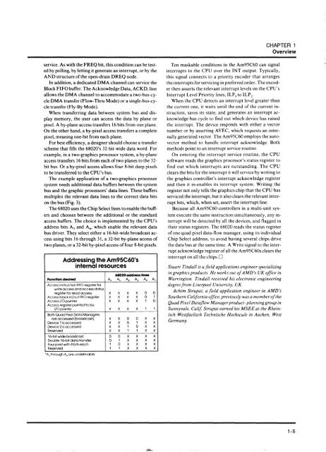
CHAPTER 1Overviewservice. As with the FREQ bit, this condition can be testedby polling, by letting it generate an interrupt, or by theAND structure of the open-drain DREQ node.In addition, a dedicated DMA channel can service theBlock FIFO butTer. The Acknowledge Data, ACKD, lineallows the DMA channel to accommodate a two-bus-cycleDMA transfer (Flow-Thru Mode) or a single-bus-cycletransfer (Fly-By Mode).When transferring data between system bus and displaymemory, the user can access the data by plane orpixel. A by-plane access transfers 16 bits from one plane.On the other hand, a by-pixel access transfers a completepixel, meaning one-bit from each plane.For best efficiency, a designer should choose a transferscheme that fills the 68020's 32-bit-wide data word. Forexample, in a two-graphics processor system, a by-planeaccess transfers 16 bits from each of two planes to the 32-bit bus. Or a by-pixel access allows four 8-bit deep pixelsto be transferred to the CPU's bus.The example application of a two-graphics processorsystem needs additional data butTers between the systembus and the graphic processors' data lines. These butTersmultiplex the relevant data lines to the correct data bitson the bus (Fig. 3).The 68020 uses the Chip Select lines to enable the butTersand chooses between the additional or the standardaccess butTers. The choice is implemented by the CPU'saddress bits As and A., which enable the relevant databus driver. They select either a l6-bit-wide broadcast accessusing bits 16 through 31, a 32-bit by-plane access oftwo planes, or a 32-bit by-pixel access offour 8-bit pixels.Addressing the Am95C60'sinternal resources68020 address linesfunction desired A. A, A, A, A, A,Access instruction FIFO register forwrite access and access statusregister for read access X X X X a aAccess block In/out FIFO register X X X X a 1Access I/O pointer X X X X 1 aAccess register pointed to byIjOpointer X X X X 1 1Both Quod Pixel Data Managersore accessed (broadcast) X X a a X XDevice 1 is accessed X X a 1 X XDevice 2 is accessed X X 1 a X XReserved X X 1 1 X X16-bit wide broadcast a a X X X XDouble 16-bit data transfer a 1 X X X XFour pixel with 8 bits each 1 a X X X XReserved 1 1 X X X XAJ through At, ore undefinableTen maskable conditions in the Am95C60 can signalinterrupts to the CPU over the INT output. Typically,this signal connects to a priority encoder that arrangesthe interrupts for servicing in preferred order. The encoderthen asserts the relevant interrupt levels on the CPU'sInterrupt Level Priority lines, ILP" to ILP ,.When the CPU detects an interrupt level greater thanthe current one, it waits until the end of the current instruction,saves its state, and generates an interrupt acknowledgebus cycle to find out which device has raisedthe interrupt. The device responds with either a vectornumber or by asserting AVEC, which requests an internallygenerated vector. The Am95C60 employs the autovectormethod to handle interrupt acknowledge. Bothmethods point to an interrupt service routine.On entering the interrupt service routine, the CPUsoftware reads the graphics processor's status register tofind out which interrupts are outstanding. The CPUclears the bits for the interrupt it will service by writing tothe graphics controller's interrupt acknowledge registerand then it re-enables its interrupt system. Writing theregister not only tells the graphics chip that the CPU hasserviced the interrupt, but it also clears the relevant interruptbits, which, when set, assert the interrupt line.Because all Am95C60 controllers in a multi-unit systemexecute the same instruction simultaneously, any interruptwill be detected by all the devices, and flagged intheir status registers. The 68020 reads the status registerof one quad pixel data-flow manager, using its individualChip Select address, to avoid having several chips drivethe data bus at the same time. A Write signal to the interruptacknowledge register of all the Am95C60s clears theinterrupt on all the chips. 0Stuart Tindall is a field applications engineer specializingin graphics products. He works out of AMD's UK office inWarrington. Tindall received his electronic engineeringdegree from Liverpool University, UK.Achim Strupat, a field application engineer in AMD'sSouthern Calzfornia office, previously was a member of theQuad Pixel Dataf/ow Manager product- planning group inSunnyvale, Calif Strupat earned his MSEE at the RheinischWestfaelisch Technische Hochscule in Aachen, WestGermany.1-5
CHAPTER 1Overview0(0:15)---------- ---WE (In)RAS, CASWIG~===;-(K)~ :::~O:~11)TSYNINMEMAVlMEMREa~MATOUTMAliNDMO(O:15)DM3 (015).. VSTBDSTBCOAT (0.2)~ __ ~--- FULLHRESET"-__ -1+--- ~~~~~TEVENThe 'our main functional blocks 01 /he Am95C60 are (he micro englfle systemInterface, display memory control/PI and vl(ieo IrmlflQ ('on/loUerGraphics controllerdraws 110,000 lines/secControls four bit-mappedmemory planesKA WAI UTI'\(;ivention is program mode, which letsyou store program data, pointer, andstack values alongside the displayablescreeI"'.The display-memory controller alsohas a data-plane controller, whichcontains four 16-bit data-logic umtsand four 16-bit bidirectional barrelshifter"The last mam functIOnal block IS thevideo-timing controller. which generatestiming SIgnals to control thevideo monitor and data transmi"siunon the video bus. Twelve video-controlregisters define honzontal timings,vertical timings, and operatingmode. You can program the 95(;60 tobe the honzontal master or slaw{s)and the vertical master or slave(s) ofanother video source in the system .Block copyOne of the 95C60's most useful capabilitiesis block ("opy. Operating atSO-nsec/pixel, thp chip moves largeI blocks of data ".,. ithin the hIt map.allowing source and destination overlapswithout cont~ntion or loss ofdata.During block copy, source data canbe rotated in 90" increments, mIrrored.and zoomed independently inX and Y dIrections. You can performlogical operations to the source pixelbefore it is written to the destinationBecause the 95C6'O supports maskwrite in video RAMs, the user canpreserve data integrity in selectedmemory planes during memory accesses.The block-copy feature also supportsone hardware window and manysoftware windows. Unlike softwarewindows, the hardware window doesnot overwrite the image it replaces.When using multiplE' windows. youean designate the most frequentlyus{'d window as the hardware windowand all remaining windows as softwarewindows. The 95C60 respondsrapidly to window movements by alteringpointers instead of bit-mapcontents.In addition to windowing, the chipsupports pannlllg, scrolling. andzoomlllg of graphiCS primitives drawnin various line styles. The 9;)C60 u::;esan antialiaslllg scheme that smoothsout the jagged edges of lines, arcs,and circlE'S by illuminating adjacentpixelsOther 95C60 capabliities includesupport of proportional spacing andfonts as large as 6;{x60 pixels---aOtimes larger than the 9x 14-pixel characterfont of an IBM PC. This largefont capability allows the chip to sup·port such foreign-language charactersets as Kanji. which r('quirc:-. 24x24pixels to produce Japanese eharacters.Tht, 95C60 comes in a 144-pin pingnd-arraypackage. PricE'S are$19H.57 for the 12-MHz version. $250for the Hi-MHz unit, and $27K.57 for a20-MHz device (00). Productionquantities are avaIlable now; delivery,four to six weeks ARO. 0theThe chip':, four In-bit data unit"\\ork 1Il parallel, oheying- in"tructiul\"that are de('o(\ed ano executf'd in aHi-bit micro l'ng-me with ainc:tructwll tIme. In add1t1011,archit('cturt' leb you ca:-:cade a,; many2:JIi-rnf-'mory-no dt'grariatioll lI'as 64 9;,('60,; toplan£' ,;ystem:-;performance.Graphics primitiwsTo speed execution, the dev]('!' Uq',hard-... irNI graphics algorithms tl) reduct'thl;' number of instruction,; a,;,;ociatedwith pach operatIOn. In COIltrast,a programmablf' graphic,;processor rf'quires the u,;pr to havt' adetailed kno\\ledge of It,; intt'rnal architecturean(1 to ,;pend time developingsoftware.The 95C60's instruction set supportsthe Implementation of suchgraphICS standards as ComputerGraphics Interface (CGl), GraphicalKernel System (GKS), and GraphicsDevice Interfacf' (GDl). A miero engine handles instruction eXl;'cution.Functional blocksThe micro engine, onl;' of four mainfunctional blocks on the chip, uses aathat nm lw t't'l"IJIlfigul"l'd toto all K· or Hi-bItho,;t prol"P,;,;or. mimmize the loadon the ho,;t, adp(licated OMA (·untrolll;'r("an be used to manag-.. data mO\Tmf'nt.During- J)!\1A UI)t'rations. th(· H'-l("l,I)uses a li4-\\or(]-dpt'p in,;trUl"twnFIFO buffer oppratmg" in flo\\thl'Ough mod(' to minimlzf' CIT \\ ait,;during instrUctIOn tran,;fprs. In additIOn,block-in and block-out buffer,;,;pf'P(1 data transfer from systf'mmemory to the display memory.The,;e block buffer,; ust' .. it her flowthroughor fly-by DMA.The third functional block-the display-memorycontrol1er-gelwratesdisplay-memory timing and arbitratE'Svidpo refreshes, memory refreshes,and updatl' a('cessps. To avoid \·ideoand update contentions for the displaymemories, the 950iO supports(iual-port vid('o RAMs.Video RAMsVideo RAMs improve the updatingof graphie~ memory by more than fivetimes over standard dynamic RAMs,Using video RAMs lets the chip refresha 12HOx 1024-piwl screen at fiOHz nonintE'rlaced. which translatesinto a I:~O-MHz pixel rate with morethan 90'7, of the time available fordisplay update.Another part of the display-memorycontroller is a translator that let~the CPU use X;Y coordinates forbackground and window locations.This frees the CPU from having toconvert X/Y screen coordinates todisplay-memory locations. An additionalfeature that reduces CPU inter-BEHIND THE DESIGNBit-map designcalled for videoRAMsAMD started designing theAm95C60 at the beginning of 1982·in response to increasing demandfor bit-mapped, high-resolutiontext and graphics displays. Theobjective was to build a high-perfonnancegraphics controllerbased on the company's bit~slicearchitecture.The bit-slice approach lets thedesigner increase data width bycascading multiple bit-slice processors.In the 95C60, the pixelwidth (color resolution) can be increasedby cascading 95C60s---onefor every four bit planes-withoutsacrificing drawing performance.One of the biggest design challengeswas keeping the die size
- Page 1 and 2: Am95C60Quad Pixel Dataflow ManagerA
- Page 3 and 4: Authors:Tom CrawfordStuart TindallE
- Page 6: Table of ContentsCHAPTER 1 Overview
- Page 10 and 11: CHAPTER 1OverviewDESIGN APPLICATION
- Page 12 and 13: and the information is read in on t
- Page 16: CHAPTER 2System Bus Interface2.1 Am
- Page 19 and 20: CHAPTER 2System Bus InterfaceT4 1W
- Page 21 and 22: CHAPTER 2System Bus InterfaceALE ~t
- Page 23 and 24: CHAPTER 2System Bus InterfaceDMAQPD
- Page 25 and 26: CHAPTER 2System Bus Interfacevee20
- Page 27 and 28: CHAPTER 2System Bus InterfaceMATOUT
- Page 29 and 30: CHAPTER 2System Bus InterfaceQPDM i
- Page 31 and 32: CHAPTER 2System Bus InterfaceJ01501
- Page 33 and 34: CHAPTER 2System Bus Interfacedresse
- Page 35 and 36: CHAPTER 2System Bus InterfaceCUPL v
- Page 37 and 38: CHAPTER 2System Bus InterfaceCUPL v
- Page 39 and 40: CHAPTER 2System Bus InterfaceCUPL v
- Page 41 and 42: CHAPTER 2System Bus InterfaceCUPL V
- Page 43 and 44: CHAPTER 2System Bus InterfaceCUPL v
- Page 45 and 46: CHAPTER 2System Bus Interface2.2 VM
- Page 47 and 48: CHAPTER 2System Bus InterfaceAs ano
- Page 49 and 50: CHAPTER 2System Bus InterfaceADDRBu
- Page 51 and 52: CHAPTER 2System Bus Interface2.3 68
- Page 53 and 54: CHAPTER 2System Bus InterfaceFCVA+3
- Page 55 and 56: CHAPTER 2System Bus InterfacesEaUEN
- Page 57 and 58: CHAPTER 2System Bus Interfacethat c
- Page 59 and 60: CHAPTER 2System Bus InterfaceAs the
- Page 61 and 62: CHAPTER 2System Bus InterfaceDecode
- Page 63 and 64: CHAPTER 2System Bus InterfaceAppend
- Page 65 and 66:
CHAPTER 2System Bus Interface2.3.12
- Page 67 and 68:
CHAPTER 2System Bus InterfaceAPPEND
- Page 69 and 70:
CHAPTER 2System Bus InterfaceAPPEND
- Page 71 and 72:
CHAPTER 2System Bus InterfaceAPPEND
- Page 73 and 74:
CHAPTER 2System Bus InterfaceData i
- Page 76 and 77:
CHAPTER 3Display Memory BusIn this
- Page 78 and 79:
CHAPTER 3Display Memory BusTo minim
- Page 80 and 81:
CHAPTER 3Display Memory BusAOOA"(7;
- Page 82 and 83:
CHAPTER 3Display Memory BusFurtherm
- Page 84 and 85:
CHAPTER 3Display Memory BusTo run t
- Page 86 and 87:
CHAPTER 3Display Memory BusQPDM) as
- Page 88 and 89:
CHAPTER 3Display Memory BusCDAT -0
- Page 90 and 91:
CHAPTER 3Display Memory Busoutput b
- Page 92 and 93:
CHAPTER 3Display Memory BusDIM qpar
- Page 94 and 95:
CHAPTER 3Display Memory Busram.para
- Page 96 and 97:
DATA 99,99,10,20,99,99,99,99,99,tw(
- Page 98 and 99:
CHAPTER 3Display Memory BusDATA 5,-
- Page 100 and 101:
CHAPTER 3Display Memory BusGOSUB fi
- Page 102 and 103:
CHAPTER 3Display Memory Busramp=18:
- Page 104 and 105:
CHAPTER 3Display Memory BusGOSUB fi
- Page 106 and 107:
CHAPTER 3Display Memory Busramp=46:
- Page 108 and 109:
CHAPTER 3Display Memory Busparam69:
- Page 110 and 111:
amp=93 :GOSUB out.paramtext$="this
- Page 112 and 113:
CHAPTER 3Display Memory BusRETURNge
- Page 114 and 115:
CHAPTER 3Display Memory Bustext$="N
- Page 116 and 117:
CHAPTER 3Display Memory BusKANJI RO
- Page 118 and 119:
CHAPTER 3Display Memory BusTable 3.
- Page 120 and 121:
Al1 -1'01----.----------1lSI Level0
- Page 122:
CHAPTER 4Video Bus4.1 VIDEO BUS4.2
- Page 125 and 126:
CHAPTER 4Video Bus4.2.2 High-speed
- Page 127 and 128:
CHAPTER 4Video BusScan Line End Con
- Page 129 and 130:
CHAPTER 4Video BusFIFO (VDAF). The
- Page 131 and 132:
CHAPTER 4Video BusParameter min typ
- Page 134:
CHAPTER 5Evaluation and Demonstrati
- Page 137 and 138:
CHAPTER 5Evaluation and Demonstrati
- Page 139 and 140:
CHAPTER 5Evaluation and Demonstrati
- Page 141 and 142:
CHAPTER 5Evaluation and Demonstrati
- Page 143 and 144:
CHAPTER 5Evaluation and Demonstrati
- Page 145 and 146:
CHAPTERSEvaluation and Demonstratio
- Page 147 and 148:
CHAPTER 5Evaluation and Demonstrati
- Page 149 and 150:
CHAPTER 5Evaluatuion and Demonstrat
- Page 151 and 152:
CHAPTERSEvaluation and Demonstratio
- Page 153 and 154:
CHAPTERSEvaluation and Demonstratio
- Page 155 and 156:
CHAPTER 5Evaluation and Demonstrati
- Page 157 and 158:
CHAPTER 5Evaluation and Demonstrati
- Page 159 and 160:
C{I~P2-01 T22 T 22 TO. 1 41-44. 48-
- Page 161 and 162:
(JIN0>2D2PROM_(SA16: :~~~202
- Page 163 and 164:
(.TI~8A22828C26A7'A66A'6A37C77C6704
- Page 165 and 166:
c.nWo607, Be2 DClK2 » ============
- Page 168:
CHAPTER 6Articles/Application Notes
- Page 171 and 172:
CHAPTER 6Software10 'This programs
- Page 173 and 174:
CHAPTER 6Software950 RETURN960 '970
- Page 175 and 176:
CHAPTER 6Software6.2 COPY BLOCK OPE
- Page 177 and 178:
CHAPTER 6Software6.2.4 Transparency
- Page 179 and 180:
CHAPTER 6Softwarecpy 11 a [temp2] [
- Page 181 and 182:
CHAPTER 6Softwarecpy 11 a [temp2] [
- Page 183 and 184:
CHAPTER 6SoftwareADDTEMPblk [blksiz
- Page 185 and 186:
CHAPTER 6SoftWareSUBSTEMPblk [blksi
- Page 187 and 188:
NOTES
- Page 189 and 190:
NOTES
- Page 191 and 192:
NOTES
- Page 193:
ADVANCED MICRO DEVICES' NORTH AMERI